

Page 1
Features
■
-77dBc distortion (10MHz, 4Vpp)
■
72dB SNR (4Vpp)
■
15ns settling (0.1%)
■
180MHz bandwidth
Applications
■
Single-to-differential conversion
■
Single supply ADC signal conditioner
General Description
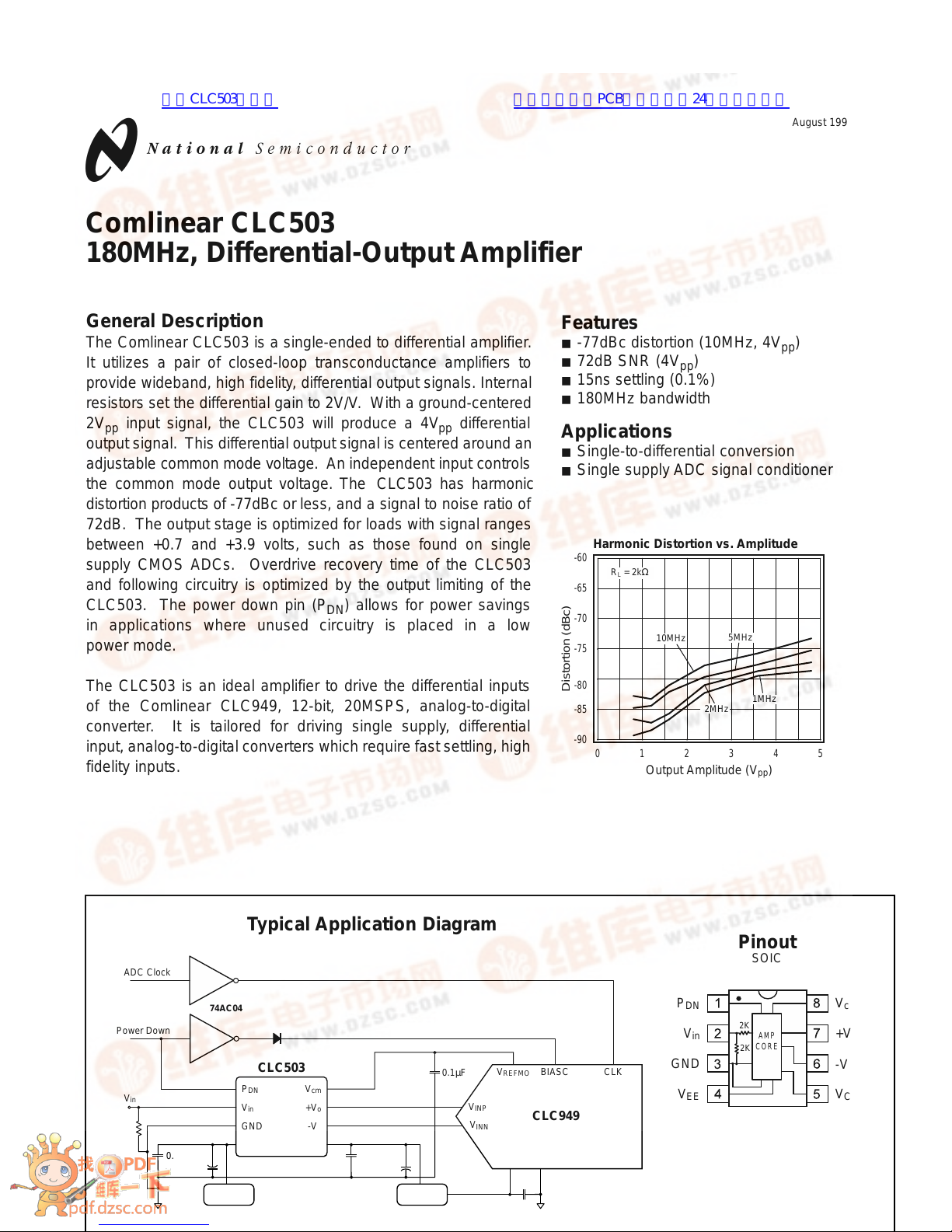
The Comlinear CLC503 is a single-ended to differential amplifier.
It utilizes a pair of closed-loop transconductance amplifiers to
provide wideband, high fidelity, differential output signals. Internal
resistors set the differential gain to 2V/V. With a ground-centered
2Vppinput signal, the CLC503 will produce a 4Vppdifferential
output signal. This differential output signal is centered around an
adjustable common mode voltage. An independent input controls
the common mode output voltage. The CLC503 has harmonic
distortion products of -77dBc or less, and a signal to noise ratio of
72dB. The output stage is optimized for loads with signal ranges
between +0.7 and +3.9 volts, such as those found on single
supply CMOS ADCs. Overdrive recovery time of the CLC503
and following circuitry is optimized by the output limiting of the
CLC503. The power down pin (PDN) allows for power savings
in applications where unused circuitry is placed in a low
power mode.
The CLC503 is an ideal amplifier to drive the differential inputs
of the Comlinear CLC949, 12-bit, 20MSPS, analog-to-digital
converter. It is tailored for driving single supply, differential
input, analog-to-digital converters which require fast settling, high
fidelity inputs.
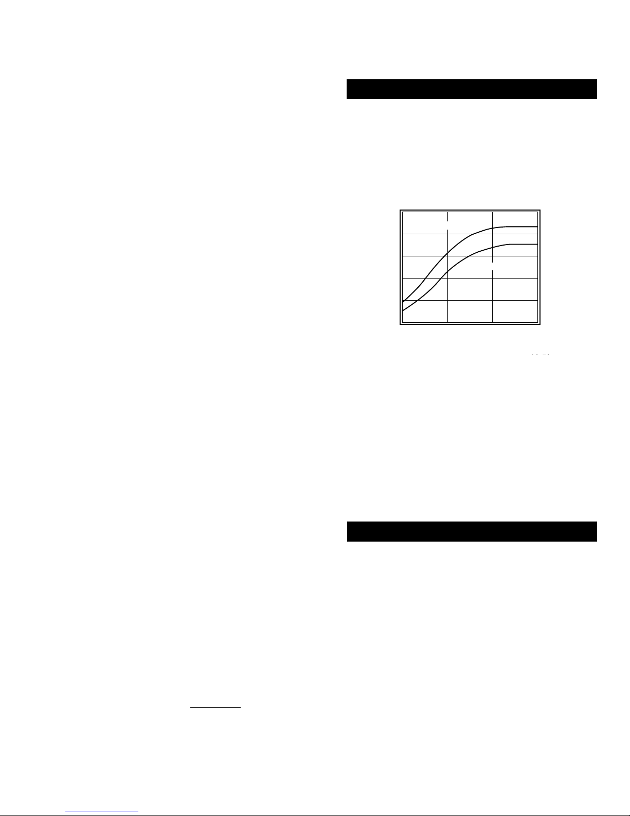
Harmonic Distortion vs. Amplitude
Distortion (dBc)
Output Amplitude (Vpp)
4123
5
R
L
= 2kΩ
-85
-80
-75
-70
-65
-60
10MHz
5MHz
2MHz
1MHz
-90
0
P
DN
V
in
GND
V
EE
+V
o
-V
o
V
CC
V
cm
2K
2K
AMP
CORE
Typical Application Diagram
Pinout
SOIC
V
in
P
DN
CLC503
CLC949
74AC04
Power Down
ADC Clock
V
in
GND
V
EE
V
cm
+V
o
-V
o
V
CC
V
REFMO
BIASC CLK
V
CC
GND
-5V
0.1µF
0.1µF
0.1µF
12b/20MSPS ADC
V
INP
V
INN
6.8µF
+5V
0.1µF
6.8µF
Comlinear CLC503
180MHz, Differential-Output Amplifier
August 1996
Comlinear CLC503
180MHz, Differential-Output Amplifier
N
查询CLC503供应商 捷多邦,专业PCB打样工厂,24小时加急出货
Page 2
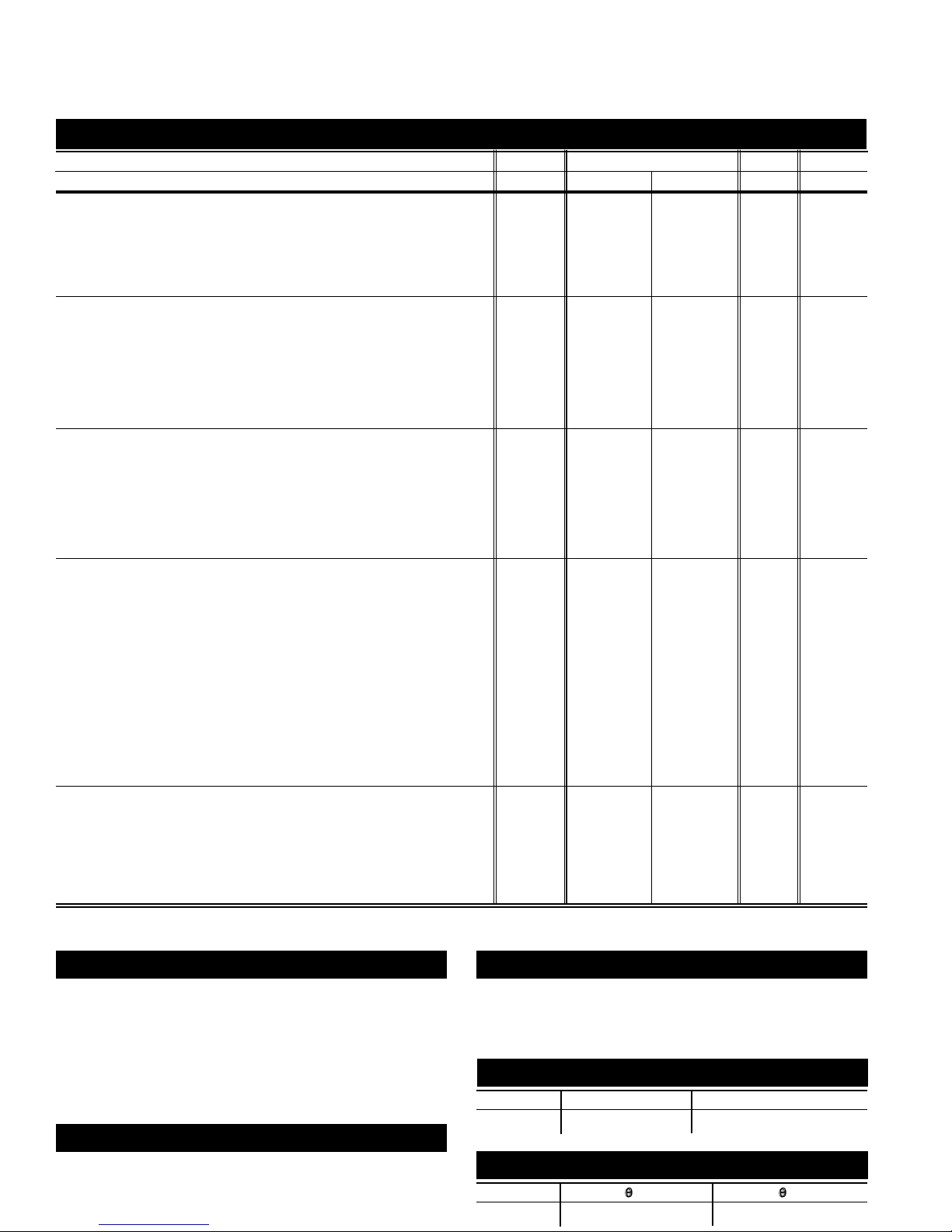
PARAMETERS CONDITIONS TYP MIN/MAX RATINGS UNITS NOTES
Ambient Temperature CLC503 +25˚C +25˚C -40 to 85˚C
FREQUENCY DOMAIN RESPONSE
Differential Amp
large signal bandwidth V
o
< 4.0V
pp
180 80 70 MHz
gain flatness DC to 10MHz 0.3 0.5 0.5 dB
Common-Mode Amp
-3dB bandwidth V
o
< 4.0V
pp
15 10 10 MHz
TIME DOMAIN RESPONSE
Differential Amp
rise and fall time 2V step 2.1 2.5 3.0 ns
settling time to 0.1% 2V step 15 22 25 ns
overshoot 2V step 0 %
slew rate 2V step 800 500 500 V/µs
Common-Mode Amp
recovery from power down 0.1% output settling 40 100 100 ns
DISTORTION AND NOISE RESPONSE
2
nd
harmonic distortion 4Vpp, 1MHz -78 -74 -70 dBc B
4V
pp
, 10MHz -75 -71 -71 dBc B
3
rd
harmonic distortion 4Vpp, 1MHz -85 -80 -79 dBc B
4V
pp
, 10MHz -77 -72 -72 dBc B
SNR 4V
pp
72 71 70 dB
integrated output noise voltage R
s
= 50Ω
10kHz – 500MHz 325 380 460 µV
rms
STATIC DC PERFORMANCE
Differential Amp
gain V
o
(Diff)/V
in
2 1.75 - 2.25 1.75 - 2.25 V/V A
output offset voltage V
in
= 0 10 90 100 mV A
INL 0.015 0.03 0.05 % A
R
in
2 1.6 - 2.4 1.6 - 2.4 kΩ
Common-Mode Amp
gain V
ocm/Vcm
0.97 0.9 - 1.1 0.9 - 1.1 V/V
output offset voltage 100 200 200 mV A
R
in
10 5 5 MΩ
input voltage range 1.5 - 3.5 V
power supply rejection ratio DC 50 30 30 dB A
supply current R
L
= ∞ 25 30 30 mA A
supply current, power down 4.5 6 6 mA A
MISCELLANEOUS PERFORMANCE
power down input CMOS levels 0.5 - 4.8 V C
V
IL
on 1 V
V
IH
off 4.5 V C
power down dissipation P
DN
= “Hi” 45 60 60 mW A
output voltage range single output 0.7 - 3.9 0.85 - 3.7 0.9 - 3.5 V
differential output resistance 500 400 - 600 375 - 625 Ω
Min/max ratings are based on product characterization and simulation. Individual parameters are tested as noted. Outgoing quality levels are
determined from tested parameters.
Electrical Characteristics
(VCC= + 5V, VEE= - 5V, Vcm= 2.25V, CL= 5pF, Vo= 4Vppunless specified)
Notes
A) J-level: spec is 100% tested at +25˚C, sample tested at +85˚C.
LC/MC-level: spec is 100% wafer probed at +25˚C.
B) J-level: spec is sample tested at +25˚C.
C) POWER DOWN must be 1V higher than Vcm.
Ordering Information
Model Temperature Range Description
CLC503AJE -40
˚
C to +85˚C 8-pin SOIC
Absolute Maximum Ratings
supply voltage
±
6V
maximum input range
±
6V
maximum output range (±V) 0 to V
CC
maximum operating temperature range -40˚C to +85˚C
maximum junction temperature +175˚C
maximum storage temperature range -65˚C to +150˚C
maximum lead temperature (soldering 10 sec) +300˚C
ESD rating (human body model) 500V
Recommended Operating Conditions
supply voltage
±
4.5 to ±5.5Vdc
input voltage ±1V
output voltage +0.8 to +3.75V
ambient temperature range -40°C to +85°C
Package Thermal Resistance
Package
q
JC
q
JA
SOIC (AJE) 65˚C/W 90˚C/W
Page 3
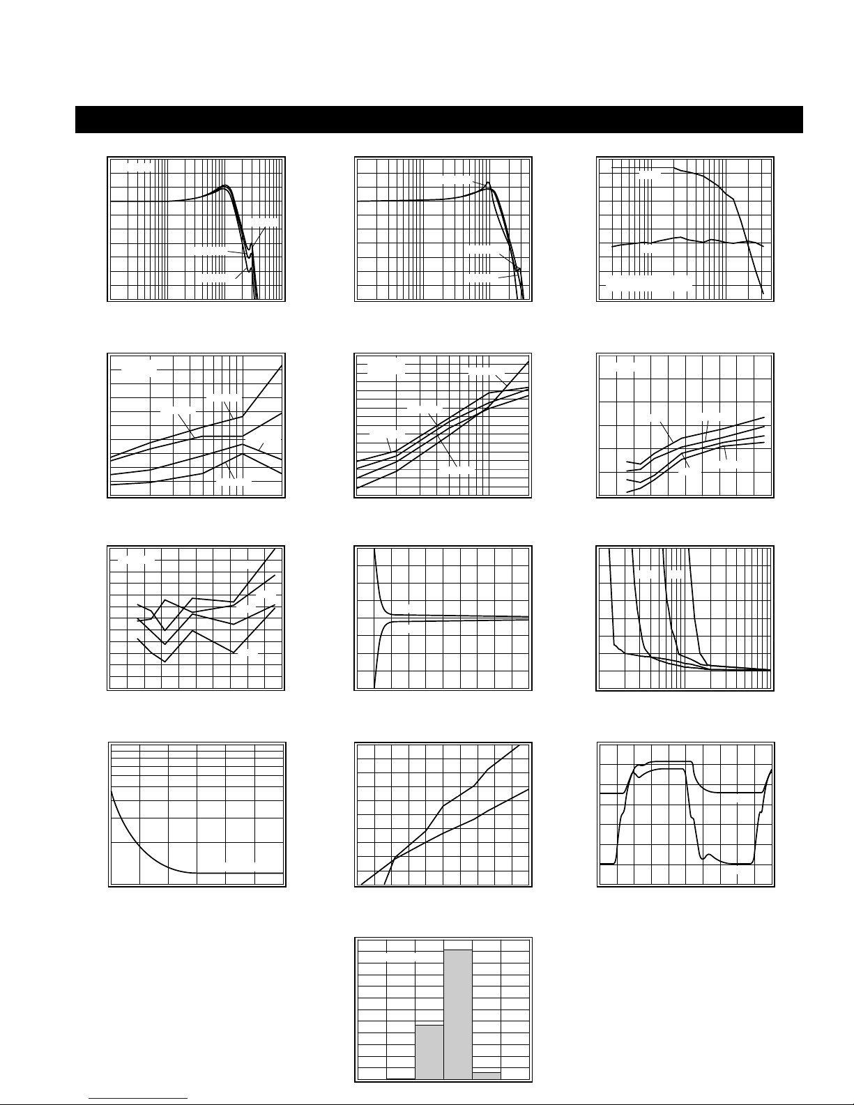
Typical Performance Characteristics
(VCC= + 5V , VEE= - 5V , Vcm= 2.25V , CL= 5pF, Vo= 4Vppunless specified)(
Frequency Response vs. R
L
Normalized Magnitude (1dB/div)
Frequency (Hz)
1M
10M
100M
RL = Open
RL = 500Ω
RL = 1kΩ
1G
Vo = 1V
pp
Frequency Response vs. V
o
Normalized Magnitude (1dB/div)
Frequency (Hz)
1M
10M
100M
Vo = 1V
pp
Vo = 3V
pp
Vo = 2V
pp
SNR and SFDR
SFDR (dBc), SNR (dB)
Frequency (Hz)
1M 10M
SFDR
SNR
55
60
65
70
75
80
CLC949 driven by CLC503
-1dB full scale input
2nd Harmonic Distortion vs. Frequency
Distortion (dBc)
Frequency (Hz)
0.1M
10M
Vcm = 2.75
-84
-82
-80
-78
-76
-74
Vcm = 2.25
Vcm = 1.75
Vcm = 1.25
Vin = 1.2V
pp
Vo = 2V
pp
3rd Harmonic Distortion vs. Frequency
Distortion (dBc)
Frequency (Hz)
0.1M
10M
Vcm = 2.75
-98
-96
-94
-92
-90
-88
-86
-84
-82
Vcm = 2.25
Vcm = 1.75
Vcm = 1.25
Vin = 1.2V
pp
Vo = 2V
pp
2nd Harmonic Distortion vs. Amplitude
Distortion (dBc)
Output Amplitude (Vpp)
4123
5
R
L
= 2kΩ
-85
-80
-75
-70
-65
-60
10MHz
5MHz
2MHz
1MHz
-90
0
3rd Harmonic Distortion vs. Amplitude
Distortion (dBc)
Output Amplitude (Vpp)
1234
5
R
L
= 2kΩ
-90
-85
-80
-75
-70
10MHz
5MHz
2MHz
1MHz
-95
-100
0
Pulse Response CLC949 Driven By CLC503
Error (%)
Time (ns)
0 20406080100
Positive
Negative
-1.0
-0.5
0
0.5
1.0
Settling Time vs. Capacitive Load
Error (%)
Time (ns)
10 100 1000
5pf
-0.1
0
0.1
0.2
0.3
0.4
0.5
0.6
0.7
10pf 20pf
40pf
Equivalent Input Noise
Voltage Noise (nV/√Hz)
Frequency (Hz)
0.1k
1M
100M
Voltage = 12nV/√Hz
10
100
10M100k1k 10k
IB, VIO, vs. Temperature
V
IO
(mV)
Temperature (°C)
-100 -50 0 50 100 150
I
B
(µA)
2.155
I
B
-30
2.16
-25
2.165
-20
2.17
-15
2.175
-10
2.18
-5
V
IO
Power Down (PDN) Response
Amplitude (1V/div)
Time (20ns/div)
P
DN
Output
0
-1
-2
1
2
3
4
5
CLC949 Output When Driven By CLC503
Code Occurances
3000
2500
500
2012 2013 2014 2015 2016 2017
2000
1500
0
Input Grounded
1000
Page 4
CLC503 APPLICATIONS
APPLICATION CONSIDERATIONS
Theory of Operation
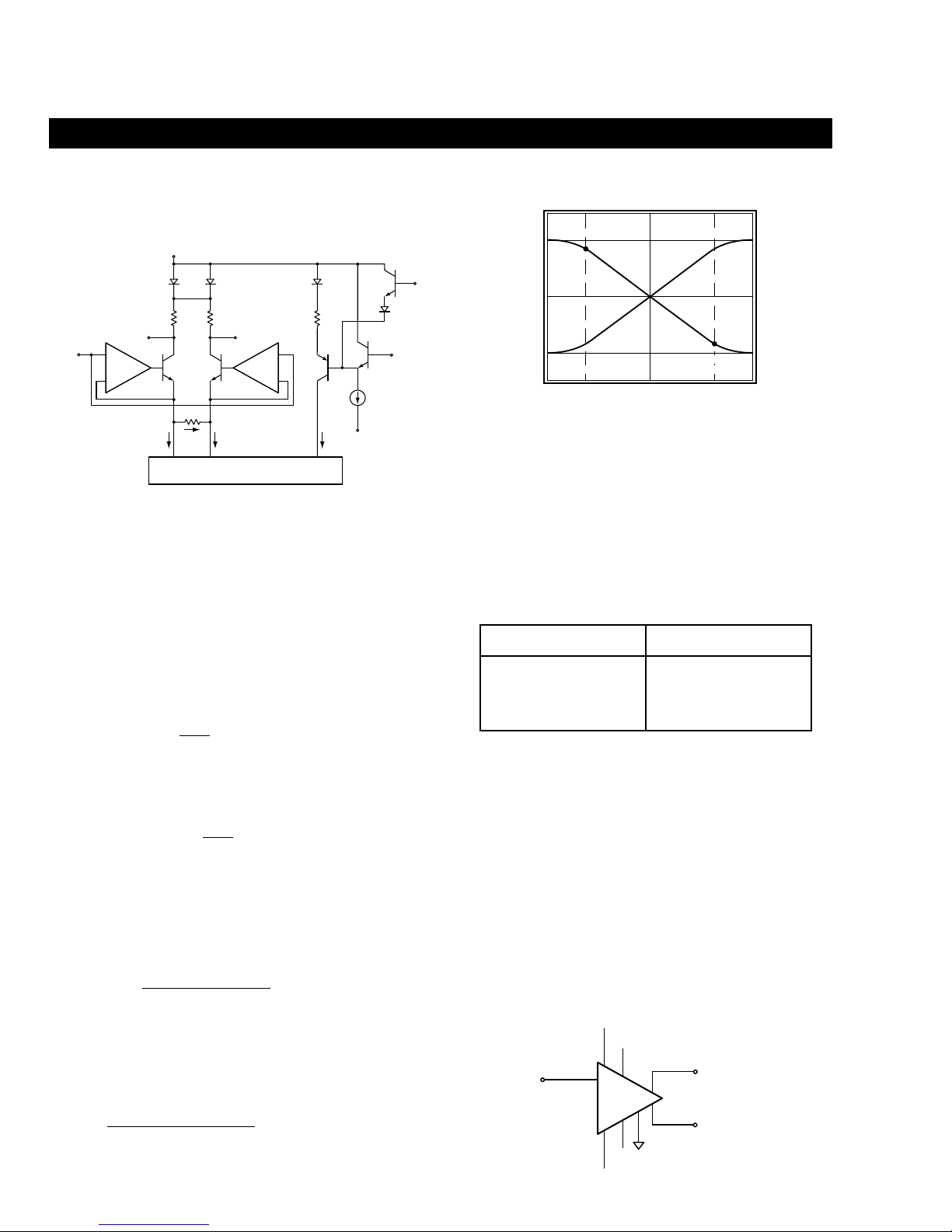
Figure 1 is a simplified schematic of the CLC503.
Figure 1: Simplified Block Diagram
The input voltage drives a unity gain buffer, B1, and
an inverting buffer, B2. These buffers drive emitter
followers, Q1and Q2. Resistor, R3, is the gain set
resistor. The combination of B1, B2, Q1, Q2and R
3
form a transconductance stage. The input voltage
across R3is converted to an in-phase and out-ofphase current through the collectors of Q1and Q2. The
current through R3is:
The common mode voltage across R4is converted
to a current. Transistor Q5has a collector current
equal to:
The common mode current is scaled and mirrored back
to Q1and Q2. These currents, I, are converted back to
a voltage at the collector load resistors, R1and R2.
This forms the common-mode output voltage.
V
ocm
= VCC– V
diode
– R1I
I = 16I
cm
V
ocm
= V
cm
Figure 2 depicts the differential output voltage limits of
the CLC503.
Figure 2: Differential Output Voltage
Centered around Vcm, the outputs are derived from the
following equations.
The input to output relationship is shown in Figure 3.
V
in
V
odiff
±1V ±2V
2V
pp
4V
pp
±1.4V max ±2.8V max
Figure 3: Input vs. Output Relationship
Pulling the power down line (PDN) high decreases the
quiescent supply current. This turns off the current
flowing in Q5, and therefore Q1and Q2, allowing the
output voltages to drift high, to approximately 4.3V.
Since the signal is not significantly attenuated, P
DN
does not effectively isolate the input from the output.
This part is not recommended for use as a multiplexer.
Refer to
Pin Descriptions - Power Down pin
section. No damage occurs to the device when PDNis
high and the input is driven to the supply voltage.
Pin Descriptions
Figure 4: CLC503 Functional Pin Descriptions
+1
-V
o
+V
in
B1
Q
1
R
1
V
CC
R
3
I
-1
+V
o
B2
Q
2
R
2
I
R
4
I
cm
Q
5
Q
4
Q
4
V
EE
P
DN
V
cm
I
3
Current Mirror
R1 = R2
2 R1 = R3 R4 = 16R1
Output Voltage (V)
Input Voltage (V)
3.7
0.8
-1
0
1
2.25
3.25V
1.25V
V
cm
+Vo = V
cm +Vin
-Vo = V
cm -Vin
+V
o
V
in
P
DN
2
3
1
7
V
CC
5
-V
o
6
V
cm
8
V
EE
4
I
2V
R
VIRIRRR
VI2R
V
2V
R
2R 2R R
V2V
3
in
3
odiff
31 32 1 2
odiff
31
odiff
in
3
113
odiff
in
=
=+ =
=
()
=
()
=
=
I
VVV
R
R 16R
cm
CC
cm
diode
4
41
≈
−−
=
+V V V
-V V V
V+V-V2V
ocm
in
ocm
in
odiff
oo
in
=+
=−
==–( )
IV V V
R
CC
cm
diode
1
=−−
Page 5
■
Pin 1
Power Down (PDN): The power down pin takes
CMOS input levels. Use this to decrease the
power from 250mW to 40mW. This is not a
signal disable pin. A CMOS gate will drive this
input. The quiescent supply current will be
decreased when PDNis at least 1V higher than
Vcm. When the current is turned off, the output
voltage Vo, will go to approximately 4.3V. An
internal pull down resistor of 10k allows PDNto
be left open when not used.
■
Pin 2
Input V oltage (Vin): This is the signal input. The
recommended input range is ±1V. The linear
operating range is approximately ±1.4V This
input controls the differential output voltage.
Because of the closed loop nature of the transconductance stage, the transfer function is highly
linear. Refer to
Output Voltage
pin for output
signal limitations.
■
Pin 3
Ground (GND): Tie to low impedance analog
ground.
■
Pins 4 and 5
Power Supplies (VEEand VCC): For optimum
performance, use linear ±5V power supplies.
Use bypass capacitors of 0.1µF and 6.8µF on the
power supply lines to decrease any noise that
could be injected into the circuit by the power
supplies. Place the bypass capacitors as close
to the device pins as possible. Remove the
ground plane from the board underneath the
device to eliminate parasitic capacitance. Refer
to
Printed Circuit Board Layout
section for
more layout suggestions.
■
Pins 6 and 7
Output Voltage (-Voand +Vo): These are the
differential signal output pins. The output voltage
at these pins is limited to 0.7V to 3.9V. The
output recovery time after exceeding these limits
is approximately 40ns. The output voltage can
be defined as:
■
Pin 8
Common-Mode Voltage (Vcm): This input sets
the common-mode output operating points. The
common mode input voltage can range from 1.5V
to 3.5V. Refer to
Output Voltage
pin discussion
for limitations on the output range.
Load: The CLC503 is intended to drive high speed
CMOS analog-to-digital converters, such as the
CLC949. Resistive loading will affect the gain and
common mode offset. It is not recommended to drive
resistive loads below 10kΩ with this part. See Figure 5
for gain vs. load with specified range in device output
resistance.
Figure 5: Gain vs. Resistive Load
Settling Time: The CLC503 settles to 0.1% in 15ns
with a 5pF load, the input capacitance of the CLC949.
Refer to the
Settling Time vs. Capacitive Load
plot in
the
Typical Performance Characteristics
section.
Power Dissipation
To calculate the power dissipation, PT, for the CLC503,
use the following equation:
The performance of the CLC503 is strongly dependent
on proper layout, and adequate power supply
decoupling. The parasitic capacitance at the output of
the CLC503 and the input to the CLC949, or any other
analog-to-digital converter, must be kept to a minimum.
Consider the following guidelines:
■
Use a ground plane.
■
Bypass power supply pins with monolithic
capacitors of 0.1µF and with 6.8µF tantalum
capacitors. Place the capacitors less than 0.1"
(3mm) from the pin.
■
Remove the ground plane underneath the
device and 0.1" (3mm) from all input/output
pads.
Interfacing the CLC503 with the CLC949
The CLC503 can be easily interfaced with the CLC949
as shown in Figure 6. An evaluation board is available
for proto-typing and measurements.
PI V V
T
CC CC
EE
=−
()
+V V V
-V V V
V+V-V2V
V
+V -V
2
V
ocm
in
ocm
in
odiff
oo
in
ocm
oo
cm
=+
=−
=− =
=
−
=
()
()
Gain (V/V)
Load Resistance (Ω)
2
1.5
0
100
1000
10000
1
0.5
100000
2.5
Ro = 600Ω = R
omax
Ro = 400Ω = R
omin
Design Information
Printed Circuit Board Layout
Page 6
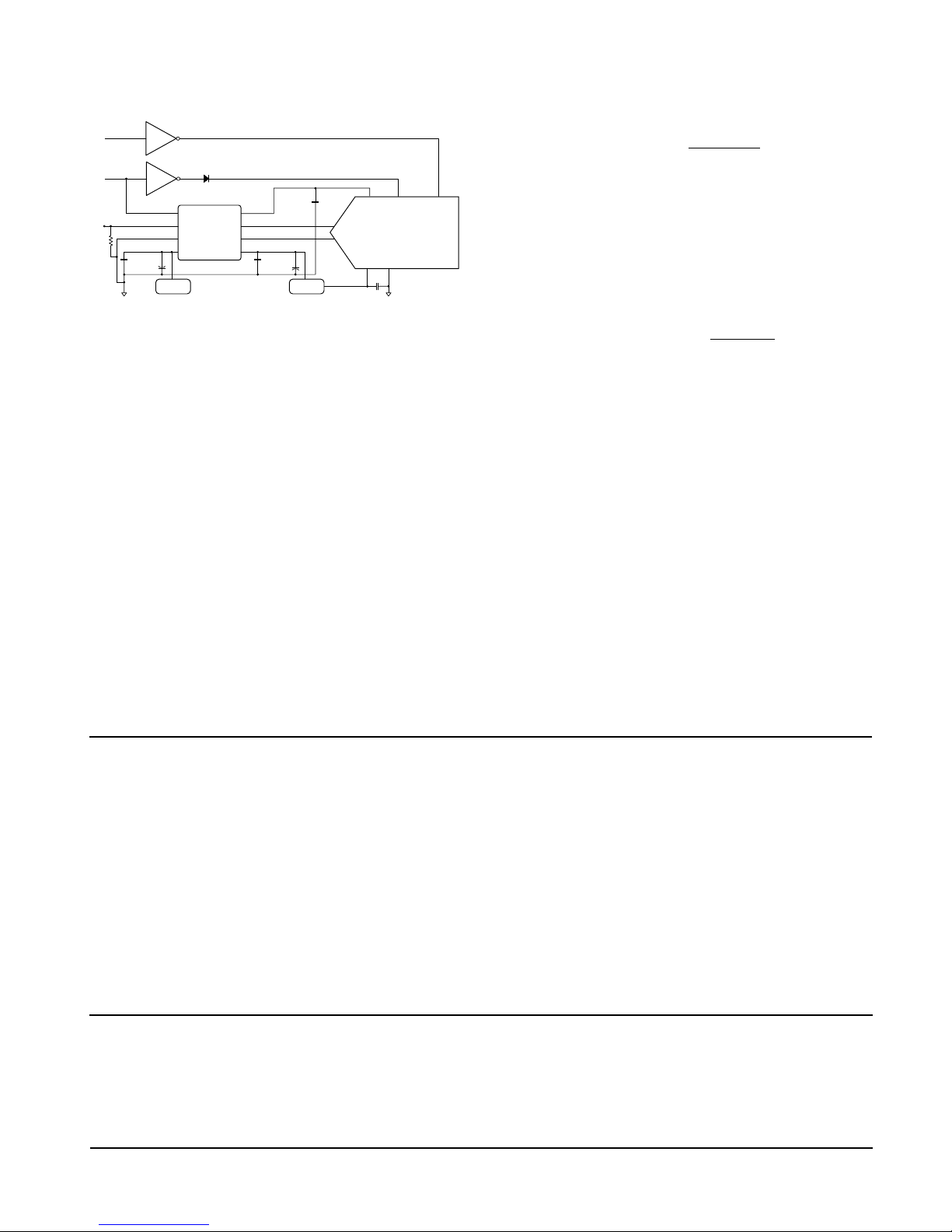
Figure 6: Interfacing the CLC503 with the CLC949
Extended Use Considerations
Designed to drive the CLC949, the CLC503 can be
used with other analog-to-digital converters. The user
will want to consider the following parameters of the
device that the CLC503 will drive.
■
Input impedance of the A/D. Refer to Figure 5
for the Gain vs. Resistive Load. The CLC503
operates best when driving resistive loads
greater than 10kΩ and capacitive loads of less
than 10pF.
■
Resistive loading will affect the gain and common
mode offset. The gain setting resistors are
fixed internally. The voltage gain equation is:
where RLequals the input resistance of the A/D. The
impact of lower values of RLis shown in Figure 5. The
tolerance on the 500Ω is ±20%.
■
Capacitive loading will affect the settling time.
The settling time equation is:
where Rs= 250Ω ±15% and %settling ≥ 0.1%. Refer
to the
Settling Time vs. Capacitive Load
plot in the
Typical Performance Characteristics
section.
■
Other considerations
■
Output signal swing must be within the
specified output range.
■
Common mode range must meet the
specified common mode range.
■
Distortion will be affected when Vinand
Vcmdrive the output out of the linear
operating range.
Comlinear CLC503
180MHz, Differential-Output Amplifier
AA
500 ||R
500
vv
L
new
old
=
Ω
Ω
t RCln
100%
%settling
settle
s
L
=⋅⋅
V
in
P
DN
CLC503
CLC949
74AC04
Power Down
ADC Clock
V
in
GND
V
EE
V
cm
+V
o
-V
o
V
CC
V
REFMO
BIASC CLK
V
CC
GND
-5V
0.1µF
0.1µF
0.1µF
12b/20MSPS ADC
V
INP
V
INN
6.8µF
+5V
0.1µF
6.8µF
Customer Design Applications Support
National Semiconductor is committed to design excellence. For sales, literature and technical support, call the
National Semiconductor Customer Response Group at 1-800-272-9959 or fax 1-800-737-7018.
Life Support Policy
National’s products are not authorized for use as critical components in life support devices or systems without the express written approval
of the president of National Semiconductor Corporation. As used herein:
1. Life support devices or systems are devices or systems which, a) are intended for surgical implant into the body, or b) support or
sustain life, and whose failure to perform, when properly used in accordance with instructions for use provided in the labeling, can
be reasonably expected to result in a significant injury to the user.
2. Acritical component is any component of a life support device or system whose failure to perform can be reasonably expected to
cause the failure of the life support device or system, or to affect its safety or effectiveness.
National Semiconductor National Semiconductor National Semiconductor National Semiconductor
Corporation Europe Hong Kong Ltd. Japan Ltd.
1111 West Bardin Road Fax: (+49) 0-180-530 85 86 13th Floor, Straight Block Tel: 81-043-299-2309
Arlington, TX 76017 E-mail: europe.support.nsc.com Ocean Centre, 5 Canton Road Fax: 81-043-299-2408
Tel: 1(800) 272-9959 Deutsch Tel: (+49) 0-180-530 85 85 Tsimshatsui, Kowloon
Fax: 1(800) 737-7018 English Tel: (+49) 0-180-532 78 32 Hong Kong
Francais Tel: (+49) 0-180-532 93 58 Tel: (852) 2737-1600
Italiano Tel: (+49) 0-180-534 16 80 Fax: (852) 2736-9960
National does not assume any responsibility for use of any circuitry described, no circuit patent licenses are implied and National reserves the right at any time without notice to change said
circuitry and specifications.
N
 Loading...