

COMCHIP TV15C5V0K-B, TV15C5V0J-B, TV15C6V0K-B, TV15C6V0J-B, TV15C6V5K-B User Manual
...
查询TV15C100J供应商
SMD Transient Voltage SuppressorSMD Transient Voltage Suppressor
TV15C5V0 Thru TV15C171
Working Peak Reverse Voltage: 5.0 - 170 Volts
Power Dissipation: 1500 Watts
Features
Ideal for surface mount applications
Easy pick and place
Plastic package has Underwriters Lab.
flammability classification 94V-0
Typical IR less than 1uA above 10V
Fast reponse time: typically less 1nS for
uni-direction, less than 5nS for bi-
directiona, from 0 V to BV min.
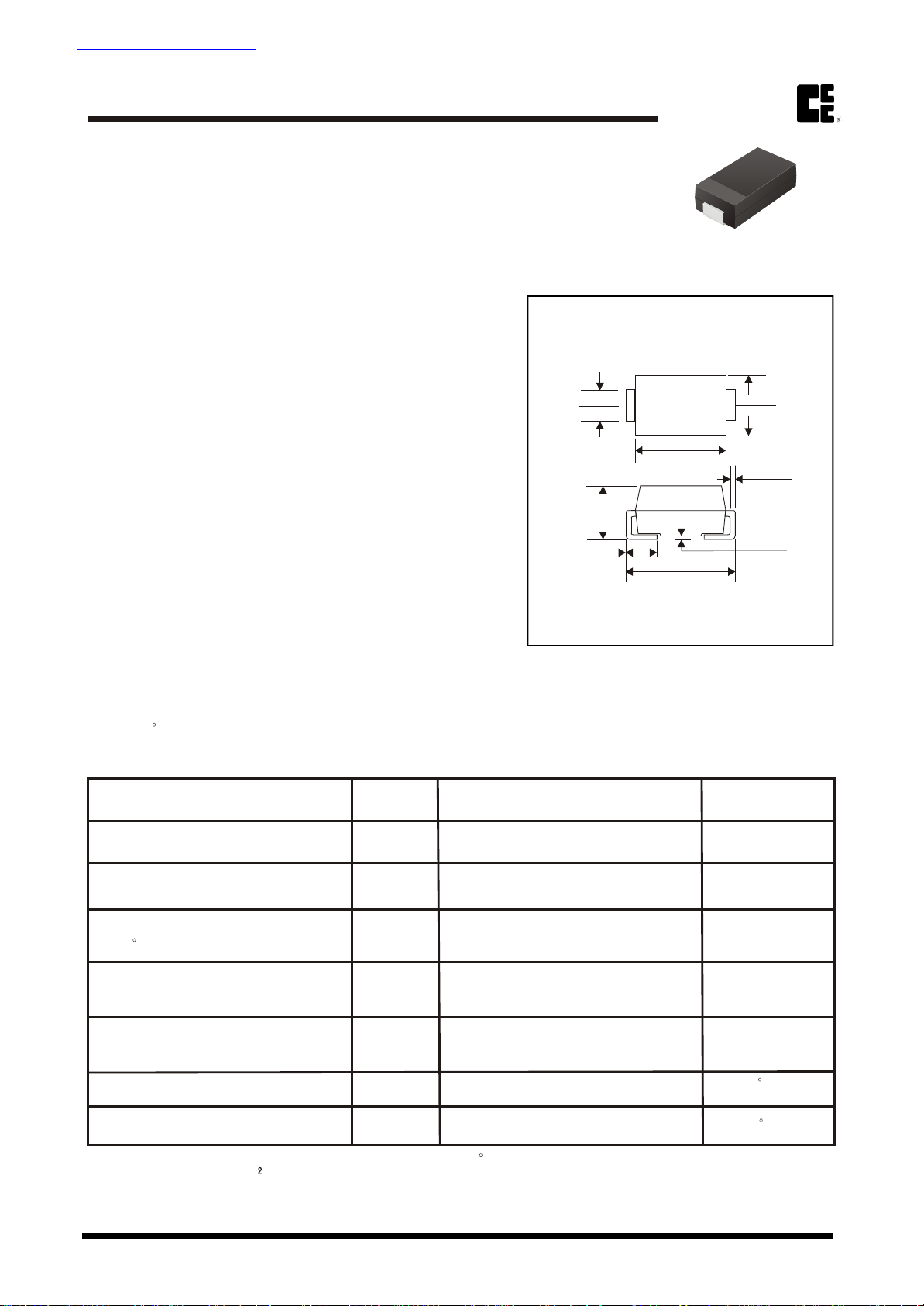
Mechanical data
Case: JEDEC DO-214AB molded plastic
Terminals: solderable per MIL-STD-750,
method 2026
Polarity: Cathode band denoted
Mounting position: Any
Approx. Weight:0.21 gram
0.124(3.15)
0.108(2.75)
0.050(1.27)
0.030(0.76)
COMCHIPCOMCHIP
www.comchip.com.tw
SMC/DO-214AB
0.280(7.11)
0.260(6.60)
0.103(2.62)
0.079(2.00)
Dimensions in inches and (millimeter)
0.320(8.13)
0.305(7.75)
0.245(6.22)
0.220(5.59)
0.012(0.31)
0.006(0.15)
0.008(0.20)
0.0203(0.10)
Maximum Ratings and Electrical Characterics
Rating at 25 C ambient temperature unless otherwise specified.
Single phase, half wave, 60Hz, resistive or inductive load.
For capacitive load, derate current by 20%
Characteristics
Peak Power Dissipation on 10/1000uS
Waveform (Note 1, Fig. 1)
Peak Pulse Current of on 10/1000uS
Waveform (Note 1, Fig. 3)
Steady State Power Dissipation at
TL=75 C (Note 2)
Peak Forfard Surge Current, 8.3mS Single
Half Sine-Wave Superimposed on Rated
Load, Uni-Directional Only (Note 3)
Maxinum Instantaneous Forward Voltage
at 100A for Uni-Directional only
(Note 3 & 4)
Operation Junction Temperature Range
Storage Temperature Range
Note: 1. Non-Repetitive Current Pulse, per Fig. 3 and Derated above TA=25 C, per Fig. 2.
2. Mounted on 8.0x8.0 mm . Copper Pads to Each Terminal.
3. Measured on 8.3 mS Single Half Sine-Wave or Equivalent Square Wave, Duty Cycle=4 Pulse per Minute Maximum.
4. VF=3.5V on TV15C5V0 thru TV15C900 Devices and VF=5.0V on TV15C101 thru TV15C171.
Symbol
PPPM
IPPM
PM(AV)
IFSM
VF
Tj
TSTG
Value
1500
See Table 1
5.0
200
3.5/5.0
-55 to +150
-55 to +150
Units
Watts
A
Watts
A
Volts
C
C
MDS0211016A
Page 1
SMD Transient Voltage SuppressorSMD Transient Voltage Suppressor
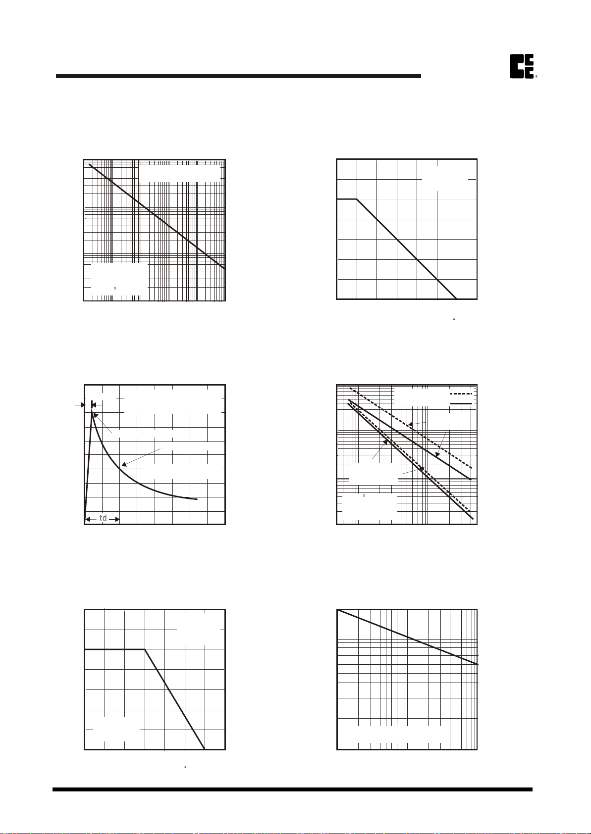
Rating and Characteristic Curves (TV15C5V0 Thru TV15C171)
COMCHIPCOMCHIP
www.comchip.com.tw
Fig. 1 - Reverse Characteristics
100
10
1.0
Non-Repetitive
Peak Pulse Power, PPPM (KW)
Pulse Waveform
Shown in Fig. 3
TA=25 C
0.1
0.1 1.0 10 100 1000 10000
Mounted on 8mmx8mm
Copper Pads
Pulse Width, td (uS)
Fig. 3 - Pulse Waveform
125
tr =10uS
100
75
50
25
Peak Pulse Current, IPPM ( %)
0
0 1.0 2.0 3.0 4.0
Pulse Width (td) is Defined
as the Point Where the peak
Current Decay to 50% of Ipp
Peak Value IPPM
Half Value Ipp/2
10/1000 uS Waveform
as Defined by R.E.A.
Time, t (mS)
Fig. 2 - Pulse Derating Curve
140
Mounted on
120
100
80
60
40
20
Peak pulse Power (Ppp) or Current (Ipp)
Derating in Percent (%)
0
0 25 50 75 100 125 150 175
Ambient Temperature,TA ( C)Ambient Temperature,TA ( C)
5mmx5mm
Copper pads
Fig. 4 - Typical Junction Capacitance
for Uni-Directional Devices
10,000
Uni-Directional
Bi-Directional
1,000
Measure at
100
Junction Capacitance, Cj (pF)
0
Standard-off
Voltage, Vwm
Tj=25 C
f=1.0MHz
Vsig=50mVp-p
5.0 10 100 500
Breakdown Voltage,VBR (Volts)
Measure at
Zero Bias
Fig. 5 - Steady State Power Derating Curve
7.0
6.0
5.0
4.0
3.0
2.0
Steady State Power Dissipation,
PM(AV), Watts
1.0
0
MDS0211016A
Mounted on
8mmx8mm
Copper pads
0 25 50 75 100 125 150 175
Leadt Temperature,TL ( C)
60Hz
Resistive or
Inductive
Load
Fig. 6 - Maxinum Non-Repetitive Peak
Forward Surge Current (Uni Directional Only)
200
100
50
20
Peak Forward Surge Current, IFSM (A)
8.3mS Single Half Sine-Wave
(JEDEC Method) Tj=Tjmax
10
1 10 100
Number of Cycle at 60Hz
Page 2
 Loading...