

Page 1

主板型号
C.NC65 Ver1.4A
Colorful C.NC65 Ver1.4A
品 质
务
服
:
艺 术
说明书版本 1.0
七彩虹网站 http://tec.colorful.cn
http://seethru.colorful.cn
http://info.colorful.cn
服务论坛 http://bbs.colorful.cn/bbs
七彩虹信箱 support@seethru.com.cn
800 免费服务热线 800-830-5866
I
Page 2

Colorful C.NC65 Ver1.4A
版 权
本手册版权属于世和资讯公司所有,未经本公司书面许可,任何人不
得对此说明书和其中所包含的任何资料进行复制、拷贝或翻译成其它
语言。
声 明
因 IT 市场变化迅速,编辑时间有限,本手册仅供用户参考使用,不保
证没有任何错误,不提供任何形式的担保。本公司保留对手册内容修
订和更改的权力。对于所作修改,公司没有责任通知任何个人。
商标版权
本手册中有使用到其他公司的注册商标,特声明如下:
Microsoft 、MS-DOS 和 Windows 是微软公司(Microsoft Corp.)的
注册商标。
AMD、Athlon™、Duron™是 AMD 公司的注册商标。
其他在本说明书中使用的产品名称是他们各自所属公司所拥有和被公
认的。
世和资讯公司对本手册拥有最终解释权。
II
Page 3

Colorful C.NC65 Ver1.4A 目录
使 用 手 册 目 录
主机板简介
主机板规格
处理器……………………………………...……………………………...
芯片组…………………………………………...………………………...
内存…………………………………………………...……………….…..
板载 IDE………………………………………………………….
AGP 介面 ………………………………………………..……………….
扩展插槽 ………………………………………………………..…………
数据线
安全性能
串行 ATA………………………………………………………..…………
存储
内建 8 声道 Codec 控制器…………………….……………………….
BIOS………………………………………………………………...…….
…………………………………………...………………………...
…………………………………………………...……………….…..
………………………………………………………….….
………………………………………………………….….
…….…..
………………………………………………………..…………
1
2
2
2
2
2
3
3
3
3
3
3
4
4
超级 I/O 功能 ………………………………………………………….….
电源管理 ……………………………………….……………………….
主板结构 ……………………………………….……………..………..
Colorful C.NC65 Ver1.4A主机板缩略图 ………………….…………
硬体设定
主板布局图 .....………………………..………………….……………..
Colorful C.NC65 Ver1.4A主机板架构索引 ………………………….
跳线设置 …………………………………..…….…………………….….
……………………………………….……………..………..
III
4
4
4
5
5
5
6
7
Page 4

Colorful C.NC65 Ver1.4A 目录
连接口介绍....…………………………………………….………..…....
..…...........…………………...........………………..
硬件安装步骤
驱动程序安装
BIOS 设定
Award BIOS 设定主菜单
标准 CMOS 设定
高级 BIOS 设定
高级芯片设定 ..…
外部设备选项
电源管理设定
PNP/PCI 即插即用 …...........…………………...........………………..
系统即时状态
载入优化预设值
管理者使用者密码
…
..…...........…………………...........………………..
..…
..…...........…………………...........………………..
..…
...........…………………...........…………..
..…...........…………………...........………………..
..…...........…………………...........………………..
..…...........…………………...........………………..
..…...........…………………...........………………..
..…
..…...........…………………...........………………..
..…
..…...........…………………...........………………..
..…
..…...........…………………...........………………..
…
.…...........…………………...........………………..
8
14
18
20
2
2
2
2
3
3
4
4
4
4
1
3
5
9
3
8
1
3
8
8
离开 SETUP 并储存设定结果
离开 SETUP 但不储存设定结果..…...........………
NVIDIA RAID的组建
在 Windows 下管理 NVIDIA RAID
六声道音效设置
...........…………………...........………………..
..…...........…………………...........………………..
…
开机系统自检常见错误讯息
BIOS的更新方法
...........…………………...........………………..
主板专有名词缩写对照
客户技术支持
..…...........…………………...........………………..
…
....…………………...........…………..
…
.............………...........…………..
..…...........………...........…………..
..…...........………...........…………..
...
....
IV
...........…………..
9
4
0
5
0
5
5
6
6
1
6
7
9
6
1
7
3
7
Page 5

Colorful C.NC65 Ver1.4A
C.NC65 Ver1.4A 主机板简介
——感受 AMD 龙族的激进性能 切入性能价格的黄金分割点
感谢您购买七彩虹 C.NC65 Ver1.4A 主板。C.NC65 Ver1.4A 主板采用 M-ATX架
构,支持 AMD Socket AM2 的 AMD Athlon 64 FX/Athlon 64/Sempron CPU,支
持 HyperTransport 1GHz,支持 DDR2 533/DDR2 667/DDR2 800 标准内存。
芯片组采用 Nvidia MCP61V,支 持 1.8V DDR SDRAM,提 供 4 根 240-pin DIMM
插槽,最高可支持 4GB 的双通道 DDR 2 800 规格内存。支持 PCIE x1 接口,提
供 1 个 IDE 接口、2 个 SATA2 接口(支持 RAID0、1 和 JBOD)和 8 个 USB 接
口(其中 4 个需要用 CABLE 连出)。
C.NC65 Ver1.4A 支持 2 个 PCI 插槽、1 个 PCI x16 槽(支持 x1 的传输速度)和 1
个 PCI x1 槽,可供加插各种高性能的扩展卡。
主板包装合内附标准组件
一块 C.NC65 Ver1.4A 主板
一条 SATA 数据线和电源转接线
一条软盘驱动器带状电缆
一条 IDE 驱动器带状电缆
一本 C.NC65 Ver1.4A 主板中文用户手册
一张驱动光盘
一张质量保证卡
1
Page 6

Colorful C.NC65 Ver1.4A
机 板 规 格
主
主要特性
处理器
支持 AMD Socket AM2 CPU
支持 AMD Athlon™ 64 X2 Dual-Core 处理器
支持 AMD Athlon™ 64 FX 处理器
支持 AMD Athlon™ 64 处理器
支持 AMD Sempron™ 处理器
支持 AMD Cool’n’Quiet 技术
芯片组
nVIDIA nForce MCP61V
AMD Athlon 64 CPU支持 Hyper Transport 技术
支持系统和电源管理
支持 2 IDE 磁盘驱动器, 2 个 SATA2 磁盘驱动器,完整的 RAID 0、RAID 1、
JBOD 功能
支持 PIO 模式 5, Bride Mode 和 Ultra DMA 33/66/100/133 总线控制模
支持 8 个 USB 2.0 接口
符合 PCI Version 2.3 规范
符合 AC’97 Version 2.3 规范 SATA 2.0 规范
符合 SATA 2.0规范
Fast A T A/133 IDE 控制
内存
提供 4 条 240-pin 1.8V 内存插槽
支持双通道 DDR2 533/DDR2 667/DDR2 800 SDRAM
最大内存容量支持至 4 GB
板载 IDE
支持 2 个 IDE 磁盘驱动器
支持 PIO 模式 4, 块模式和 Ultra DMA 33/66/100/133 总线控制模式
2
Page 7

Colorful C.NC65 Ver1.4A
PCI-Express
提供一个 PCI-E 16X 插槽, 支持每秒 250MB 单向带宽
可支持部分 x16 的显卡,支持 x1 传输速度
扩展插槽
提供一个 PCI-E x1 插槽,2 条 PCI 插槽,兼容 PCI2.2
网卡
板载 Realtek RTL8100C
支持 10 Mb/s, 100 Mb/s 自动转换
半双工/全双工
支持 ACPI 电源管理
串行 ATA
支持 2 个串行 ATA (SATA) 端口
符合 SATA 2.0 规范
数据传输速度达到 3GB/s
存储
NVIDIA RAID 技术
RAID 0 加快高级系统的运行速度
RAID 1 支持磁盘镜像数据备份功能
JBOD将不同的磁盘驱动器合并成一个逻辑驱动器
支持 SATA 和 ATA-133S 磁盘控制器标准
内建显示核心
集成 Geforce 6100 显示核心,基於 NV44 的绘图核心
支援 Direct X 9.0、Shader Model 3.0 等,並拥有 2 个 Pixel Shader 流水线
及 1 个 Vertex Shader 流水线,
Geforce 6100 标准频率为 475MHz
3
Page 8

Colorful C.NC65 Ver1.4A
音频控制器
板载 8 声道 HD AUDIO
支持 16bit 立体声解码
支持多路立体声混频
提供前置音频接口,麦克风接口
BIOS
使用 Award BIOS 的 4Mb Flash EEPROM
支持进阶电源组态管理程序(ACPI)
支持 SMBIOS (系统管理 BIOS) v2.2 兼容
支持电源故障恢复
超级 I/O 功能
提供超级 I/O 控制芯片
芯片: Winbond W83627HG-AM
1 个 IDE 接口可连接 2 个 IDE 设备
2 个 SATA2 接口(支持 RAID0,1, JBOD)
1 个 FDD 接口
1 个 EPP/ECP/SPP 并行接口
8 个 USB2.0 接口(4 个内建 USB 需用 Cable 导出使用),理论可支持
480MB/s 的传输数率。
电源管理
支持 ACPI 1.0B 和 APM 1.2 规范
支持定时开机
主板结构
MATX 构架
尺寸: 20.4 cm x 24.5cm ( 宽 x 长)
4
Page 9
Colorful C.NC65 Ver1.4A
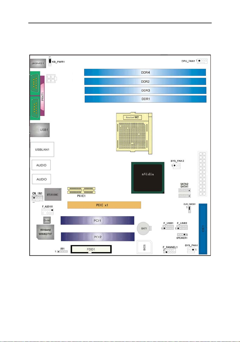
硬 件 设 定
C.NC65 Ver1.4A 主机板布局图
◇此主板有一个标准的电源接口和一个单独的 12V 电源接口,
只可使用标准的 ATX 12V 电源。
◇请将连接线的红色端连接到连接头标记“1”脚的那一端。
◇ 建议不要在 CPU 座背面加金属片,以免造成短路。
标明第一个针脚.
(
)
5
Page 10
Colorful C.NC65 Ver1.4A
C.NC65 Ver1.4A 主机板架构索引
6
Page 11
Colorful C.NC65 Ver1.4A
A
B
C
D
E
F
G
H
I
J
KB_PWR1: 键盘鼠标唤醒
后置面板接口
F_AUDIO1:前置音频接头
PCIE x1 插槽(加速图形卡接口)
CD_IN1: CD-ROM 音频输入接头
IR1:红外设备接头
FDD1: 软驱接口
F_USB1~2: USB 前置接头
SYS_FAN1: 系统风扇接头
SPEAK、F_PANEL1:前置面板接口
K
O
P
Q
R
S
T
U
V
IDE1: 硬盘接口
CLR_CMOS: 清除 CMOS 跳线
SATA1~2: 串行 ATA 连接器
ATX 24 PIN 接口
SYS_FAN2: 系统风扇接头
DDR1~4: DDR DIMM 模组
CPU_FAN 接头
ATX12V 电源接口
PCIE x1 接口
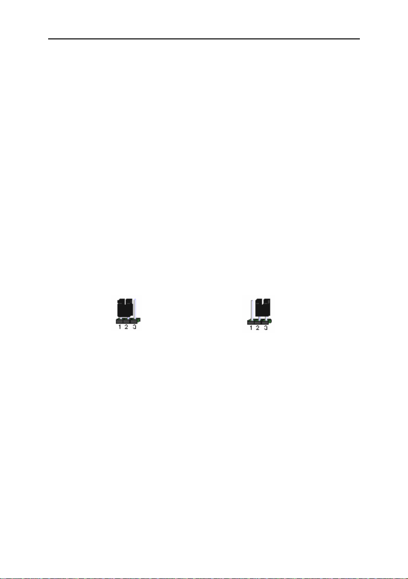
跳线设置
CLR_CMOS–BIOS 清除跳线
CLR_CMOS 是个 3 脚的插针,如果忘记了系统密码,可以用此来清
除掉。
1—2:正常模式 b. 2—3:清除 CMOS
a.
清除 CMOS 的步骤:
关闭电脑并且拔下电源线。
从“POWER”插槽上拔出 ATX 电源连接线。
把 CLR_CMOS 上的跳帽跳到 2-3 短路,并等几秒钟。
将 CLR_CMOS 上的跳帽重新回 1-2 短路。
插回 ATX 电源线,并插上交流电源。
7
Page 12
Colorful C.NC65 Ver1.4A
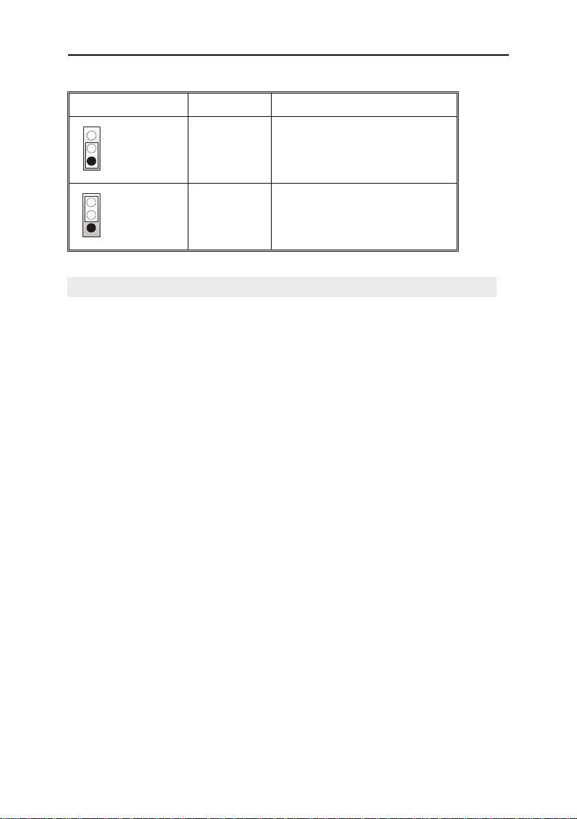
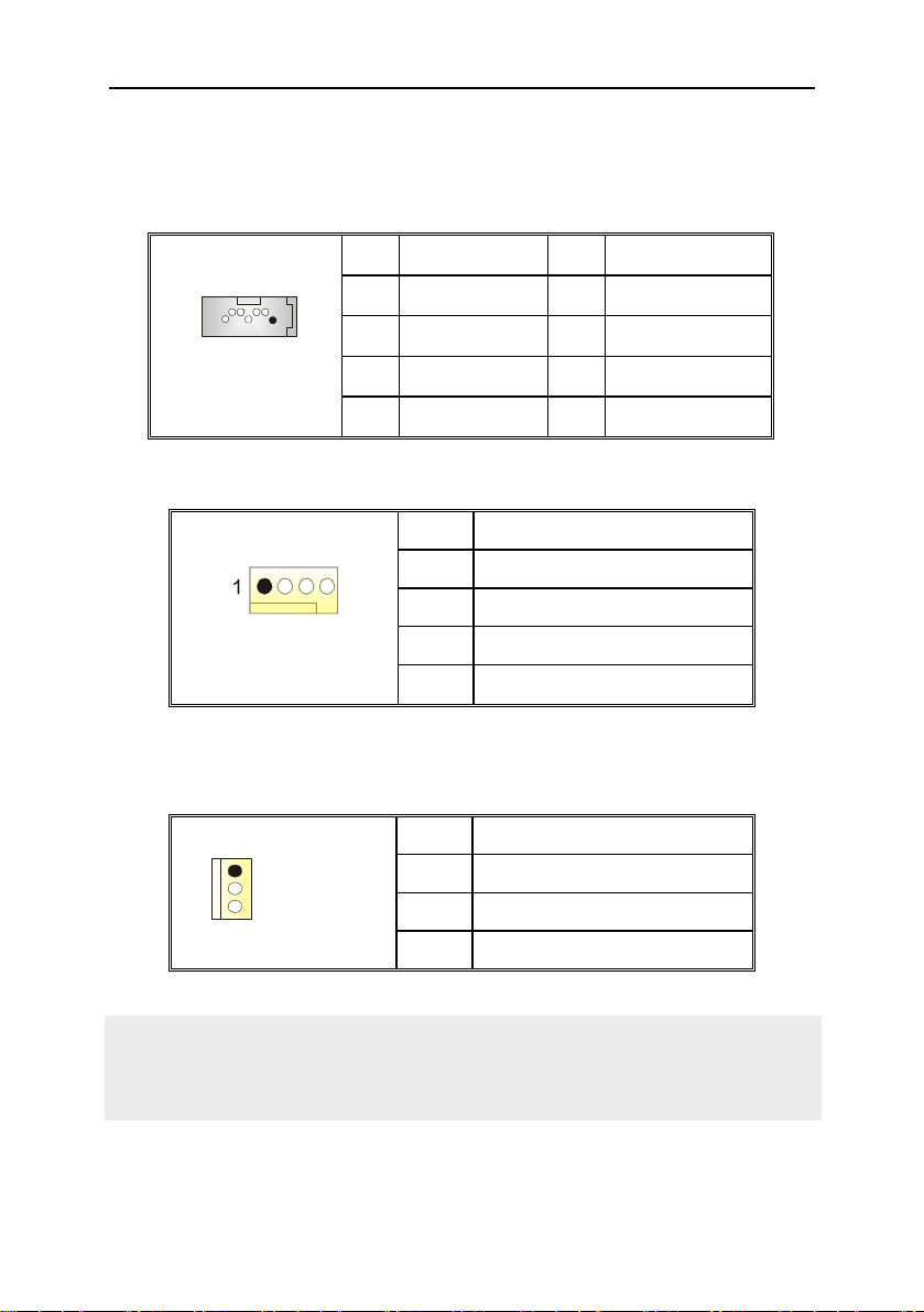
盘开机跳线选择: KB_PWR1
KB_PWR1
3
1
Pin 1-2 闭合
3
1
Pin 2-3 闭合
+5V 关闭键盘开机功能
+5V 唤醒
定义 描述
使用+5V 唤醒电压,开启键盘开
机功能
注意:
要开启键盘开机功能, “KB_PWR1”跳线应该放置在 Pin 2-3 上。
连接口介绍
软驱(FDD)连接口 FD1
软驱连接口是 34 针的接口,支持 360K, 720K, 1.2M, 1.44M 和 2.88M
类型的软盘用于连接软驱。
硬盘接口: IDE1
此款主板有一个 32 位增强型的 PCI IDE 控制器,可提供 PIO 模式 0~5,
总线控制模式和 Ultra DMA 33/66/100/133 功能.一个硬盘接口: 可接
主从模式 IDE 设备。
IDE接口可以联接主\从硬盘驱动器,所以你可以同时联接达2个硬盘驱
动器。
外部设备插槽: PCI1~2
此主板配有 2个标准的 PCI插槽,PCI既是外部互联设备,也是一个扩展
卡总线标准.PCI 插槽为 32 位。
8
Page 13
Colorful C.NC65 Ver1.4A
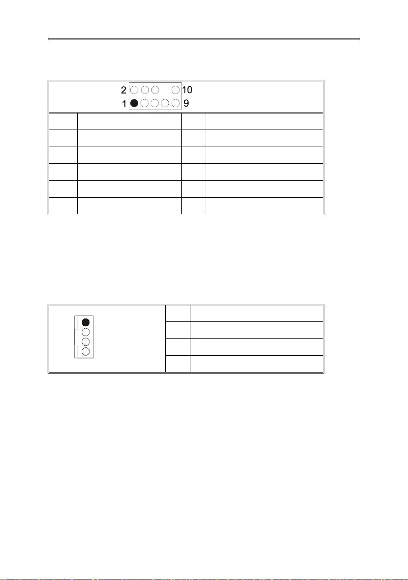
串行 ATA 接口: SATA1~2
主板有一个在双通道 SATA接口的 nForce MCP61 的 SATA控制器.其符
合 SATA 2.0 规范.传输速度为 3Gb/s。
7
SATA1~4
针脚
定义
1
接地
1
TX-
3
5 RX- 6 RX+
7
接地
针脚 定义
2 TX+
4
接地
CPU 风扇接头: CPU_FAN1
CPU_FAN1
系统风扇接头: SYS_FAN1~2
针脚 定义
1
2 +12V
3
4
接地
风扇 RPM 检测
风扇控制信号
1
SYS_FAN1
注意:
CPU_FAN1 和 SYS_FAN1 都支持采用智能监控的冷却风扇系统,其连
接接口是 3 针头.当连接线嵌入连接器内,请注意红线是正极,须接到第
二个针脚,黑线接地须接到 GND 针脚。
针脚 定义
1
2 +12V
3
接地
风扇 RPM 检测
9
Page 14
Colorful C.NC65 Ver1.4A
IR 红外设备接头:IR1
针脚 定义
1 VCC
IR1
2 NC
3 RX
4 GND
5 TX
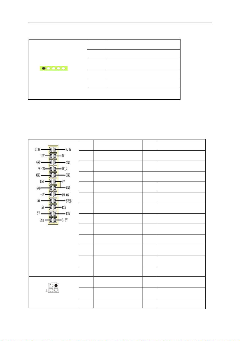
电源接口: PWRATX1/ATX 12V1
PWRATX1:此连接器允许用户连接 ATX 电源供应的 24针脚电源接口。
ATX 12V1:连接此连接器将提供 12V 电压给 CPU 电路。
针脚 定义 针脚 定义
接地
1
2
+3.3V
13
接地
14 +5V
PWRATX1
1
2
3
ATX 12V1
3 +5V 15
4 +12V 16
5 +5V 17 PS_ON
6 +12V 18 TP_2
7 +5V 19
唤醒 +5V
8
9 -5V 21 +12V
10 PW-OK 22 +5V
11
接地
12
接地
针脚 定义 针脚 定义
1 +12Vz 3
2 +12v
10
20
23
24
4
接地
接地
接地
接地
+3.3V
+3.3V
接地
接地
Page 15
Colorful C.NC65 Ver1.4A
右
左
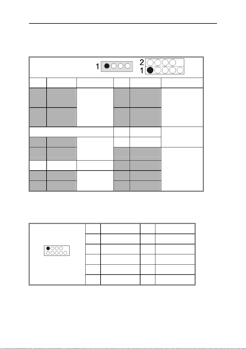
前置音频接口: F_AUDIO1
用户将连接器连接 PC 前置音频输出时,此时后置面板音频同样输出.
F_AUDIO1
针脚 定义
1 Mic-IN 2 MIC GND
针脚
定义
3
Mic-BIAS
5
声道输出
7 GND 8 NC
9
声道输出
4 NC
6
后置右声道输出(可不接)
10
后置左声道输出(可不接)
CD-ROM 音频输入接头: CD_IN1
此连接器允许用户连接多种设备以取声源,如 CD-ROM, DVD-ROM,
PCI 声卡, PCI TV 调谐卡等。
1
JCDIN1
针脚
1
2
3
定义
左声道输入
接地
接地
11
Page 16
Colorful C.NC65 Ver1.4A
前置面板接口: F_PANEL1
此 13 针脚连接器包含开机, 重启, 硬盘指示灯, 电源指示灯, 休眠按
钮, 扬声器. PC 前置面板含开关功能。
Speak、F_PANEL1
针脚 定义 功能 针脚 定义 功能
HDD LED
1
(+)
硬盘指示灯
3 HDD LED
(-)
2 Power LED
(+)
电源指示灯
4 Power LED
(-)
6
电源按钮
8
接地
11 N/A
5
接地
7
重启控制
开机按钮
重启按钮
10
+5V
12 N/A
13
扬声器
扬声器连接口
前置 USB 接头: F_USB1~2
1
2
F_USB1/F_USB2
10
针脚
1
3 USB- 4 USB5 USB+ 6 USB+
7
9 Key 10
定义
+5V (保险)
接地
针脚
2
8
定义
+5V (保险)
接地
NC
PC 前置面板有附加 USB 数据线,可像 USB 读卡器连接 USB 设备。
12
Page 17
Colorful C.NC65 Ver1.4A
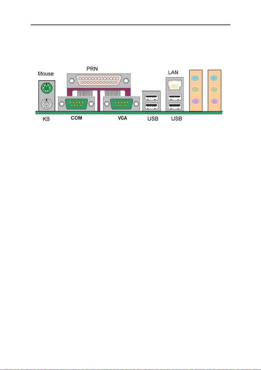
后面板接口
键盘/鼠标、USB、串 口 COM2 并口 LPT1、RJ45 网络接口、MIC_IN、
LINE_IN、LINE OUT 都接在后面板上,详细情况见下图:
键盘/鼠标
接口形式为 PS/2,上面印有“KEYBOARD”和“MOUSE”字样。
USB(通用串行接口)
通用串行接口上印有“USB”字样,主板上后面板有 2 对 USB 接口,
可用于接 USB 器件,另有两组为插针形式 F_USB1/2。
VGA(视频输出接口)
板载显卡输出接口。
COM(串行输出接口)
可连接串行设备。
LAN(RJ45)
板载 10/100 Mbps 自适应网卡。
外接音效接口(可选)
ALC650 为 3 个接口,ALC850 为 6 个接口。连接方法可参照附录。
线路输出(line-out),线路输入(line-in),麦克风输入(mic-in)。
重低音输出、后置环绕输出、环绕音效输出
13
Page 18

Colorful C.NC65 Ver1.4A
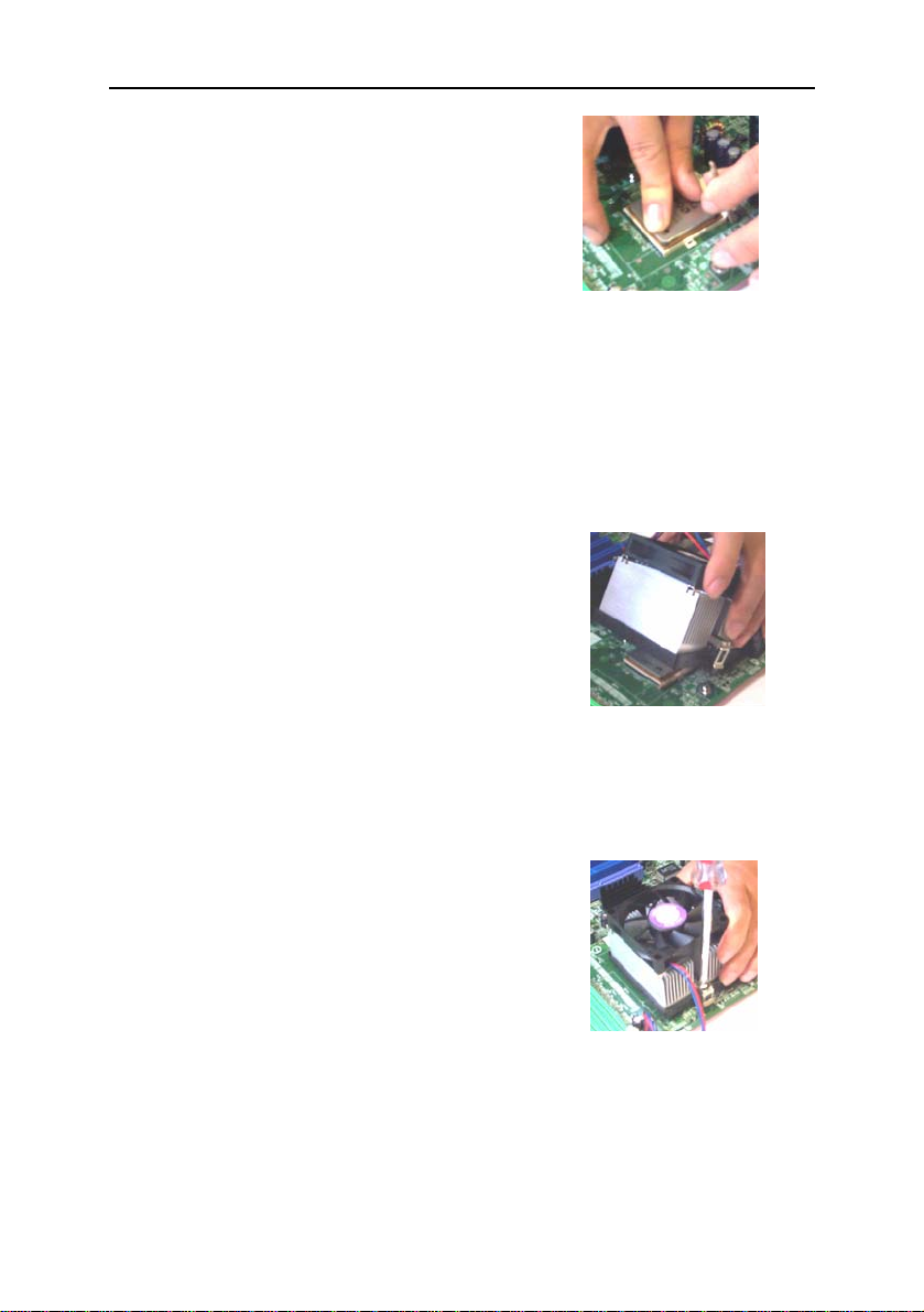
硬件安装步骤
请依据下列方式,完成电脑的安装:
1. 安装中央处理器(CPU)
2. 安装内存
3. 装入机箱
4. 安装所有扩展卡
5. 连接所有讯号线、排线、电源线及面板控制线
安装 CPU
主板内建有开关式电压调节器(Switching Voltage Regulator),支持
CPU Vcore 自动检测。即本主板能检测及辨识 CPU 电压、时钟、倍
频。用户通过 BIOS 设定屏幕中“Advanced Chipset Features(高级芯
片设定)”可查看 CPU 频率。
警告:
1. CPU 的散热器和风扇必须是经过 AMD 所认可的。
2. 板上安装散热器和风扇时,主板必须放在一个牢固的地方,以避
免晃动。
3. 散热器必须紧紧地安装到 CPU 上端。
4. 散热器没有正确和牢固地安装,请不要运行处理器。否则可导致
永久损害。
以下步骤显示如何安装 CPU、风扇和散热装置。首先, 找到主板上的
CPU 插槽。
将锁杆向上抬起 90 度
14
Page 19
Colorful C.NC65 Ver1.4A
1. 安装 CPU, 将插座拐角标记对准锁
杆顶部最近的插座拐角, 确定管角 1 的
方向正确。不要用力插 CPU,确信 CPU
完全插入插槽中。
在 CPU 上面涂上一层散热物质, 如散
热膏或硅脂,然后安装经过 CPU 制造
商认可的带散热片的风扇, 以避免损害
CPU。详情请参照 CPU 制造商网站。
向下按住控制杆以固定 CPU 幷锁在
旁边的卡槽中。
将带散热片的风扇放在 CPU
上面, 然后向下按两个塑料夹以钩
住支撑块两侧的孔。
2. 向下按每个塑料夹的白色扳杆,
将风扇套件固定在支撑块上。
15
Page 20
Colorful C.NC65 Ver1.4A
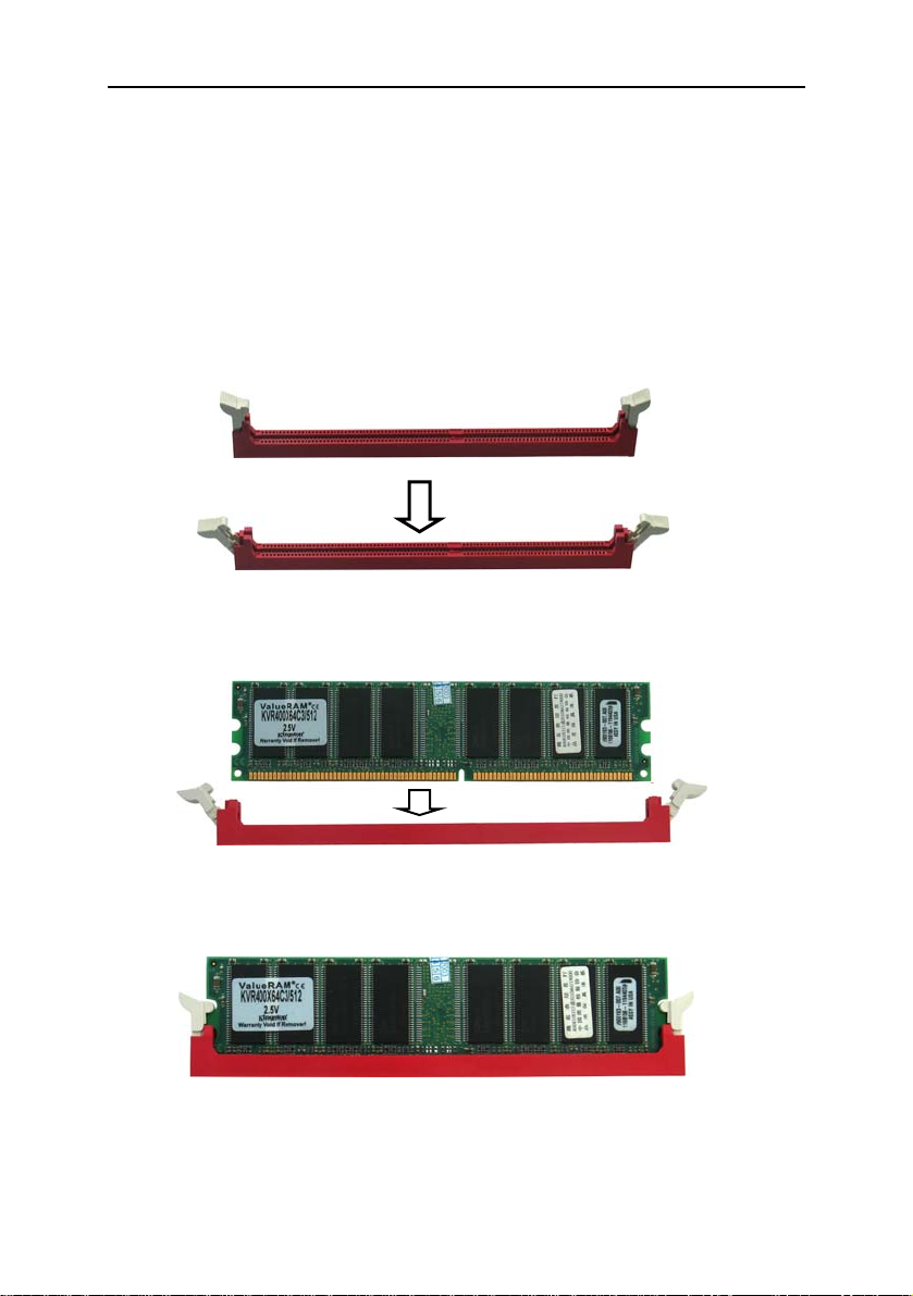
■安装内存
主板上有提供 4 条 240-pin 1.8V 插槽,支持双通道 DDR2 533/DD R2
667/DDR2 800 SDRAM,最大内存容量可支持至 4 GB。
内存速度可以经由BIOS来控制,您可以在“Advanced Chipset
Features Setup”页找到若干个关于SDRAM速度的项目。详细细节请
参考BIOS章节。
安装内存步骤如下:
a.将内存条插槽两端的白色固定卡扳开;
b.将内存条的金手指对齐内存条插槽,并且在方向上要注意金手
指的两处凹孔要对上插槽的两处凸起点;
c.将内存条插入插槽中,插槽两端的白色卡子会因为内存条置入
而自动扣到内存条两侧的凹孔中。
16
Page 21

Colorful C.NC65 Ver1.4A
■安装主板到机箱
您很容易地将它安装到机箱上,请把随机箱提供的铜柱套入正确孔位,
并锁上螺丝以固定主机板,以防止主机板与机箱之间造成短路而损坏
主机板。
■安装所有扩展卡
您可以很容易的将你所需要的 PCIE 或 PCI 扩展卡安装到主机板上,
并锁上螺丝以固定扩展卡,以免造成扩展卡与主板之间的接触问题。
■连接所有讯号线、排线、电源线及面板控制线
具体细节请参考连接头介绍
温馨提示:
装卸主板及其它电脑元件时,请遵循以下基本预防措施:
a.配戴合适的静电手环并确定手环自然接地。
b.碰触一接地或防静电表面或一金属固定物如水管等。
c.避免接触扩展卡、主板及通过其接口插在扩展槽中的模组上的零
件。最好通过其装载托架处理系统元件。
以上方法可防止静电产生及正确释放静电。
17
Page 22
Colorful C.NC65 Ver1.4A
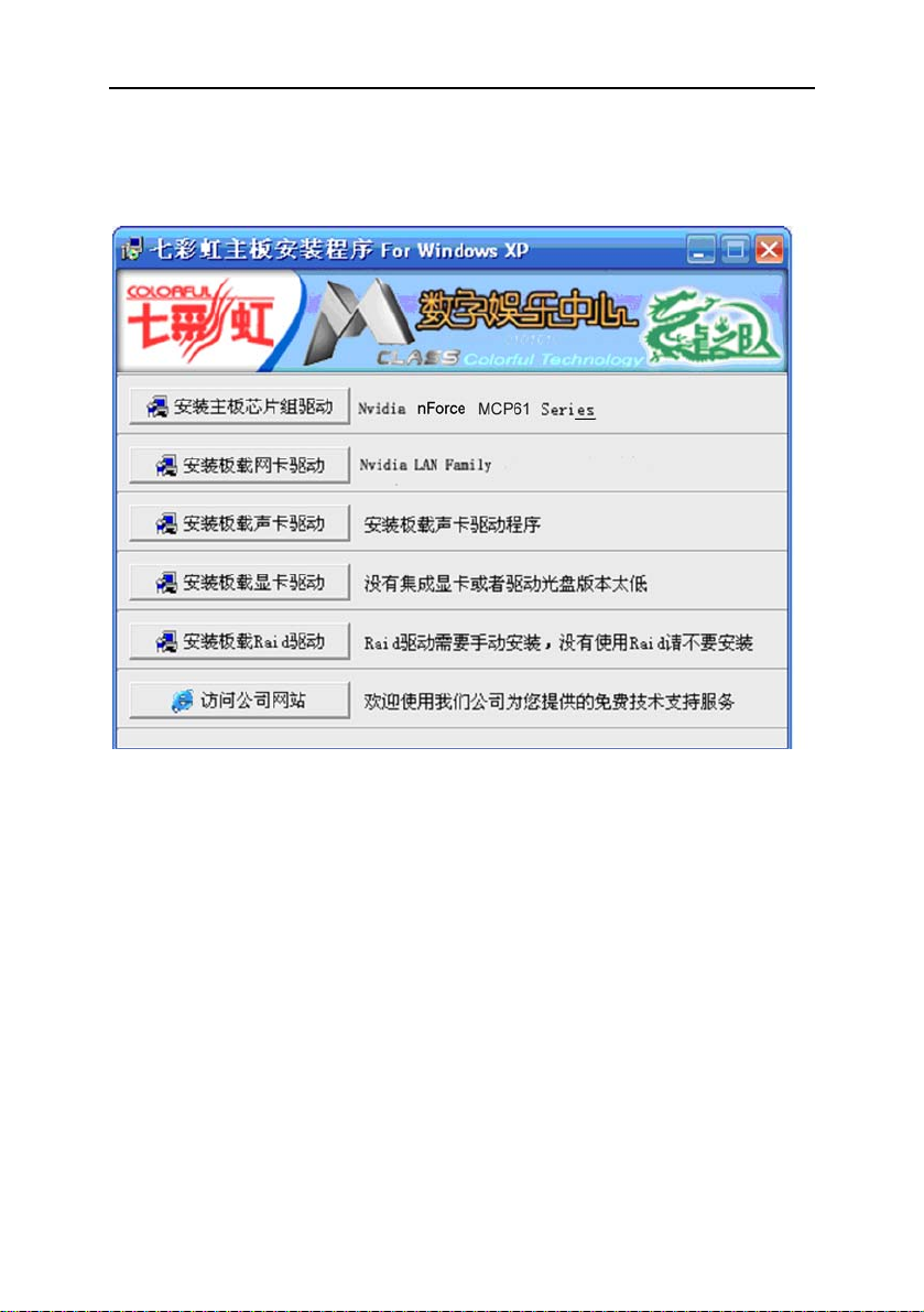
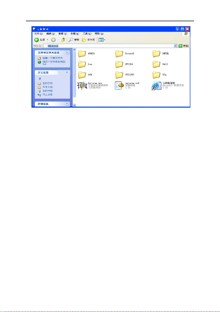
驱动程序安装说明
插入七彩虹主板驱动程序安装光盘,安装程序自动运行,弹出下面窗
驱动光盘能自动检测主板所使用的芯片组型号、声卡型号、板载显卡
型号或者板载网卡型号,点击相应的按钮安装相应的驱动。
您可以点击菜单上的按扭直接安装有关驱动。关于 USB2.0 驱动,如
果您使用 Win98 系统,请由附送驱动光盘安装;如果您使用 Win2000
系统,只需打上 SP4 的补丁;如果您使用 WinXP 系统,只需打上 SP1
的补丁。
口
18
Page 23
Colorful C.NC65 Ver1.4A
如果以上窗口中没有您的主板型号或所需驱动,可以在系统设备管理
器中指定光盘相关目录搜索安装,或者单击光驱盘符,右击打开光盘
文件,进入相应目录,安装所需驱动程序。
以下是一些主要设备驱动的光盘路径:
主板芯片组 INF 驱动:X:\Nvidia\setup.exe
注意:由于芯片组厂商的驱动程序不断更新以提高性能及解决兼容性
问题,我们的驱动盘中尽量采用目前较新的驱动版本,今后用户驱动
程序升级可关注我们网站中的更新,恕不另行通知。
19
Page 24

Colorful C.NC65 Ver1.4A
BIOS 设定
!!!注意:由于主板的 BIOS 版本在不断的升级,所以,本手册中
有关 BIOS 的描述仅供参考。我们不保证本说明书中的相关内
容与您所获得的信息的一致性。
CMOS SETUP 会将设置好的各项数据储存在主板上内建的
CMOS SRAM 中。当电源关闭时,由主板上的锂电池继续为 CMOS
SRAM 供电。BIOS 设置实用程序允许你配置:
◇硬盘驱动器,软盘驱动器,和周边设备
◇视频显示类型和显示选项
◇密码保护
◇电源管理特征
◇其它
进入 CMOS SETUP 设置
电源开启后,当 BIOS 开始进行 POST(Power On Self Test 开机自检)
时,按下<Del>键便可进入 AwardBIOS 的 CMOS SETUP 主画面中。
如果您来不及在 POST 过程中按<Del>键进入 CMOS SETUP,您可
以补按<Ctrl>+<Alt>+<Del>热启动或按机箱上的 Reset 按钮,以重新
开机再次进 POST 程序,再按下<Del>键进入 CMOS SETUP 程序中。
功能键说明
Ç(向上键) 移到上一个项目
È(向下键) 移到下一个项目
Å(向左键) 移到左边的项目
Æ(向右键) 移到右边的项目
Esc 键 退出当前画面
Page Up 键 改变设定状态,或增加栏位中的数值内容
Page Down
键
改变设定状态,或减少栏位中的数值内容
F1 功能键 显示目前设定项目的相关说明
F5 功能键 装载上一次设定的值
F6 功能键 装载最安全的值
F7 功能键 装载最优化的值
F10 功能键 储存设定值并离开 CMOS SETUP 程序
20
Page 25

Colorful C.NC65 Ver1.4A
主画面的辅助说明
当您在 SETUP 主画面时,随着选项的移动,下面显示相应选项的主
要设定内容。
设定画面的辅助说明
当您在设定各个栏位的内容时,只要按下<F1>,便可得到该栏位的设
定预设值及所有可以的设定值,如 BIOS 缺省值或 CMOS SETUP 缺
省值。如果想离开辅助说明窗口,只须按<Esc>键即可。
Award BIOS 设定主菜单
当您进入 CMOS SETUP 设定菜单时,便可看到如下的主菜单,在主菜单
中您可以选择不同的设定选项,按上下左右方向键来选择,按<Enter>
键进入子菜单。
Standard CMOS Features
Advanced BIOS Features Load Fail-Safe Defaults
Advanced Chipset Features Load Optimized Defaults
Integrated Peripherals Set Supervisor Password
Power Management Setup Set User Password
PnP/PCI Configurations Save & Exit Setup
PC Health Status Exit Without Saving
Esc : Quit F9: Menu in BIOS
F10 : Save & Exit Setup
(以上选项可能与你实际的选项不同,仅供参考)
Standard CMOS Features(标准CMOS设定)
设定日期、时间、软硬盘规格及显示器种类。
Advanced BIOS Features(高级 BIOS 设定)
设定 BIOS 提供的特殊功能,例如病毒警告、开机引导磁盘优先顺
序等。
Phoenix – Award BIOS CMOS Setup Utility
Colorful Magic Control
↑ ↓ → ← : Select Item
Time, Date, Hard Disk Type . . .
21
Page 26

Colorful C.NC65 Ver1.4A
Advanced Chipset Features(高级芯片设定)
设定主板所用芯片组的相关参数,例如 DRAM Timing、ISA Clock
等。
Integrated Peripherals(外部设备选项)
此设定菜单包括所有外围设备的设定。如 AC97 声卡、AC97Modem、
USB 键盘是否打开、IDE 介面使用何种 PIO Mode 等
PnP/PCI Configurations(PNP/PCI 即插即用)
设定 ISA 的 PnP 即插即用介面以及 PCI 介面的相关参数
Power Management Setup(电源管理设定)
设定 CPU、硬盘、显示器等设备的节电功能运行方式。
PC Health Status(系统即时状态)
监控 PC 系统的健康状态。
Colorful Magic Control(魔法超频选项)
频率设定。
Load Fail-Safe Defaults(载入出厂默认值)
Load Optimized Defaults(载入优化预设值)
Set Supervisor Password(设置管理者密码)
Set User Password(设置使用者密码)
Save & Exit Setup(离开 SETUP 并储存设定结果)
Exit Without Saving(离开 SETUP 但不储存设定结果)
22
Page 27

Colorful C.NC65 Ver1.4A
标准 CMOS 设定 Standard CMOS Features
在“标准 CMOS 设定”里您可以更改以下信息:
当前的时间(包括年、月、日、时、分、秒等),硬盘的信息,软盘的
类型以及显示器的类型等。
屏幕下方有相应的操作提示,按提示您可以顺利地更改相应的设置。
Phoenix – AwardBIOS CMOS Setup Utility
Standard CMOS Features
Date (mm:dd:yy)
Time (hh:mm:ss)
Menu Level
IDE Channel 0 Master None
IDE Channel 0 Slave None
IDE Channel 1 Master None
IDE Channel 1 Slave None
IDE Channel 2 Master None
IDE Channel 3 Master None
Drive A 1.44M, 3.5 in.
Drive B None
Halt On All, But Keyboard
Base Memory: 640K
Extended Memory: 31744K
Total Memory: 32768K
↑ ↓ → ← : Move Enter: Select + / - / PU / PD: value F10: save ESC: Exit F1: General Help
F5 : Previous Values F6 : Fail-Safe Defaults F7: Optimized Defaults
Fri, Feb 18, 2005 Item Help
11 : 51 : 58
Change the day, month, year and
Century
此表显示了主菜单的可选项.
项目 选项 描述
Date mm : dd : yy 设定系统日期。注意,当您
Time hh : mm : ss 设置系统内部时间
IDE Channel0 、1
Master
IDE Channel0 、1
Slave
Channel Serial-ATA
1、2 Master
设定日期后,日期会自动更
改
选项位于子菜单中 按<Enter>键进入有详细
选项的子菜单
选项位于子菜单中 按<Enter>键进入有详细
选项的子菜单
选项位于子菜单中 按<Enter>键进入有详细
选项的子菜单
23
Page 28

Colorful C.NC65 Ver1.4A
Channel Serial-ATA
3、4 Slave
选项位于子菜单中 按<Enter>键进入有详细
选项的子菜单.
360K, 5.25 in
Drive A
Drive B
1.2M, 5.25 in
720K, 3.5 in
1.44M, 3.5 in
2.88M,
3.5 in
选择系统软驱类型
None
硬盘的配置
CYL 硬盘柱的数量
HEA 硬盘磁头的数量
PRECOMP 磁柱在更改硬盘驱器时写的时间
LANDZ Landing zone
SECTOR 磁区的数量,总共有“1”到“64”。
!注意:
AW ARD BIOS 一般能自动识别硬盘的类型、容量并配置其具体参数,
建议用户不要修改。
若系统引导时出现“halt on”则表明是 BIOS 在自检过程中出现系统设
备出现错误。
24
Page 29

Colorful C.NC65 Ver1.4A
A
■高级 BIOS 设定 Advanced BIOS Setup Option
本菜单显示了所有关于 BIOS 高级设定的选项,对应项目按一下“F1”
会出现项目的帮助讯息,也可以按一下“F6”或“F7”载入 BIOS 的“安全
设定”或“优化设定”。或参见菜单右边的提示可以进行相应的操作。
Phoenix – AwardBIOS CMOS Setup Utility
Advanced BIOS Features
▲
Removable Device Priority
▲
Hard Disk Boot Priority
Virus Warning
CPU Internal Cache
External Cache
Quick Power On Self Test
First Boot Device
Second Boot Device
Third Boot Device
Boot Other Device
Boot Up Floppy Seek
Boot Up NumLock Status
Typematic Rate Setting
Typematic Rate (Chars/Sec)
X
X
Typematic Delay (Msec)
Security Option
APCI Mode
MPS Version Contrd For OS
OS Select For DRAM>64MB
Full Screen LOGO Show
Small LOGO<EPA>
↑ ↓ → ← : Move Enter: Select + / - /PU / PD: value F10: save ESC: Exit F1: General Help
F5 : Previous Values F6 : Fail-Safe Defaults F7: Optimized Defaults
[Press Enter] Item Help
[Press Enter]
[Enabled]
[Enabled]
[Enabled] Menu Level
[Enabled]
[Removable]
[Hard Disk]
[CDROM]
[Enabled]
[Disabled]
[ON]
[Disabled]
[6]
[250]
[Setup]
[Disabled]
[1.1]
[Non-OS2]
[Disabled]
[Disabled]
llows you to choose the VIRUS
warning feature for IDE Hard Disk
boot sector protection. If this
function is enabled and someone
attempt to write data into this area,
BIOS will show a warning message
on screen and clarm beep.
Removable Device Priority(可移动设备引导的优先权)
此功能将自动检测系统上所有可移动的装置,由用户自己选择可移动
设备引导的优先权。
Hard Disk Boot Priority(硬盘引导的优先权)
此功能将自动检测系统上所有引导装置的硬盘,也可由用户自己选择
硬盘引导装置的优先权。
Virus Warning(病毒警报)
这个选项可开启病毒警报功能。
选项为:Enabled,Disabled。
25
Page 30

Colorful C.NC65 Ver1.4A
CPU Internal Cache(外部高速缓存)
此功能用于控制 CPU 内部缓存区。默认设定为 Enabled。
选项为:Enabled,Disabled
External Cache(外部缓存)
此功能用于控制外部(L2)缓存区。默认设定为 Enabled。
选项为:Enabled,Disabled。
Quick Power On Self Test(快速检测)
这个选项将快速开机自检过程,Disabled 为正常速度。
Enabled BIOS 将会加快开机自检,并跳过检验一些设备(缺省设置)。
选项为:Enabled,Disabled。
First Boot Device
这个选项决定了系统将首先选择哪一个驱动器做为第一引导驱动,缺
省设置是使用“Removable”启动,可选的选项如下列表:
Removable;Hard Disk;CDROM;Legacy LAN; Disabled。
Second Boot Device
第二引导启动,当第一引导驱动器无法启动时使用第二引导驱动器启
动。缺省设置是使用“CDROM”启动,可选的选项如下列表:
Removable;Hard Disk;CDROM;Legacy LAN; Disabled。
Third Boot Device
第三引导启动,当第一和第二引导驱动器都无法启动时使用第三引导
驱动器启动。缺省设置是使用“Hard Disk”启动,可选的选项如下列
表:
Removable;Hard Disk;CDROM;Legacy LAN; Disabled。
Boot Other Device
Enabled 从其它设备启动(缺省设置)
Disabled
不从其它设备启动
26
Page 31

Colorful C.NC65 Ver1.4A
Boot up Floppy Seek
BOIS 决定软盘驱动器是 40 或 80 轨的
Disabled 关闭(缺省设置)
注:当设为“Enabled”时,BIOS 会在系统开机自检时将软碟机的读
写头来回移动一次,测试是否正常。除非您有老的 360K 的软驱,请
关闭该项。360K 的软驱是 40 轨的,720K/1.2M/1.44M 全是 80 轨的。
Boot up NumLock Status
ON 使用数字键功能(缺省设置)
OFF 关闭数字键功能
注:设定为“on”时, Numlock 灯会在启动时自动打开
Typematic Rate Setting(Typematic 速率设定)
这个选项将决定键盘输入速度,这个选项可以调整键盘输入的延缓时间,
以适应各种不同的键盘。如果非特殊标准键盘。建议不用修改。
选项为:Disabled,Enabled。
Typematic Rate (Chars/Sec) Typematic 速率(字符/秒)
此项只有在 Typematic Rate Setting 设为 Enabled 时才有效,它用来
设定按下某键时字符重复输入的速率。
选项为:6,8,10,12,15,20,24,30。
Typematic Delay (Msec) Typematic 延迟(毫秒)
此功能只有在 Typematic Rate Setting 设为 Enabled 时才有效,用来
设定字符重复输入延迟时间。
选项为:250,500,750,1000 微秒。
Security Option
Setup 仅在进入 CMOS 时进行密码校验(缺省设置)
System 在进入系统和进入 BIOS 设定时都要进行密码校验。
27
Page 32

Colorful C.NC65 Ver1.4A
APIC Mode
这个选项是用来启用或禁用 APIC(高级程序中断控制器),此系统可以在
APIC 模式下运行。启用 APIC 模式将会扩展可选用的中断请求 IRQ 系统
资源,设定值有: Enabled,Disabled
(缺省设置)
MPS Version Contrd For OS
选项:1.1 和 1.4
它专用于多处理器主板,用于确定 MPS ( MultiProcessor
Specification,多重处理器规范)的版本,以便让 PC 制造商构建基于
英特尔架构的多处理器系统。与 1.1 标准相比,1.4 增加了扩展型结构
表,可用于多重 PCI 总线,并且对未来的升级十分有利。另外,v1.4
拥有第二条 PCI 总线,还无须 PCI 桥连接。新型的 SOS(Server
Operating Systems,服务器操作系统)大都支持 1.4 标准,包括 WinNT
和 Linux SMP(Symmetric Multi-Processing,对称式多重处理架构)。
如果可以的话,尽量使用 v1.4
OS Select For DRAM > 64M
如果使用 OS/2 操作系统且 RAM 超过 64MB 时,此选项设为 OS2。
其它情况皆设为 Non-OS2。
Full Screen LOGO Show
(全屏显示LOGO)
此项可决定在系统引导时是否显示全屏图标。
选项为:Enabled,Disabled。
Small LOGO(EPA) Show
此项可决定在系统引导时是否显示 EPA 图标。
选项为:Enabled,Disabled
28
Page 33

Colorful C.NC65 Ver1.4A
高级芯片设定 Advanced Chipset Features Option
Phoenix – Award BIOS CMOS Setup Utility
Advanced Chipset Features
Frame Buffer Size
K8<->NB HT Speed
NB-->SB HT Speed
NB<--SB HT Speed
K8<->NB HT Widt
NB<->SB HT Widt
▲
DRAM Configuration
CPU Spread Spect
PCIE Spread Spectrum
SATA Spread Spectrum
HT Spread Spectrum
SSE/SSE2 Instructions
CPU Thermal-Throttling
System BIOS Cacheable
↑ ↓ → ← : Move Enter: Select + / - /PU / PD: value F10: save ESC: Exit F1: General Help
F5 : Previous Values F6 : Fail-Safe Defaults F7: Optimized Defaults
[64M]
[5x]
[4x]
[4x]
[↓16↑16]
[↓8↑8]
[Press Enter]
[Disabled]
[Disabled]
[Disabled]
[Disabled]
[Enabled]
[50.0%]
[Disabled]
Item Help
Frame Buffer Size
此选项可以调节板载显存的大小
选项:16M、32M、64M、128M
K8<->NB HT Speed
Hyper Transport 总线的倍率
选项:5X(默认)
K8<->NB HT Widt
此选项允许控制从 Hyper Transport 总线连接输出可用的带宽
DRAM Co nfiguration
按 Enter 键来配置高级 I/O 设备
Timing Mode
选项有:Aout(默认) 、Max Memclock、Manual
29
Page 34

Colorful C.NC65 Ver1.4A
DQS Training Control
选项有:Skip DQS(跳过DQS)、Perform DQS(执行DQS)
Row cycle time (tRC)
指定 ROW 循环周期. RAS#Active 到 RAS#Active 或相同 bank 的自
动更新.通常为-70 Nsec。
选项: 9 BUS CLOCKS (默认), 7 BUS CLOCKS, 8 BUS CLOCKS, 10
BUS CLOCKS, 11 BUS CLOCKS, 12 BUS CLOCKS, 13 BUS
CLOCKS, 14 BUS CLOCKS, 15 BUS CLOCKS, 16 BUS
CLOCKS, 17 BUS CLOCKS, 18 BUS CLOCKS, 19 BUS CLOCKS,
20 BUS CLOCKS, 21 BUS CLOCKS, 22BUS CLOCKS.
Row refresh cyc time (tRFC)
指定 ROW 更新周期. Auto-refresh active 到 RAS# active 或 RAS#到
Auto-refresh..与 Trc 类似. 通常为 75-90 Nsec。
选项: 10 BUS CLOCKS (默认), 9 BUS CLOCKS, 11 BUS CLOCKS,
12 BUS CLOCKS, 13 BUS CLOCKS, 14 BUS CLOCKS, 15 BUS
CLOCKS, 16 BUS CLOCKS, 17 BUS CLOCKS, 18 BUS CLOCKS,
19 BUS CLOCKS, 20 BUS CLOCKS, 21 BUS CLOCKS, 22 BUS
CLOCKS, 23 BUS CLOCKS, 24 BUS CLOCKS
RAS# to CAS# Delay (tRCD)
指定 RAS# 到 CAS# 的延迟,以便读/写指令到相同的 Bank .通常为
-20 Nse。
选项: 3 BUS CLOCKS (默认), 2 BUS CLOCKS, 4 BUS CLOCKS, 5
BUS CLOCKS, 6 BUS CLOCKS, 7 BUS CLOCKS
Row to Row Delay (tRRD)
指定不同 Bank 的 Row# .通常为 -15 Nsec。
选项: 2 BUS CLOCKS (默认), 3 BUS CLOCKS, 4 BUS CLOCKS
30
Page 35

Colorful C.NC65 Ver1.4A
Min RAS# active time (tRAS)
指定最小的 RAS#执行周期.通常为 -45-60 Nsec。
选项: 6 BUS CLOCKS (默认), 13 BUS CLOCKS, 14 BUS CLOCKS,
15 BUS CLOCKS
Row precharge Time (tRP)
指定 Row 预备时间.预先激活或自动更新相同的 bank. 通常为 20-24
Nsec。
选项: 3 BUS CLOCKS (默认), 2 BUS CLOCKS, 4 BUS CLOCKS, 5
BUS CLOCKS, 6 BUS CLOCKS.
Write recovery time (tWR)
指定写入恢复周期.测量什么时候 DRAM 可以完全接收到上一个写入
数据.它测量上一个数据到被预取的周期.。
测量为 1.25 -1.75CK ,而 Jedec 认为是 15-20 ns
选项: 2 BUS CLOCKS (默认), 3 BUS CLOCKS
Write to Read Delay (tWTR)
指定写入到读取的延迟周期. 它测量上一个真实数据被过滤接收到下
一个读取命令之间的周期(Jedec 规定这个为一个确切的周期)。
选项: 1 BUS CLOCKS (默认), 2 BUS CLOCKS
Read to Write Delay (tRWT)
指定读取到写入的延迟周期. 这不是一个 DRAM 指定的时间参数,但
一定要被考虑到邮件路由在时钟转寄总线上的反应时间.它从第一个
没有与读取脉冲连接的地址总线插槽开始计算。
选项: 4 BUS CLOCKS (默认), 1 BUS CLOCKS, 2 BUS CLOCKS, 3
BUS CLOCKS, 5 BUS CLOCKS, 6 BUS CLOCKS.
Refresh period (tREF)
指定更新的时钟周期。
选项: 1x 2064 Cycles (默认).
31
Page 36

Colorful C.NC65 Ver1.4A
CPU Spread Spectrum
此选项为
此功能默认的数值是:
CPU 扩展频率,
Disabled
PCIE Spread Spectrum
此选项开启和关闭PCIE spread spectrum 功能
选项: Disabled (默认), enable.
SATA Spread Spectrum
此选项开启和关闭SATA spread spectrum 功能
选项: Disabled (默认),Enable.
HT Spread Spectrum
选项:Disabled(默认),Enabled
SSE/SSE2 Instructions
选项:Enabled (默认), Disabled.
CPU Thermal-Throttling
Thermal-Throttling的选项,当CPU过热时,系统就会自动把 CPU降频至该
选项设定的工作状态,避免过热 CPU 损坏
选项:50.0%(默认)
System BIOS Cacheable
选择Enabled可加速系统BIOS ROM在F0000h~FFFFFh地址间的存储
速度,由此可改善系统的操作性能。然而,此部分的任何写入操作都
可导致系统错误。
选项: Disabled (默认), Enabled.
32
Page 37

Colorful C.NC65 Ver1.4A
外部设备选项Integrated Peripherals Option
Phoenix – AwardBIOS CMOS Setup Utility
▲
IDE Function Setup
▲
RAID Config
Onboard Device
Onchip USB
USB Memory Type
USB Keyboard Support
AC97 Audio
IDE HDD Block Mode
Onboard Lan Boot ROM
POWER ON Function
X
KB Power ON Password
X
Hot Key Power ON
Onboard FDC Contorller
Onboard Serial Port 1
Onboard Serial Port 2
UART Mode Select
X
RxD,TxD Active
X
IR Transmission Delay
X
UR2 Duplex Mode
X
Use IR Pins
Onboard Parallel Port
Parallet Port Mode
X
EPP Mode Select
X
ECP Mode Use DMA
PORON After PWR-Fail
Onboard Lan Control
↑ ↓ → ← : Move Enter: Select + / - /PU / PD: value F10: save ESC: Exit F1: General Help
F5 : Previous Values F6 : Fail-Safe Defaults F7: Optimized Defaults
Integrated Peripherals
[Press Enter}
[Press Enter]
<No Value>
[V1.1+V2.0]
[SHADOW]
[Disabled]
[Auto]
[Enabled]
[Disabled]
[BUTTON ONLY]
Enter
Ctrl-F1
[Enabled]
[3F8/IRQ4]
[2F8/IRQ3]
[Standardl]
[Hi,Lo]
[Disabled]
[Full]
[RxD2]
[378/ IRQ7]
[SPP]
[EPP1.7]
[1]
[Off]
[Enabled]
Item Help
Menu Level
第一行,按“Enter” 键进入<板载IDE 功能 控制器设置>设置:
Phoenix – AwardBIOS CMOS Setup Utility
OnChip IDE Channel0
Primary Master PIO
Primary Slave PIO
Primary Master UDMA
Primary Slave UDMA
Onchip IDE Channel1
Secondary Master PIO
Secondary Slave PIO
Secondary Master UDMA
Secondary Slave UDMA
IDE DMA transfer access
Serial – ATA Contoller
IDE Prefetch Mode
↑ ↓ → ← : Move Enter: Select + / - /PU / PD: value F10: save ESC: Exit F1: General Help
F5 : Previous Values F6 : Fail-Safe Defaults F7: Optimized Defaults
IDE Function Setup
[Enabled]
[Auto]
[Auto]
[Auto]
[Auto]
[Enabled]
[Auto]
[Auto]
[Auto]
[Auto]
[Disabled]
[Enabled]
[Enabled]
Item Help
Menu Level
33
Page 38

Colorful C.NC65 Ver1.4A
OnChip IDE Channel0/1
开启或者关闭板载IDE通道控制器。
选项为:Disabled、Enabled(默认)。
Primary/Secondary/Master/Slave PIO
IDE PIO列表允许你为每一个板载IDE界面支持的IDE设备设置一个
PIO模式(0-4),模式(0-4)将增加其性能,在自动模式里,系统会自动为每
一个设备确定最好的模式.
选项: Auto (默认), Mode0, Mode1, Mode2, Mode3, and Mode4.
Primary/Secondary Master/Slave UDMA
每个IDE通道支持主和从两个驱动器,本主板支持UltraDMA。
UltraDMA 技术是IDE设备存取最快的通道。本主板提供新一代接口技
术UltraDMA/100 Bus Mastering IDE,提 高 IDE的传输速度,理论传输
峰值可达100MByte/sec。UDMA可向下相容于ATA-2 IDE,因此现有
的硬盘也可使用。默认值为Auto。
IDE/SATA DMA transfer access
此选项可以打开硬盘的DMA功能。
选项为:Disabled、Enabled(默认)。
Serial – ATA
此选项可以打开SATA控制器功能。
选项为:Disabled、Enabled(默认)。
IDE Prefetch Mode
此选项可以打开硬盘的预存取功能。
选项为:Disabled、Enabled(默认)。
34
Page 39

Colorful C.NC65 Ver1.4A
第二行,按“Enter” 键进入<板载IDE RAID 控制器设置>设置:
IDE RAID
IDE Channel0 Master RAID
IDE Channel0 Slave RAID
IDE Channel1Master RAID
IDE Channel1 Slave RAID
SATA Primary Master RAID
SATA Secondry Master RAID
↑ ↓ → ← : Move Enter: Select + / - /PU / PD: value F10: save ESC: Exit F1: General Help
Phoenix – AwardBIOS CMOS Setup Utility
Onchip IDE Device
[Enabled]
[Disabled]
[Disabled]
[Disabled]
[Disabled]
[Enabled]
[Enabled]
IDE RAID
板载 IDE/SATA RAID 控制器
选项为:Disabled(默认)、Enabled
IDE Channel0/1 Master/Slave RAID
IDE通道上的RAID控制器,可以开启不同通道主从设备的RAID接口。
选项为:Disabled(默认)、Enabled
SATA Primary/Secondry Master RAID
SATA通道上RAID控制器,可以开启通道上的RAID接口。
OnChip USB
如果你的系统有USB控制器,那么激活此项,如果你增加了一个更高级
的系统控制器,请关闭此功能.
选项: V1. 1+V2. 0 (默认), Disabled, V1.1
USB Keyboard Support
激活或关闭USB键盘功能
选项: Enabled (默认), Disabled.
35
Page 40

Colorful C.NC65 Ver1.4A
AC97 Audio
可以控制板载AC97音频
选项: Auto (默认), Disabled.
IDE HDD Block Mode
设定IDE块传输模式。请使用默认值开启。
Onboard Lan Boot ROM
此项可决定是否要调用板载LAN芯片中的Boot ROM。设定值:[Enabled],
[Disabled]
POWER ON Function (键盘开机功能)
默认为仅使用PC电源按钮开机。
选项: Hot Key (默认), Password, Mouse Move, Mouse Click, Any
Key, Button Only, Keyboard 98.
KB Power ON Password
按Enter来配置KB开机密码。
Hot Key Power on
选择热键开机。
选项: Ctrl-F1 (默认), Ctrl-F2, Ctrl-F3, Ctrl-F4, Ctrl-F5, Ctrl-F6, Ctrl-F7,
Ctrl-F8
Onboard FDC Controller
打开集成在主板上的软驱控制器。
Onboard Serial Port 1/2
设置COM1& COM2 I/O地址和中断口。默认为3F8/IRQ4和2F8/IRQ3。
UART Mode Select
决定使用板载I/O芯片的何种红外线功能.
选项: Normal(默认), ASKIR, IrDA, SCR .
36
Page 41

Colorful C.NC65 Ver1.4A
UR2 Duplex Mode
选择接至红外线接口的红外线设备的设定值,全双工模式允许双向传
输,半双工模式在同一时间只允许单向传输.
选项: Half (默认), Full.
Onboard Parallel Port
设置并口输入输出(I/O)地址和中断(IRQ)。默认为378/IRQ7。
Parallel Port Mode
设置并口类型,可选参数为:
SPP(standard Parallel Port)
EPP(Enhanced Parallel Port)+SPP
ECP (Extended Capability Port)。
SPP仅允许数据输出。ECP和EPP支持双向的模式,都允许数据输
入和输出,ECP和EPP模式仅支持他们两者所能识别的外围设备。
EPP Mode Select
(EPP模式选择) 选项: EPP 1.9(默认), EPP 1.7
ECP Mode Use DMA
选择ECP接口类型1或3.
选项: 3 (默认), 1.
PWRON After PWR-Fail
此部分可使系统在意外关机并恢复通电时,自动决定系统操作,有 3 个
电源给保存开机指令的 CMOS 区供电.:主板电池(3V), Power Supply
(5VSB)和 Power Supply (3.3V). 当 AC 电源不供电,主板使用 3V 主板
电池电源.如果 AC 电源供电,但是 Power Supply 未开启,那么使用
Power Supply 5VSB 电源,当 Power Supply 开启,那么使用 Power
Supply 3.3V 电源。
选项: “Former-Sts”, “On”, “Off”.
“Off” (默认) 交流电源恢复时,将 CMOS 设置为关闭状态
“On” 交流电源恢复时,将 CMOS 设置为打开状态
“Former-Sts” 交流电源恢复时,维持 CMOS 断电前的最后状态.
37
Page 42

Colorful C.NC65 Ver1.4A
例如,当系统激活时,若设置为“Former-Sts”并且 AC 电源断开,当 AC
电源恢复后,系统会自动开机,若在系统关闭状态下,AC 电源断掉,接
通电源后.系统仍为关机状态。
Onboard Lan Control
设置网卡的启用跟禁用:Enabled (默认)、Disabled
电源管理设定 Power Management Setup Option
Phoenix – Award BIOS CMOS Setup Utility
Power Management Setup
ACPI function
ACPI Suspend Type
Power Management
Video Off Method
HDD Power Down
HDD Down In PBTN
Soft-Off by PBIN
WOR(PME#) From Soft-Off
WOR(RI#) From Soft-Off
Power-On by Alarm
X
Day of Month Alarm
Time(dd: hh: mm) Alarm
X
↑ ↓ → ← : Move Enter: Select PU / PD / + / - : value F10: save ESC: Exit F1: General Help
F5 : Previous Values F6 : Fail-Safe Defaults F7: Optimized Defaults
[Enabled] Item Help
[S1(POS)] Menu Level
[User Define]
[DPMS Support]
[Disabled]
[Disabled]
[Instant-off]
[Disabled]
[Disabled]
[Disabled]
0
0 : 0 : 0
ACPI Function
此选项可以显示高级配置与电源管理状态。
选项为:Enabled、Disabled
ACPI Suspend Type
在ACPI操作系统中选择 Suspend(挂起)类型。
选项:S1 (POS) (默认) Power on Suspend
S3 (STR) Suspend to RAM
S1 + S3 POS+STR
38
Page 43

Colorful C.NC65 Ver1.4A
Power Management
此选项可以调节节能方式(程度),可直接影响以下几个项目:
1、HDD Power Down.
2、Doze Mode.
3、Suspend Mode.
电源管理共有 4 种选择模式,其中 3 种已固定模式设置
Min. Saving
最小节能管理模式.
Doze Mode = 1 hr.
Standby Mode = 1 hr
Suspend Mode = 1 hr.
HDD Power Down = 15 min
Max Saving
只适用于 sl CPU 的最大节能管理模式
Doze Mode = 1 min
Standby Mode = 1 min.
Suspend Mode = 1 min.
HDD Power Down = 1 min.
用户定义 (默认)
自己设定每一种省电模式。
当不取消时,每种省电范围从 1 到 60 分钟。但硬盘驱动器除外,其范
围从 1 至 15 分钟。
Video Off Method
设定显示器关闭方法。
V/H SYNC+Blank(默认)
此项可以使系统关闭水平和垂直同步接口,清空视频缓冲器。
39
Page 44

Colorful C.NC65 Ver1.4A
HDD Power Down
此选项可以设置超过设定的系统静止时间后,硬盘驱动器将被关闭,
其他设备仍然可以照常运作。
选项: Disabled (默认), 1Min, 2Min, 3Min, 4Min, 5Min, 6Min, 7Min,
8Min, 9Min, 10Min, 11Min, 12Min, 13Min, 14Min, 15Min.
HDD Down In Suspend
系统于进入暂停模式时,会关闭硬盘电源
选项:
Enabled, Disabled(默认)
Soft-Off by PBTN
设定系统延时关机,按住电源开关 4 秒钟,系统关闭。
选项:Delay 4 Sec、Instant-Off
WOL (PME#) From Soft-Off
PCI 卡 PME 的输入信号可将系统从软关机状态唤醒。
选项有: Enabled, Disabled。
WOR (RI#) From Soft-Off
PCI 卡 RI 的输入信号可将系统从软关机状态唤醒。
选项有: Enabled, Disabled。
Power-On by Alarm
可以设置每个月中的某一天,某一小时,某一分钟或某一秒去打开你
的系统。如果你在某一天设置为 0,警报会在每一天的特定时间打开
你的系统。
40
Page 45

Colorful C.NC65 Ver1.4A
PNP/PCI 即插即用 PNP/PCI Configuration Option
Phoenix – Award BIOS CMOS Setup Utility
PnP/PCI Configurations
Init Display First
Reset Configuration Date
Resources Controlled By
X
IRQ Resources
PCI/VGA Palette Snoop
Maximum Payload
↑ ↓ → ← : Move Enter: Select + / - / PU / PD: value F10: save ESC: Exit F1: General Help
F5 : Previous Values F6 : Fail-Safe Defaults F7: Optimized Defaults
[PCI Slot] Item Help
[Disabled] Menu Level
[Auto(ESCD)]
Press Enter
[Disabled]
[4096]
Init Display First
此选项可以选则第一启动顺序
选项:PCI Slot(默认)、PCIE Slave
Reset Configuration Data
系统 BIOS 支持 PnP,此功能要求系统记录设定的资源并保护资源.每一
周边配置都有一称为 ESCD 的节点.此节点记录每一设定资源.系统需
要记录并更新 ESCD 在内存的位置.这些位置(4K)保留在系统 BIOS
里.如果选择 Disabled(默认值),那么系统 ESCD 只有在最新配置与上
一次相异时才会更新.如果选择 Enabled,那么会迫使系统更新 ESCD,然
后自动设定在“Disabled”模式。
在 Resources Controlled by function 内选择“Manual”上述讯息会出现
在屏幕上。
Legacy 表明资源被分配至 ISA 总线,且传送至不具 PnP 功能的 ISA 附
加卡.PCI/ISA PnP表明资源被分配至 PCI总线或传送给ISA PnP附加卡
和外围设备。
选项: Disabled (默认), Enabled。
41
Page 46

Colorful C.NC65 Ver1.4A
Resources Controlled By
选择 “Auto(ESCD)” (默认),系 统 BIOS 会探测系统资源并自动分
配相关的 IRQ 和 DMA 信道给接口设备。
通过选择 Manual,用户需要为每一个附加卡分配 IRQ 和 DMA,确保
IRQ/DMA 和 I/O 接口没有冲突。
IRQ Resources
依据设备使用的中断类型,你可以对每一个系统中断类型进行分配.键
入“Press Enter”可进入设置系统中断的子菜单.只有在 ‘Resources
Controlled By’被设置成 ‘Manual’时才可以进行配置.
IRQ-3 assigned to PCI Device
IRQ-4 assigned to PCI Device
IRQ-5 assigned to PCI Device
IRQ-7 assigned to PCI Device
IRQ-9 assigned to PCI Device
IRQ-10 assigned to PCI Device
IRQ-11 assigned to PCI Device
IRQ-12 assigned to PCI Device
IRQ-14 assigned to PCI Device
IRQ-15 assigned to PCI Device
PCI / VGA Palette Snoop
可选择激活或关闭操作.一些不与 VGA 兼容的图形控制器会将从 VGA
控制器发出的输出映像到显示器上,以此方式来提供开机信息和 VGA
兼容性.若无特殊情况请遵循系统默认值.
另外,来自 VGA控制器的色彩信息会从VGA 控制器的内置调色板生成
适当的颜色.图形控制器需要知道在 VGA 控制器调色板里的信息,因
此 non-VGA 图形控制器看 VGA 调色板的显存记录窥探数据.在 PCI
系统中,当 VGA 控制器在 PCI 总线上并且 non-VGA 控制器在 ISA 总
线上,如果 PCI VGA 控制对写入有反应,则调色板的写入缓存的信息不
会显示在 ISA 总线上.
42
Page 47

Colorful C.NC65 Ver1.4A
PCI VGA 控制器将不对写入做答复,只窥探数据,并允许存取到前置
ISA 总线.Non-VGA ISA 图形控制器可以窥探 ISA 总线的数据.除了
以上情况,请关闭此选项
Disabled(默认) 关闭此功能.
Enabled 激活此功能
系统即时状态 PCI Health Status Option
显示 CPU 温度及电压、风扇转速等项目,但不可改变。不同的系统表
现出的数据有差异,这里仅介绍提供的侦测项目。
Phoenix – Award BIOS CMOS Setup Utility
POST Show Health
Current System Temp
Current CPU Temperatrue
Current Sysfan2 Speed
Current CPUFAN Speed
Current Sysfan2 Speed
CPU VCore
+12V
+3.3V
DIMM Core
CHIP Core
+5V
VBAT(V)
5VSB(V)
Shutdown Temperature
↑ ↓ → ← : Move Enter: Select + / - / PU / PD: value F10: save ESC: Exit F1: General Help
Current System Temp
F5 : Previous Values F6 : Fail-Safe Defaults F7: Optimized Defaults
PC Health Status
[Enabled] Item Help
Menu Level
指的是系统温度
Current CPU Temperature
显示 CPU 当前温度.
CPU Vcore/ 3.3V/ +5.0V/ +12V/-12V/-5V/5V(SB)/Voltage Battery
自动检测系统电压/电池状态
43
Page 48

Colorful C.NC65 Ver1.4A
Current CPU FAN Speed
显示当前CPU风扇的转速
Current SYS FAN Speed
显示当前系统风扇的转速.
Colorful Magic Control
▲
CPU Feature
▲
DRAM Configuration
K8〈-〉NB HT Speed
K8〈-〉NB HT Width
CPU Frequency
NF6100 Core Frequency
PCIE Clock
Chipset Vcore Adjust
DIMM Vcore Adjust
CPU Voltage Regulator
BIOS Write Protect
↑ ↓ → ← : Move Enter: Select + / - / PU / PD: value F10: save ESC: Exit F1: General Help
F5 : Previous Values F6 : Fail-Safe Defaults F7: Optimized Defaults
Phoenix – Award BIOS CMOS Setup Utility
Frequency/Voltage Control
Item Help
Menu Level
[Auto]
[Auto]
[Default]
[475]
[Default]
[Default]
[Default]
[Default]
[Disabled]
CPU Feature
NPT Fid/Vid control
此选项可以调节CPU的倍频和默认电压。
AMD K8 Cool&Quiet control
此选项可以开启AMD Athlon 64 CPU的CNQ功能。
44
Page 49

Colorful C.NC65 Ver1.4A
DRAM Configruation
按“Enter”键进入内存参数调节,此项适用超频爱好者
Phoenix – Award BIOS CMOS Setup Utility
Memory 1T 2T Timing
Timing Mode
Memory Clock Value or Limit
DQS Training Control
CKE Base Power Down Mode
CKE Base Power Down
Memclock tri-stating
Memory Hole Remapping
Auto Optimize Bottom IO
Bottom of [31:24] IO Space
DDRII Timing Item
TwTr Command Delay
Trfc0 for DIMM0
Trfc1 for DIMM1
Trfc1 for DIMM1
Trfc1 for DIMM1
<TWR> Write Recovery Time
<Trtp> Precharge Time
<Trc> Row Cycle Time
<Trcd> RAS to CAS R/W Delay
<Trdd>RAS to RAS Delay
<Trp>Row Precharge Time
<Tras>Minimum RAS Active Time
↑ ↓ → ← : Move Enter: Select + / - / PU / PD: value F10: save ESC: Exit F1: General Help
F5 : Previous Values F6 : Fail-Safe Defaults F7: Optimized Defaults
Frequency/Voltage Control
[AUTO] Item Help
[AUTO] Menu Level
[DDR400]
[Skip DQS]
[Disabled]
[Disabled]
[Disabled]
[Disabled]
[Enabled]
[192]
[Disabled]
[3 bus clocks]
[Resered]
[Resered]
[Resered]
[Resered]
[6 bus clocks]
[3 bus clocks]
[26 bus clocks]
[6 clocks]
[5 clocks]
[6 clocks]
[18 bus clocks]
Memory Clock Value or Limit
系统内存运行频率,当 Timing Mode 为 Manual 时可调节内存运行频
率。
选项有:Auto, 400, 533,667,800
Read to Write Delay (tRWT)
指定读取到写入的延迟周期. 这不是一个 DRAM 指定的时间参数,但
一定要被考虑到邮件路由在时钟转寄总线上的反应时间.它从第一个
没有与读取脉冲连接的地址总线插槽开始计算。
选项: 6 BUS CLOCKS (默认), 1 BUS CLOCKS, 3 BUS CLOCKS, 4
BUS CLOCKS,
45
Page 50

Colorful C.NC65 Ver1.4A
Row cycle time (tRC)
指定 ROW 循环周期. RAS#Active 到 RAS#Active 或相同 bank 的自
动更新.通常为-70 Nsec。
选项: 26 BUS CLOCKS (默认), 11 BUS CLOCKS, 12 BUS
CLOCKS, 13 BUS CLOCKS, 14 BUS CLOCKS, 15 BUS
CLOCKS, 16 BUS CLOCKS, 17 BUS CLOCKS, 18 BUS CLOCKS,
19 BUS CLOCKS, 20 BUS CLOCKS, 21 BUS CLOCKS, 22BUS
CLOCKS.
RAS# to CAS# Delay (tRCD)
指定 RAS# 到 CAS# 的延迟,以便读/写指令到相同的 Bank .通常为
-20 Nse。
选项: 3 BUS CLOCKS (默认), 2 BUS CLOCKS, 4 BUS CLOCKS, 5 BUS
CLOCKS, 6 BUS CLOCKS, 7 BUS CLOCKS
Row to Row Delay (tRRD)
指定不同 Bank 的 Row# .通常为 -15 Nsec。
选项: 2 BUS CLOCKS (默认), 3 BUS CLOCKS, 4 BUS CLOCKS
Row refresh cyc time (tRFC)
指定 ROW 更新周期. Auto-refresh active 到 RAS# active 或 RAS#到
Auto-refresh..与 Trc 类似. 通常为 75-90 Nsec。
选项: 10 BUS CLOCKS (默认), 9 BUS CLOCKS, 11 BUS CLOCKS,
12 BUS CLOCKS, 13 BUS CLOCKS, 14 BUS CLOCKS, 15 BUS
CLOCKS, 16 BUS CLOCKS, 17 BUS CLOCKS, 18 BUS CLOCKS,
19 BUS CLOCKS, 20 BUS CLOCKS, 21 BUS CLOCKS, 22 BUS
CLOCKS, 23 BUS CLOCKS, 24 BUS CLOCKS
Read to Write Delay (tRWT)
指定读取到写入的延迟周期. 这不是一个 DRAM 指定的时间参数,但
一定要被考虑到邮件路由在时钟转寄总线上的反应时间.它从第一个
没有与读取脉冲连接的地址总线插槽开始计算。
选项: 2 BUS CLOCKS (默认), 1 BUS CLOCKS, 3 BUS CLOCKS, 4 BUS
CLOCKS,
46
Page 51

Colorful C.NC65 Ver1.4A
Row precharge Time (tRP)
指定 Row 预备时间.预先激活或自动更新相同的 bank. 通常为 20-24
Nsec。
选项: 3 BUS CLOCKS (默认), 2 BUS CLOCKS, 4 BUS CLOCKS, 5 BUS
CLOCKS, 6 BUS CLOCKS.
Minimum RAS# active time (tRAS)
指定最小的 RAS#执行周期.通常为 -45-60 Nsec。
选项: 18 BUS CLOCKS (默认), 13 BUS CLOCKS, 14 BUS CLOCKS,
15 BUS CLOCKS
K8<->NB HT Speed
此项用来没定 CPU 与芯片的 HT 总线速度
K8<->NB HT With
此项用来设定 CPU 与芯片组的带宽方式
CPU Frequency
此选项可以调节CPU的外频
NF6100 Core Frequency
此选项可以调节板载VGA的频率
PCIE Clock
此选项可以调节PCIE的频率
Chipset\DRAM \CPU Voltage Regulator
此选项可以调节内存、CPU的电压。
BIOS Write Protect
此选项可以打开BIOS写保护功能。
47
Page 52

Colorful C.NC65 Ver1.4A
载入优化预设值Load Optimized Defaults
Phoenix – Award BIOS CMOS Setup Utility
Standard CMOS Features Colorful Magic Control
Advanced BIOS Features Load Optimized Defaults
Advanced Chipset Features Set Supervisor Password
Integrated Peripheral s Set User Password
Power Management Se Setup
PnP/PCI Configurations
PC Health Status
Load Optimized Defaults(Y/N)? N
Saving
使组件的性能更强。如果载入最优化设定值,当有硬件不支持它们时,
可以引起致命错误或不稳定。如果您只想为某一特定的选项安装BIOS
缺省值,选择该选项,然后按F7键。
注:“载入优化预设值”载入优化设定到BIOS中。这个自动配置设定
只会影响“高级BIOS功能设定”和“高级芯片组设定”。
管理者/使用者密码 Set Supervisor/User Passwords Options
Phoenix – Award BIOS CMOS Setup Utility
Standard CMOS Features Colorful Magic Control
Advanced BIOS Features Load Optimized Defaults
Advanced Chipset Features Set Supervisor Password
Integrated Peripheral s Set User Password
Power Management Se Setup
PnP/PCI Configurations
PC Health Status
Password:
Saving
设定密码时,请于主画面下选择好项目,并按下 Enter,画面中间即出
现的方框让您输入密码:ENTER P ASSWORD。最多可以输入 8 个数
字,输入完毕后按下 Enter,BIOS 会要求再输入一次,以确定刚刚没有
输入错误,若两次密码吻合,便将之记录下来。
如果您想取消密码,只需在输入新密码是,直接按 Enter,这时 BIOS
会显示“PASSWORD DISABLED”,也就是关闭密码功能,那么下次
开机时,就不会再被要求输入密码了。
48
Page 53

Colorful C.NC65 Ver1.4A
SUPERVISOR(管理者)密码的用途:
当您设定了管理者密码时,如果“高级 BIOS 功能设定”中的“Security
option”项 目 设 成“SETUP”,那么开机后想进入 CMOS SETUP 就得
输入 Supervisor 密码才能进入。
USER(使用者)密码的用途:
当您设定了使用者密码时,当如果“高级 BIOS 功能设定”中的
“Security option”项目设成“SYSTEM”,那么一开机时,必须输入
“USER”或者“Supervisor”密码才能进入开机程序。当您想进入
CMOS SETUP 时,如果输入的是“USER Password”,很抱歉,BIOS
是不会允许的,因为只有“Supervisor”可以进入 CMOS SETUP。
离开 SETUP 并储存设定结果 Save & Exit Setup Option
Standard CMOS Features Colorful Magic Control
Advanced BIOS Features Load Optimized Defaults
Advanced Chipset Features Set Supervisor Password
Integrated Peripheral s Set User Password
Power Management Se Setup
PnP/PCI Configurations
PC Health Status
Phoenix – Award BIOS CMOS Setup Utility
Save to CMOS and Exit (Y/N)?:
Saving
若按“Y”并按下“Enter”,即可储存所有设定结果到 RTC 中的 CMOS
中,并离开 SETUP ,重新启动。若按“N”或者“ESC”可以回到
主画面中。
49
Page 54

Colorful C.NC65 Ver1.4A
离开 SETUP 但不储存设定结果 Exit Without Saving
Standard CMOS Features Colorful Magic Control
Advanced BIOS Features Load Optimized Defaults
Advanced Chipset Features Set Supervisor Password
Integrated Peripheral s Set User Password
Power Management Se Setup
PnP/PCI Configurations
PC Health Status
Phoenix – Award BIOS CMOS Setup Utility
Quit without Saving (Y/N)? N
Saving
若按“Y”并按下“Enter”,则离开 SETUP 但不储存刚才所做的修改。
若按“N”或者“ESC”可以回到主画面中
NVIDIA RAID 的组建
在 MCP61 中可以组建 RAID 0、RAID 1 和 JBOD.
首先要设置 RAID 0、1 模式,则需要在主板上的两个 SATA 端口上连
接上容量相同的两块硬盘, 然后,在 BIOS 设置中的 Intergrated
Peripherals/RAID Config/RAID Enable 中选择 Enable.
正式版本的 MCP61 主板即使只有两个 SATA 端口,也能提供 RAID 0、
1 模式.
50
Page 55

Colorful C.NC65 Ver1.4A
在系统启动的过程中,根据提示按下 F10 键,就可以进入 NVIDIA
RAID Utility 界面:
在 RAID Mode 中,用户可以选择 RAID 0、RAID 1 或者 JBOD 模式。
Free Disks 中可以选择组成 RAID 的硬盘,Array Disk 将会显示加入
RAID 中的磁盘名称。
51
Page 56

Colorful C.NC65 Ver1.4A
然后启动系统,安装相应的 RAID驱动程序,就可以在系统中使用 RAID
了。组建可启动 RAID 的方式同前面非常的相似,只是在主 IDE 通道
上连接一个 IDE 接口的光驱,然后放入可引导系统的系统光盘,用户
组建 RAID 的硬盘的连接方式同上所述。
上图显示,用户选择了通道 1 上的由控制器 0 和 1 分别控制的两块硬
盘组成的 RAID 1(需要注意的是在 SATA 硬盘的应用中虽然用户无需
设置主从跳线,但是在计算机时机管理的时候还是会有这个概念的)。
52
Page 57

Colorful C.NC65 Ver1.4A
设置完成的 RAID 阵列状态
53
Page 58

Colorful C.NC65 Ver1.4A
然后用户就可以用光盘启动系统从光盘或者硬盘安装 Windows XP 操
作系统了,用户如果要安装 RAID 设备(安装 SCSI 设备或者在大部分
主板上安装 SATA设备)则需要在安装程序提示的时候的按下 F6按键,
会出现如下的界面:
与 Intel、VIA 的 SATA RAID 不同的是 NV RAID 安装操作系统时需要
加载驱动时必须加载两个驱动,在安装完“NVIDIA RAID CLASS
DRIVER”后,按”S”回到上一个界面再安装“nVIDIA nForce S torage
Contoller”.
54
Page 59

Colorful C.NC65 Ver1.4A
55
Page 60

Colorful C.NC65 Ver1.4A
在WINDOWS 下管理 NVIDIA RAID
安装设置好系统之后,通过设备管理查看 SATA 硬盘的属性,可以看到
如下的界面:
56
Page 61

Colorful C.NC65 Ver1.4A
57
Page 62

Colorful C.NC65 Ver1.4A
系统把 SATA 识别为 SCSI 设备,用户可以在这个界面决定是否使用
Tagged Queuing 和 Synchronous Transfers。
58
Page 63

Colorful C.NC65 Ver1.4A
用户通过“开始/控制面板/管理工具/计算机管理/磁盘管理”可以在
Windows 下对于系统内的磁盘进行进一步的管理:
59
Page 64

Colorful C.NC65 Ver1.4A
用户可以为未分区的硬盘进行分区、格式化、激活主分区等操作,而不
必借助于第三方磁盘管理工具(比如 Partition Magic)或者回到 DOS
下用古老的 Fdisk 工具。
在 NVIDIA nForce 4.05 驱动程序中还整合了一款叫做
NVRAIDMAN 的 简单管理工具,利用它用户可以查看已经构建的
RAID 阵列的情况、或者绑定空闲硬盘到某个磁盘阵列中,最重要的功能
则是重建损坏的 RAI RAID 阵列。
60
Page 65

Colorful C.NC65 Ver1.4A
六声道音效设置
您本次选用的七彩虹主板是六声道声卡芯片,可以实现两声道,四声
道,六声道的声音输出,下面介绍一下它们的几种不同的接法:
1. 两声道声音输出系统连接方法:
说明:Line Out,Line In 和 MIC 功能在 2 声道模式下都存在。
2.四声道声音输出系统连接方法:
说明:在 4 声道设置下 Line In 被转换成 Line Out 功能。
61
Page 66

Colorful C.NC65 Ver1.4A
3.六声道声音输出系统连接方法:
说明:在 6 声道设置下 Line In 和 MIC 都被转换成 Line Out 功能。
●选择六声道设置
1. 双击 Windows 任务条中音频图标
;
2. 在音效栏目中的环境下拉菜单中选择任一环绕音效;
单击此处将出现
下拉菜单
3. 单击“喇叭组态”栏;
单击此处
62
Page 67

Colorful C.NC65 Ver1.4A
4. 以下 Windows 菜单出现;
5. 从“喇叭数”中选择“5.1 声道”;
6. 单击“确定”。
●测试六声道喇叭
1. 双击 Windows 条中音频图标
2. 单击“喇叭测试”栏;
3. 以下 Windows 菜单出现;
中置输出
左声道输出
环绕左声道输出
4. 单击您想选择测试的音箱。
;
重低音输出
右声道输出
环绕右声道输出
63
Page 68

Colorful C.NC65 Ver1.4A
8 声道音效连接及设置介绍
当声道设置超过两声道时,MIC IN 接口和 INE IN 两个声音输入接口
都将被复用为声音输出接口,
IN
被复用为中置环绕音效输出。
音效端口位置不固定,请以颜色来区分每个接头的定义(如上图所示)。
八声道音效设置
LINE IN 复用为后置环绕音效输出,MIC
7
. 单击 Windows 任务条中音频图标 ,此为各种音效设置选项。
64
Page 69

Colorful C.NC65 Ver1.4A
8. 点选混频器标签,可看见下列图标,此为输入输出设置的相关选项。
9
. 点选音频 IO 标签,选择左边
即可选择声道数,默认值为 2 声道;若您的声音输出设备可支持
4 声道、6 声道或者 8 声道,如下列图标设置。
二声道
65
Page 70

Colorful C.NC65 Ver1.4A
八声道
必须使用支持八声道音效的播放软件,并且将播放软件设定为
输出,才可以实际播放
点选“音频演示”按钮来测试音效设置是否有效
测试各个声道声音输出是否正常。
8 声道音效。
8 声道
66
Page 71

Colorful C.NC65 Ver1.4A
开机系统自检常见错误讯息
不正常的嘀声鸣叫
开机后,系统会发出不同嘀的声音来显示是否正常。若系统组装正确,
则会发出一短音,若 VGA 卡或 DIMM 插槽安装不正确,则会发出持
续的警告声。区分如下:
1 短:系统正常启动。表明机器没有任何问题。
2 短:常规错误,请进入 CMOS 安装,重新设置不正确的选项。
1 长 1 短:内存或主板出错。
1 长 2 短:显示器或显示卡错误。
1 长 3 短:键盘控制器错误。检查主板。
1 长 9 短:主板 BIOS 芯片错误,BIOS 损坏。更换 BIOS 芯片。
长响(长声):内存条未插紧或损坏。重插内存条,或更换内存。
BIOS ROM checksum error
BIOS 码为不正确。有此讯号时,系统会停止开机测试的画面。请与
经销商联络换新的 BIOS。
CMOS battery fails
CMOS 电池有问题不能正常运作。请与经销商联络换新电池。
CMOS checksum error
CMOS checksum 错误。请重新加载 BIOS 内定值,若依然出现此讯
号,请与经销商联络。
Hard disk initialize
硬盘初始化。出现 “Please wait a moment…”,有些硬盘需多点时间
来做初始化的动作。
Hard disk install failure
确定硬盘是否连接正常,若是硬盘控制器有问题,请与经销商联络。
67
Page 72

Colorful C.NC65 Ver1.4A
Keyboard error or no keyboard present
系统无法识别键盘,先检查键盘是否连接正常,并确定键盘在初始化
前没有作键盘输入的动作。
Keyboard is lock out- Unlock the key
确认主机 “键盘锁 KEYLOCK” 是否被激活。
Memory test fails
内存侦测错误
Primary master hard disk fail
第一组主要硬盘错误
Primary slave hard disk fail
第一组次要硬盘错误
Secondary master hard disk fail
第二组主要硬盘错误
Secondary slave hard disk fail
第二组次要硬盘错误
68
Page 73

Colorful C.NC65 Ver1.4A
DOS 模式下 BIOS 的刷新方法如下:
首先请确认您的主板名称、版本及 BIOS 厂商(AMI/Award)。
(一) 创建 DOS 启动盘。
如果使用软盘,则将其放入软驱,在 DOS 模式下键入
“Format A:/S”,此时会格式化软盘并复制系统文件。
A.这个过程将会删除掉此软盘原有的文件。
B.过程中将会复制 4 个文件至软盘中,但只看得到
COMMAND.COM 文件。
C.软盘中请勿有 CONFIG.SYS及 AUTOEXEC.BAT文件。
D.请将此软盘的防写孔设定为可写入状态。
(二) 从网站上下载 BIOS 升级程序并解压,将解压出的 BIOS 文
件和刷新工具存放在步骤(一)中的软盘(闪盘或硬盘)中。
用该启动盘来重新启动,进入纯 DOS 模式。
(三) 如果您的 BIOS 厂商为 AMI 请在 DOS 模式下键入:
AMINFxxx.exe filename.xxx ,如果您的 BIOS 厂商为
Award 请在 DOS 模式下键入:Awd*.exe filename.xxx,其
中的 filename.xxx 是您所解压出的 BIOS 文件 , 然后再按
“ENTER”。
(四) 如果是 Award BIOS,您会碰到的第一个选项,它会问您是
否要将现在的 BIOS 程序存档,如果您可能在升级后想要恢
复为现行的版本,请选“YES”,并输入文件名保存;如果您不
想将现行版本的 BIOS 文档存档,请选 “ NO”。如果是 AMI
BIOS 要保存原文件,请输入:AMI*.exe /S filename.xxx(注
意 S 后面没有空格)。
(五) 下来第二个选项问您:确定要升级吗?如果选择“YES”,在升
级 BIOS 过程中,请不要按到键盘,电源开关或 RESET 键。
69
Page 74

Colorful C.NC65 Ver1.4A
(六) BIOS 升级完成时,升级程序会问您是否要按 F1 重新开机或
关闭电脑。当您选择完毕后,请将开机软盘取出。
(七) 启动后,新 BIOS 版本将会出现在开机画面,至此您的 BIOS
升级成功。
(八) 接着请按 “DEL” 键,进入 COMS SETUP 画面,载入
DEFAULT 值,或根据您的需要去修改 BIOS 内容。
(九) 特别注意:某些主板在刷 BIOS 前,必须将主板上的 BIOS
写保护设为可写状态。硬件部分将 BIOS 写保护跳线设置为
可写,软件部分将 BIOS Guardian 设置为 Disabled。否则
会出现刷不进去的现象。具体参看该主板手册的 BIOS 说明
部分。
70
Page 75

Colorful C.NC65 Ver1.4A
主板专有名词缩写对照
专有名词 全称
ACPI Advanced Configuration and Power Interface
APM Advanced Power Management
AGP Accelerated Graphics Port
AMR Audio Modem Riser
ACR Advanced Communications Riser
BIOS Basic Input/Output System
CPU Central Processing Unit
CMOS Complementary Metal Oxide Semiconductor
CRIMM Continuity RIMM
CNR Communication and Networking Riser
DMA Direct Memory Access
DMI Desktop Management Interface
DIMM Dual Inline Memory Module
DRM Dual Retention Mechanism
DRAM Dynamic Random Access Memory
DDR Double Data Rate
ECP Extended Capabilities Port
EDO Extended Data Output
ESCD Extended System Configuration Data
ECC Error Checking and Compatibility
EMC Electromagnetic Compatibility
EPP Enhanced Parallel Port
ESD Electrostatic Discharge
FIR Fast Infrared
FDD Floppy Disk Device
FSB Front Side Bus
HDD Hard Disk Device
IDE Integrated Dual Channel Enhanced
71
Page 76

Colorful C.NC65 Ver1.4A
IRQ Interrupt Request
I/O Input/Output
IOAPIC Input Output Advanced Programmable Input Controll
LAN Local Area Network
LBA Logical Block Addressing
LED Light Emitting Diode
KB Kilo-Byte
MHZ Megahertz
MIDI Musical Interface Digital Interface
MPEG Motion Picture Experts Group
MTH Memory Translator Hub
MPT Memory Protocol Translator
NIC Network Interface Card
OS Operating System
OEM Original Equipment Manufacturer
PAC PCI A.G.P Controller
PAL Phase Alternating Line
POST Power-ON Self Test
PCI Peripheral Component Interconnect
RIMM Rambus In-line Memory Module
SCI Special Circumstance Instructions
SECC Single Edge Contact Cartridge
SRAM Static Random Access Memory
SMP Symmetric Multi-Processing
SMI System Management Interrupt
USB Universal Serial Bus
VID Voltage ID
TFT Thin Film Transistor
EGA Extended Graphics Array
72
Page 77

Colorful C.NC65 Ver1.4A
客户技术支持
七彩虹网站 http://tec.colorful.cn
http://seethru.colorful.cn
http://info.colorful.cn
服务论坛 http://bbs.colorful.cn/bbs
七彩虹信箱 support@seethru.com.cn
800 免费服务热线 800-830-5866
全国联保—请直接与各地分公司联系:
北京:010-82613970 上海:021-64389499 广州:020-87569016
沈阳:024-62125542 成都:028-85210310 南京:025-83692535
武汉:
027-87851311
73
 Loading...