

YG902C2R
(200V / 10A TO-22OF15)
LOW LOSS SUPER HIGH SPEED DIODE
Features
Low VF
Super high speed switching.
High reaibility by planer design.
Applications
High speed power switching
Maximum Ratings and Characteristics
Absolute Maximum Ratings
Item
Symbol
Conditions
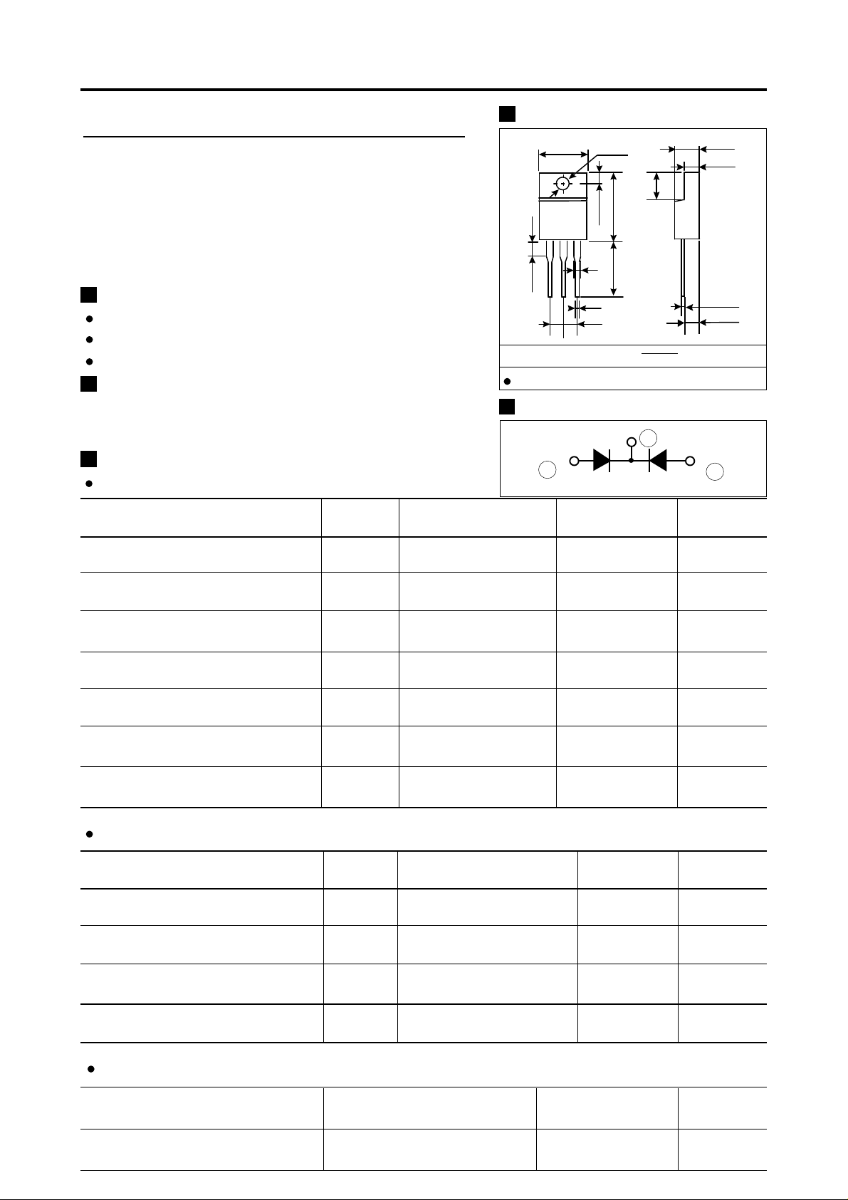
Outline Drawings
10±0.5
3.7±0.2
JEDEC
EIAJ
ø3.2
2.7±0.2
1.2±0.2
0.7±0.2
2.54±0.2
15±0.3
13Min
+0.2
-0.1
6.3
SC-67
Connection Diagram
2
1
Rating
4.5±0.2
2.7±0.2
+0.2
0.6
-0
2.7±0.2
3
Unit
V
Repetitive Peak Reverse Voltage
Repetitive Peak Surge Reverse Voltage
Isolation Voltage
Average Output Current
Surge Current
Operating Junction Temperature
Storage T emper ature
RRM
VRSM
Viso
IO
IFSM
Tj
Tstg
Terminals to Case,
AC. 1min.
duty=1/2, Tc=115°C
Square wave
Sine wave 10ms
Electrical Characteristics (Ta=25°C Unless otherwise specified )
Item
Forward V oltage Drop **
Reverse Current **
Symbol
V
F
IR
Conditions
IF=5A
VR=VRRM
200
200
1500
10*
50
-40 to +150
-40 to +150
V
V
V
A
A
°C
°C
* Out put current of centertap full wave connection.
Max.
0.95
100
Unit
V
µA
Reverse recovery time
Thermal Resistance
Mechanical Characteristics
Mounting torque
Weight
trr
Rth(j-c)
IF=0.1A,IR=0.2A,Irec=0.05A
Junction to case
Recommended torque
35
3.5
0.3 to 0.5
2.3
ns
°C/W
** Rating per element
N · m
g
(200V / 10A TO-22OF15)
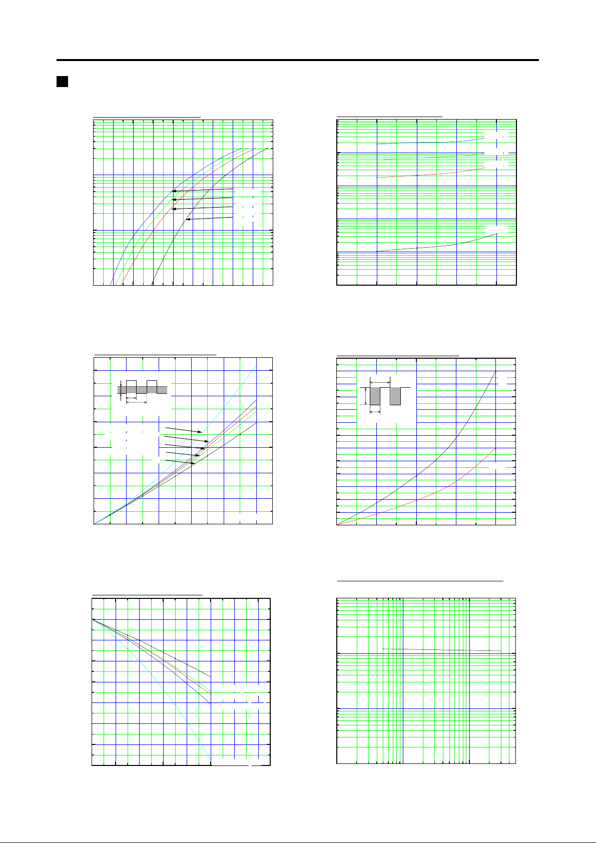
Characteristics
YG902C2R
Forward Characteristic (typ.)
100
10
Tj=150oC
Tj=125oC
Tj=100oC
1
Tj=25oC
IF Forward Current (A)
0.1
0.3 0.4 0.5 0.6 0.7 0.8 0.9 1.0 1.1 1.2
VF Forward Voltage (V)
Forward Power Dissipation
6
5
4
3
2
1
WF Forward Power Dissipation (W)
0
Io
λ
360°
DC
o
o
o
o
Per 1element
Square wave λ=60
Square wave λ=120
Sine wave λ=180
Square wave λ=180
012345
Io Average Forward Current (A)
Reverse Characteristic (typ.)
4
10
3
10
A)
µ
2
10
1
10
0
10
IR Reverse Current (
-1
10
0 50 100 150 200
VR Reverse Voltage (V)
Reverse Power Dissipation
1.3
1.2
1.1
1.0
0.9
0.8
0.7
0.6
0.5
0.4
0.3
0.2
0.1
PR Reverse Power Dissipation (W)
0.0
0 50 100 150 200
360°
VR
α
VR Reverse Voltage (V)
Tj=150oC
Tj=125oC
Tj=100oC
Tj= 25oC
DC
=180
α
o
Current Derating (Io-Tc)
160
150
140
C)
o
130
120
110
100
90
Tc Case Temperature (
80
0 2 4 6 8 10 12 14
Io Average Output Current (A)
:Conduction angle of forward current for each rectifier element
λ
Io:Output current of center-tap full wave connection
DC
Square wave λ=180
Sine wave λ=180
Square wave λ=120
Square wave λ=60
o
Junction Capacitance Characteristic
(typ.)
100
10
o
o
o
1
Cj Junction Capacitance (pF)
0.1
1 10 100
VR Reverse Voltage (V)
 Loading...