

Page 1
Code Mercenaries
1
IIIIOO
OO
WW
WW
55
55
66
66----
DD
DD
GG
GG
1. Features
• USB interface
• USB V1.1/2.0 full speed device
• 50, 100, or 400 kHz I2C (IIC / TWI) master
• SPI master up to 8 MBit/sec
• Throughput up to 60 kbyte/s
• Based on IO-Warrior56
• Supports clock stretching on I2C
• Multi master capable I2C
• 5 V and 3.3 V available for external circuit
• Uses standard system drivers
• Standard form factor, no blocked ports
• Extended temperature: -10 to +85°C
1.1 Variants
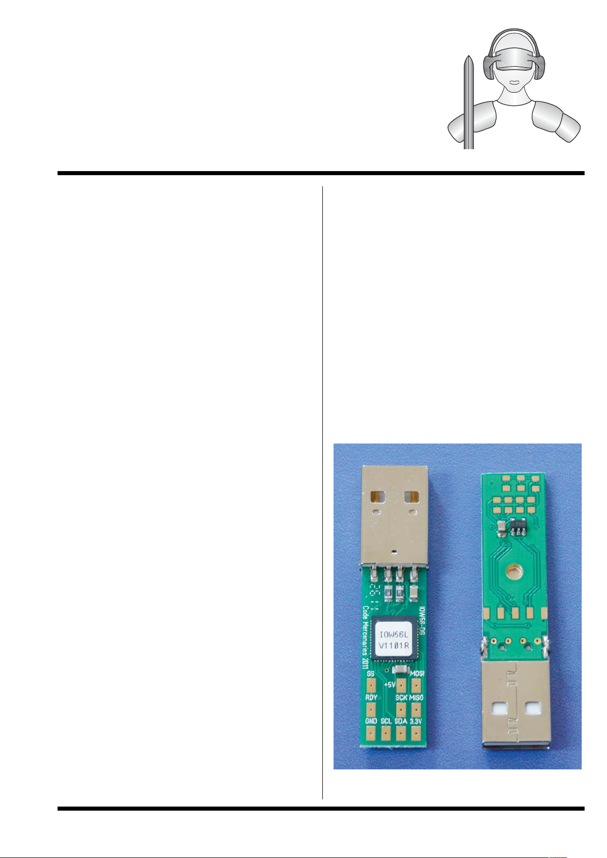
The standard IOW56-DG is shipped as a kit
containing an assembled and tested PCB, a two
part dongle case, and a ten wire cable to solder to
the dongle as required for the target application.
1.2 Custom variants
OEM versions with specialized cables or custom
modifications are possible
2. Functional overview
IOW56-DG packages a standard IO-Warrior56 in a
small form factor dongle case with a 3.3 V voltage
regulator.
The SPI and I2C signals of the IO-Warrior56 are
made available externally through solder pads to
allow application specific cabling to be attached.
All software and tools for IO-Warrior56 are also
usable for the dongle.
The I2C interface works as a bus master, supports
clock stretching handshake and multi master
configurations.
SPI works as a master with clock rates up to 8
MHz (cable length may be critical at higher clock
rates).
For compatibility with low voltage slaves the
internal pull up resistors of IOW56 can be
switched off by software command. Pull up control
is independent for SPI and I2C.
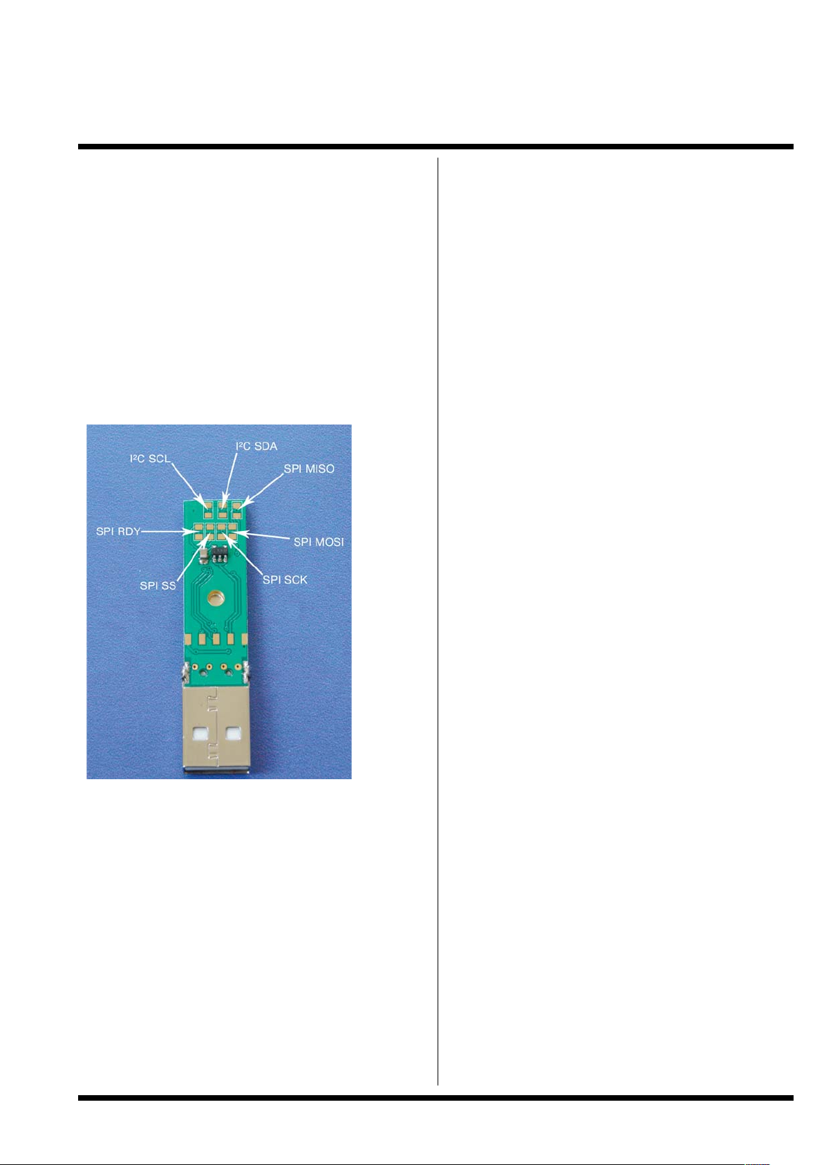
3. Connecting the cable
The function of the signals is marked on the board
next to the solder pads for the cable:
SS SPI - Slave Select, active low
+5 5V from USB, max. 100 mA
MOSI SPI - Master Out Slave In
RDY SPI - /DRDY
SCK SPI - Serial clock
MISO SPI - Master In Slave Out
GND Ground
SDA I2C SDA signal
SCL I2C SCL signal
3.3 3.3V output, max. 50 mA
Solder the cable to the pads as required for your
application.
The 5 V and 3.3 V supplies are meant to be used
exclusive of each other. If both are used at the
same time the combined current may not exceed
100 mA.
Dongle shown from both sides.
V1.0.1 October 6th 2012
USB to SPI and I2C Dongle
based on IO-Warrior56
Page 2
Code Mercenaries
2
IIIIOO
OO
WW
WW
55
55
66
66----
DD
DD
GG
GG
3.1 Compatibility with 3.3 V slaves
If a 3.3 V slave is to be connected the internal pull
up resistors of the IOW56 should be switched off
by software on enabling the I2C or SPI function.
This requires external pull up resistors which may
be added either on the slave side or soldered to the
lower side of the dongle PCB. It is recommended
to add protection diodes so the slave does not get
exposed to 5 V on the signal lines before the SPI or
I2C function of the IOW56 is initialized.
There are landing pads for pull up resistors
connecting to 3.3 V on the lower side of the dongle
PCB
3.2 Pull Up resistor positions
4. Software/Programming support
The IO-Warrior SDK is used with the dongle. The
SDK, additional software, and the data sheet for
the IOW56 are available on our website.
5. FCC / CE
The IOW56-DG is sold as kit. As such it can not be
FCC or CE approved.
Code Mercenaries has excerted greatest care in
designing this module to minimize RF emission
and assure stable operation. Though the use of
proper cable materials and correct integration into
a device is crucial to assure product safety and
interference free operation.
The integrator who assembles the module into a
device has to take care for appropriate testing and
safety measures.
6. Ordering information
The standard packaging for IOW56-DG is a blister
pack containing the parts for one unit.
The order code is:
IOW56-DG
Bulk packs with the parts for 10 units in a bag are
availabe under the order code:
IOW56-DG10
Legal Stuff
This document is ©1999-2012 by Code
Mercenaries.
The information contained herein is subject to
change without notice. Code Mercenaries makes
no claims as to the completeness or correctness of
the information contained in this document.
Code Mercenaries assumes no responsibility for
the use of any circuitry other than circuitry
embodied in a Code Mercenaries product. Nor
does it convey or imply any license under patent or
other rights.
Code Mercenaries products may not be used in any
medical apparatus or other technical products that
are critical for the functioning of lifesaving or
supporting systems. We define these systems as
such that in the case of failure may lead to the
death or injury of a person. Incorporation in such a
system requires the explicit written permission of
the president of Code Mercenaries.
Trademarks used in this document are properties of
their respective owners.
Code Mercenaries
Hard- und Software GmbH
Karl-Marx-Str. 147a
12529 Schönefeld OT Grossziethen
Germany
Tel: x49-3379-20509-20
Fax: x49-3379-20509-30
Mail: support@codemercs.com
Web: www.codemercs.com
HRB 9868 CB
Geschäftsführer: Guido Körber, Christian Lucht
V1.0.1 October 6th 2012
Page 3
Code Mercenaries
1
IIIIOO
OO----
WW
WW
aa
aarrrrrrrriiii
oo
oorrrr
55
55
66
66
1. Features
• Full speed USB interface (12MBit/sec)
• Full USB V2.0 compliant full speed device
• Full USB HID 1.1 compliance
• 50 general purpose I/O pins
• IIC master with 50, 100, or 400kbit/sec, multi
master capable
• Supports a wide range of alphanumeric and
graphic LCD modules
• SPI master up to 8MBit/sec
• Drives a LED matrix up to 8x64 with external
shift registers
• Drives a 8x8 key or switch matrix
• Easy to use starter kit
• Software support for Mac(10.2 and up), Linux
(Kernel 2.6), and Windows (XP and up)
• No USB knowledge necessary to use
• Single +5V power supply
• Available in MLFP56 package or 100mil spaced
through hole module.
• Extended temperature range: -40°C to +85°C
1.1 Variants
Right now the IO-Warrior chip family is available
in three low speed and one full speed variant.
This data sheet describes the full speed variant
IOW56.
For the low speed IO-Warrior chips please refer to
the separate data sheet.
1.2 Custom variants
Custom adaptions are available on request.
1.3 Supported OSes
WinXP and later
Compatibility with older Windows version is not
tested and no support available for those
Linux kernel 2.6 and up
MacOS X 10.3 and up
2. Functional overview
IO-Warrior offers a simple access to the USB.
Many projects that formerly used the parallel port
or some other kind of direct I/O interface today
face the problem that getting simple things to work
on the USB is quite complex.
With a serial or parallel port you needed only a
simple circuit to control an external relay or read a
single switch.
With USB you need a microcontroller that handles
all the protocol work to do the same thing. Several
standard commands need to be supported to get a
device accepted as a USB device, let alone
implementing any real function.
IO-Warrior brings simplicity to the USB. The
protocol is encapsulated in the IO-Warrior Chip.
You only have to care about the I/O pins and have
to write only a few simple lines of code to access
them.
IO-Warrior also supports a range of industrial
standard interfaces to simplify interfacing to
certain chips or modules. These interfaces are
handled internally in IO-Warrior removing the
bandwith wasting controlling of individual pins.
V 1.0.3, November 6nd 2012 for chip version V1.1.0.1
Generic universal I/O Controller
for USB
Page 4

Code Mercenaries
2
IIIIOO
OO----
WW
WW
aa
aarrrrrrrriiii
oo
oorrrr
55
55
66
66
2.1 Product selection matrix
2.2 Starter Kits
With the IO-Warrior Starter Kits you can make your first steps with IO-Warrior 56. A few elements on the
kit allow first experiments with inputs and outputs, the bread board area provides space to test your
individual circuit.
The starter kits are sold unassembled. A few minutes soldering will provide you with a working unit.
Actual components supplied with the kit may vary from those shown here.
Type USB Speed I/O Pins LCD IIC SPI RC5 IR Keys LEDs Timer SSOP48 DIL24 SOIC24 MLFP56 Module
IO-Warrior40
IO-Warrior24
low
low
32
16
8x16 8x32
8x32
IO-Warrior56 full 50 8x8 8x64
V 1.0.3, November 6nd 2012 for chip version V1.1.0.1
Page 5
Code Mercenaries
3
IIIIOO
OO----
WW
WW
aa
aarrrrrrrriiii
oo
oorrrr
55
55
66
66
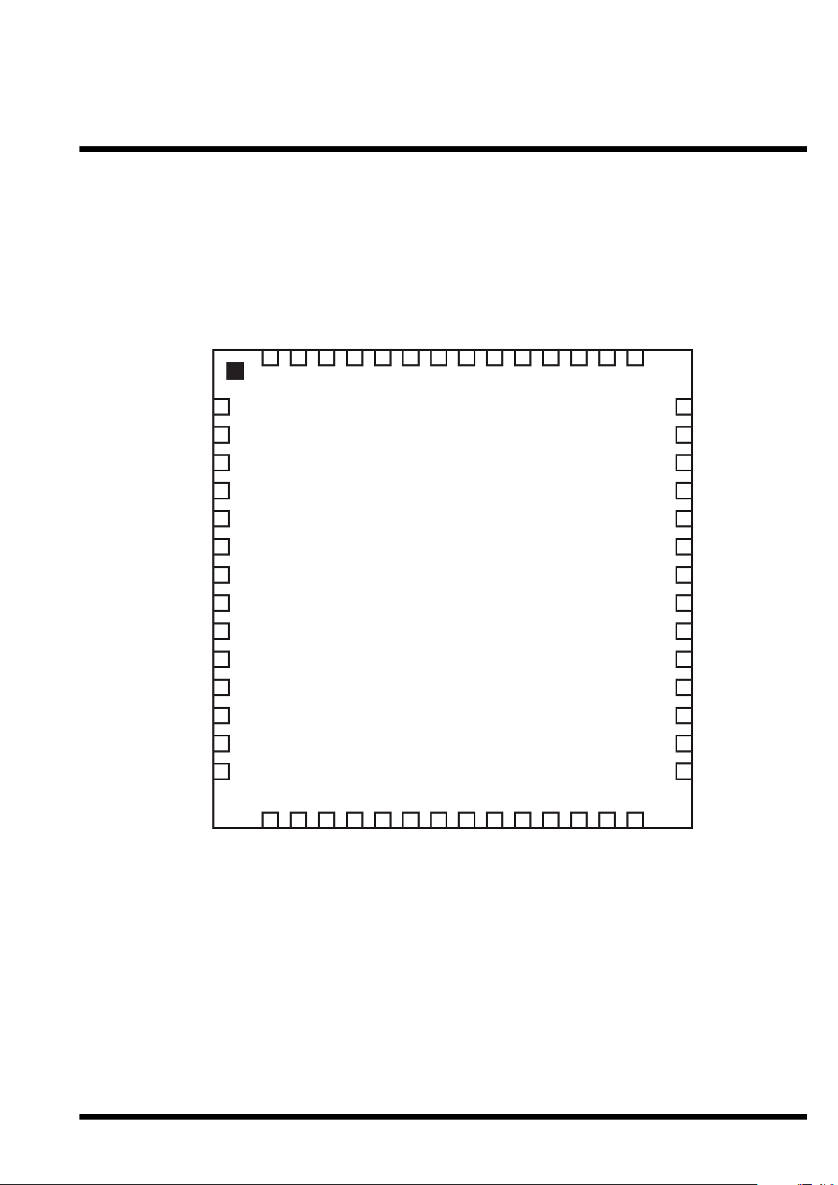
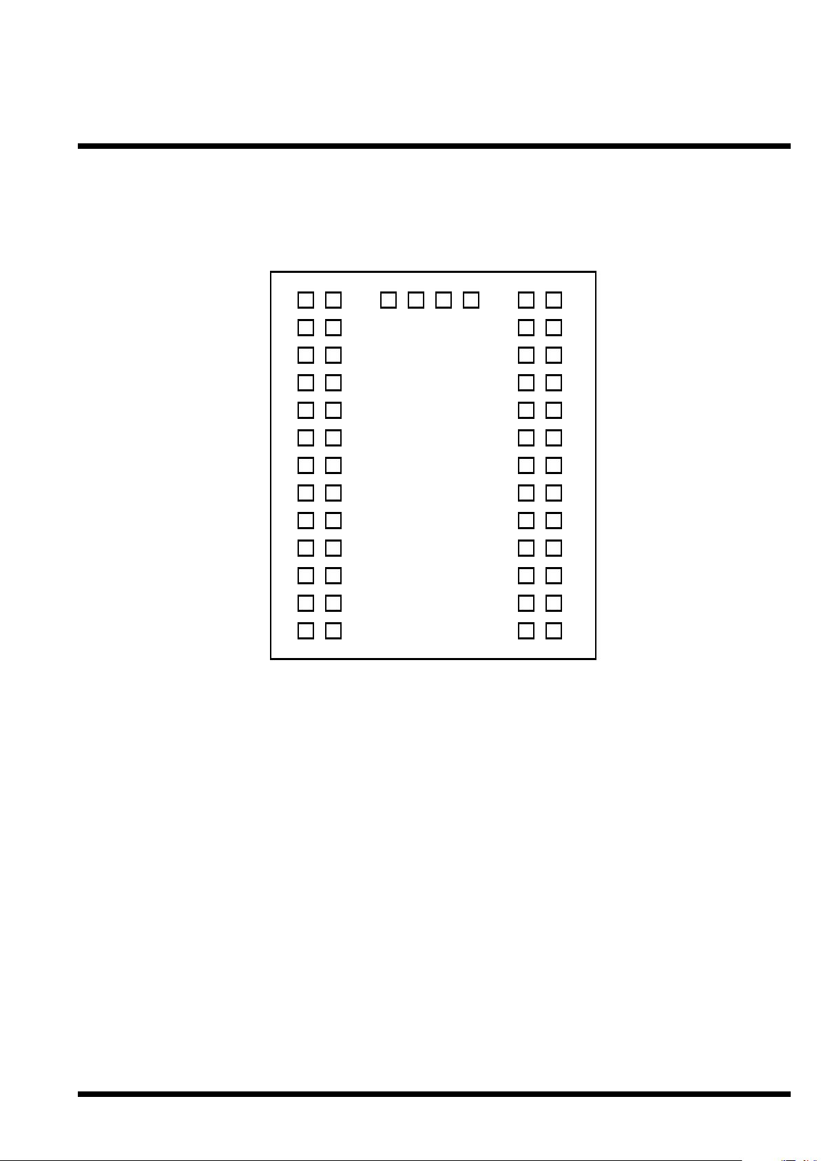
3.0 Pin Configurations
IO-Warrior56-LFXI
MLFP56 Package
All drawings: TOP VIEW!
V 1.0.3, November 6nd 2012 for chip version V1.1.0.1
P2.3
P2.5
P2.7
P0.1
56
55
54
1
P0.3
P0.5
53
525051
P0.7
Gnd
Vcc
P0.6
49
48
P0.4
47
P0.2
46
P0.0
45
P2.6
44
P2.4
43
42
P2.2
P2.1
P4.7
P4.5
P4.3
P4.1
P3.7
P3.5
P3.3
P3.1
P5.7
P5.5
P5.3
P5.1
10
11
12
13
14
2
3
4
5
6
7
8
9
15
16
17
18
192120
22
23
24
25
26
27
41
40
39
38
37
36
35
34
33
32
31
30
29
28
P2.0
P4.6
P4.4
P4.2
P4.0
P3.6
P3.4
P3.2
P3.0
P5.6
P5.4
P5.2
P5.0
P1.7
P1.5
D-
D+
P1.3
Gnd
P1.1
Vcc
P6.7
P6.0
P1.0
P1.2
P1.4
P1.6
Page 6
Code Mercenaries
4
IIIIOO
OO----
WW
WW
aa
aarrrrrrrriiii
oo
oorrrr
55
55
66
66
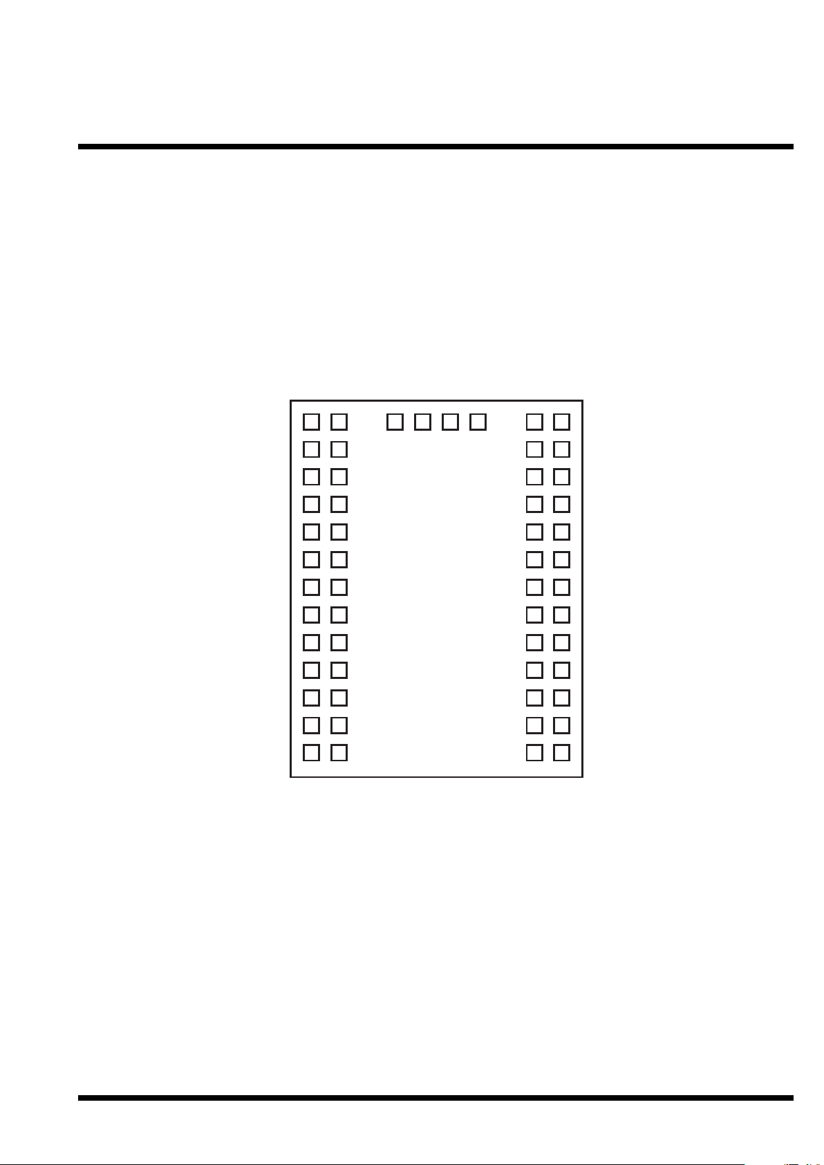
IO-Warrior56-MOD
Module
Pin numbers
All drawings: TOP VIEW!
1234
56
78
910
11 12
13 14
15 16
17 18
19 20
21 22
23 24
25 26
27 28
29 30 3132
3334
3536
3738
3940
4142
4344
4546
4748
4950
5152
5354
5556
V 1.0.3, November 6nd 2012 for chip version V1.1.0.1
Page 7
Code Mercenaries
5
IIIIOO
OO----
WW
WW
aa
aarrrrrrrriiii
oo
oorrrr
55
55
66
66
IO-Warrior56-MOD
Module
Pin names
All drawings: TOP VIEW!
V 1.0.3, November 6nd 2012 for chip version V1.1.0.1
P1.5
P5.1
P5.5
P3.1
P3.5
P4.1
P4.5
P2.1
P2.5
P0.1
P0.5
P0.6
NC
P1.3
P1.7
P5.3
P5.7
P3.3
P3.7
P4.3
P4.7
P2.3
P2.7
P0.3
P0.7
NC
GndD-D+
Vcc
P1.0
P1.2
P1.6
P5.2
P5.6
P3.2
P3.6
P4.2
P4.6
P2.2
P2.6
P0.2
P6.7
P6.0
P1.1
P1.4
P5.0
P5.4
P3.0
P3.4
P4.0
P4.4
P2.0
P2.4
P0.0
P0.4
Page 8

Code Mercenaries
6
IIIIOO
OO----
WW
WW
aa
aarrrrrrrriiii
oo
oorrrr
55
55
66
66
4.0 Pin Assignments IO-Warrior56
Pi # MLFP56 Pin# Module Type Name Special function
1
2
22
19
I/O
I/O
P2.3
P2.1X3X2
3
4
5
6
20
17
I/O
I/O
18
15
I/O
I/O
P4.7
P4.5 LCD-CS1 (not driven by special mode function)
P4.3
P4.1
LCD-E-/RE
LCD-RS
7
8
9
10
16
13
I/O
I/O
14
11
I/O
I/O
11
12
13
14
12
9
I/O
I/O
10
7
I/O
I/O
P3.7
P3.5
LCD-Data7
LCD-Data5
P3.3
P3.1
LCD-Data3
LCD-Data1
P5.7
P5.5
P5.3
P5.1
SPI-/DRDY
SPI-/SS
15
16
17
18
8
5
I/O
I/O
6
53
I/O
I/O
19
20
21
22
4
3
power
USB
2
1
USB
power
P1.7
P1.5
IIC-SCL
IIC-SDA
P1.3
P1.1
LED-/OE
LED-Clk, undefined state during start up
Gnd
D+
DVcc
23
24
25
26
56
55
I/O
I/O
54
52
I/O
I/O
27
28
29
30
51
50
I/O
I/O
49
48
I/O
I/O
P6.7
P6.0 Power select during start up
P1.0
P1.2
LED-Data, undefined state during start up
LED-Strobe
P1.4
P1.6
P5.0
P5.2
SPI-SCK
SPI-MOSI
31
32
33
34
47
46
I/O
I/O
45
44
I/O
I/O
35
36
37
38
43
42
I/O
I/O
41
40
I/O
I/O
P5.4
P5.6
SPI-MISO
P3.0
P3.2
LCD-Data0
LCD-Data2
P3.4
P3.6
LCD-Data4
LCD-Data6
P4.0
P4.2
LCD-/On
LCD-R/W-/WE
39
40
41
42
39
38
I/O
I/O
37
36
I/O
I/O
43
44
45
46
35
34
I/O
I/O
33
32
I/O
I/O
P4.4
P4.6
LCD-E2-/RES
LCD-CS2 (not driven by special mode function)
P2.0
P2.2X0X2
P2.4
P2.6X4X6
P0.0
P0.2Y0Y2
47
48
49
50
31
27
I/O
I/O
-
-
power
power
51
52
53
54
28
25
I/O
I/O
26
23
I/O
I/O
P0.4
P0.6Y4Y6
Vcc
Gnd
P0.7
P0.5Y7Y5
P0.3
P0.1Y3Y1
55
56
24
21
I/O
I/O
P2.7
P2.5X7X5
V 1.0.3, November 6nd 2012 for chip version V1.1.0.1
Page 9
Code Mercenaries
7
IIIIOO
OO----
WW
WW
aa
aarrrrrrrriiii
oo
oorrrr
55
55
66
66
4.1 Pin descriptions
D+, D-
Differential data lines of USB. Put 24 series
resistors in these lines and connect them to the
USB cable or plug, see application circuit for
details. The IOW56-MOD already has the series
resistors.
For a PCB layout make sure to run these two
signals next to each other. USB data is a
differential signal that produces best signal quality
and lowest RF emission if the two lines are close to
each other.
P0.0..P0.7
First I/O port of the chip. These pins correspond
with the lowest 8 bits of the input or output (bits
0..7).
P1.0..P1.7
Second I/O Port. Corresponds to the bits 8..15.
P1.0 and P1.1 are used during production of the
IOW56. After power up and during the internal
start up process of IOW56 these two pins can
change their status a couple times. Take this into
account when connecting external circuits.
P2.0..P2.7
Third I/O Port. Corresponds to the bits 16..23.
P3.0..P3.7
Fourth I/O Port. Corresponds to the bits 24..31.
P4.0..P4.7
Fifth I/O Port. Corresponds to the bits 32..39.
P5.0..P5.7
Sixth I/O Port. Corresponds to the bits 40..47.
P6.0, P6.7
Seventh I/O Port. Corresponds to the bits 48 and
55. This port has only two pins. Always write the
unused bits as "1".
GND
Power supply ground.
Vcc
Supply voltage.
A 100nF ceramic capacitor is required to be
connected directly to each pair of the power supply
pins. The IOW56-MOD already has the capacitors.
The MLFP56 package has a center ground pad that
must be connected to ground (Vss).
4.2 Special mode pin functions
IO-Warrior56 supports various higher level
functions including IIC, SPI, LED matrix, key
matrix, and driving various LCD modules.
Handling IIC via the normal generic I/O would be
very slow as each edge of data and clock would
have to be transmitted separately. At a rate of 1000
such transactions per second (which is the
maximum IO-Warrior56 is allowed by USB
specifications) the maximum bit rate and
throughput would be around 250 bits/sec.
To make IIC and other devices usable IO-Warrior
implements the special mode functions. By
handling the IIC inside IO-Warrior the actual data
rate is approaching the theoretical maximum.
When any of the special mode functions is
activated the corresponding pins will no longer
respond as generic I/O pins but are under control of
the activated special mode function.
4.2.1 IIC Mode pins
IO-Warrior56 can act as an IIC master with 50,
100, or 400kbit/sec data rate. Multi master mode is
supported.
IO-Warrior56 supports clock stretching handshake
with slaves that need throttling of the data flow.
The following pins get reassigned when the IIC
function is enabled:
These pins will no longer be affected by the data
sent via the normal port setting command. Both
pins have internal pull up resistors and open drain
drivers. They can be connected direct to IIC
compatible chips. Optionally the internal pull up
resistors can be disabled by setting the appropriate
flag in the IICenable command. This allows
operation with lower voltage IIC slaves.
Function IOW56
SCL
SDA
P1.7
P1.5
V 1.0.3, November 6nd 2012 for chip version V1.1.0.1
Page 10

Code Mercenaries
8
IIIIOO
OO----
WW
WW
aa
aarrrrrrrriiii
oo
oorrrr
55
55
66
66
4.2.2 LCD Mode pins
IO-Warrior56 has support for controlling LCD
modules with a wide range of controllers. Refer to
Application Note 5: "Controlling LCDs with IOWarrior" for more information on compatible
modules and how to use them.
The following pins get reassigned when the LCD
function is enabled:
When the LCD function is enabled these pins will
no longer be affected by the normal port setting
command.
/On should be used to enable power supply to LCD
modules that have high current demand or
backlighting. The /On signal is low when the LCD
function is enabled, it does go high when IOWarrior enters suspend mode or when the LCD
function is disabled.
By default the follwing pins should be used for
controlling the CS lines of graphic displays with
multiple controller chips:
P4.5 - CS1
P4.6 - CS2
Since the polarity of the CS signals varies between
LCD modules we decided not to handle them in the
special mode function.
The internal pull up resistors of the LCD signal
pins can be disabled by setting the appropriate flag
when enabling the LCD function. This allows IOWarrior56 to work with displays that use lower
supply voltage levels.
4.2.3 SPI Mode Pins
IO-Warrior56 has a hardware SPI master interface.
It can communicate with SPI slave devices with a
data clock speed of up to 8MHz. Actual data
throughput depends on a number of factors,
including the size of the data packets that are
transmitted. Possible peak rates are around 62,000
bytes/sec.
The following pins get reassigned when the SPI
function is enabled:
When the SPI function is enabled these pins will
no longer be affected by the normal port setting
command. The driver mode of the pins changes
when SPI is enabled.
SCK and MOSI use CMOS drivers, /SS open drain
with internal pull up, /DRDY is an input with
internal pull up and MISO is high Z input.
Optionally the pins can be switched to open drain
without pull up for /SS, MOSI, SCK and high Z
inputs for MISO and /DRDY. This allows
compatibility with devices that use a lower supply
voltage.
4.2.4 LED Matrix Mode Pins
IO-Warrior56 supports driving a LED matrix with
up to 8x64 LEDs.
When the LED Matrix function is enabled these
pins will no longer be affected by the normal port
setting command.
/OE is driven high when IO-Warrior enters the
suspend mode. The external driver should then
disable to stay within the USB power limits for
suspend mode.
For more details on how to control a LED matrix
please refer to the separate application note.
Function IOW56
/On
RS
P4.0
P4.1
R/W/WE
E/RE
E2/RES
Data0
P4.2
P4.3
P4.4
P3.0
Data1
Data2
Data3
Data4
P3.1
P3.2
P3.3
P3.4
Data5
Data6
Data7
P3.5
P3.6
P3.7
Function IOW56 Pin mode
/DRDY
/SS
P5.3
P5.1
int. pull up / high Z
open drain
MOSI
MISO
SCK
P5.2
P5.4
CMOS or open drain
high Z / input
P5.0 CMOS or open drain
Function IOW56
/OE
Strb
P1.3
P1.2
Clk
Data
P1.1
P1.0
V 1.0.3, November 6nd 2012 for chip version V1.1.0.1
Page 11

Code Mercenaries
9
IIIIOO
OO----
WW
WW
aa
aarrrrrrrriiii
oo
oorrrr
55
55
66
66
4.2.5 Switch Matrix Mode Pins
IO-Warrior56 supports scanning of a 8x8 matrix of
keys or switches. When this function is enabled
P0.0..7 will turn off their internal pull up resistors
and will be used as the Y lines that are periodically
driven to Gnd voltage level. P2.0..7 will serve as
the X matrix inputs, they will keep their internal
pull up resistors active so a closed switch in the
matrix will pull down the X line when the
corresponding Y line is driven low.
To allow more than two switches to be closed at
the same time and still be able to faultlessly detect
which of the matrix points are closed it is
necessary to insert a diode in series with every key
or switch in the matrix. The kathodes of the diodes
have to be connected to the Y lines (P0.0..7).
The following pins get reassigned when the key
mode is enabled:
The matrix is scanned every 4msec. Debounce
time is 16msec.
When IO-Warrior enters the suspend mode the X
and Y lines will be pulled high by internal pull up
resistors. Closing a switch/key does not wake the
IO-Warrior.
Function IOW56
X0
X1
P2.0
P2.1
X2
X3
X4
X5
P2.2
P2.3
P2.4
P2.5
X6
X7
Y0
Y1
P2.6
P2.7
P0.0
P0.1
Y2
Y3
Y4
Y5
P0.2
P0.3
P0.4
P0.5
Y6
Y7
P0.6
P0.7
V 1.0.3, November 6nd 2012 for chip version V1.1.0.1
Page 12

Code Mercenaries
10
IIIIOO
OO----
WW
WW
aa
aarrrrrrrriiii
oo
oorrrr
55
55
66
66
5.Device Operation
Due to the fact that all current operating systems
offer an especially easy access to devices in the
HID class, IO-Warrior was designed as a generic
HID device.
By identifying as a generic HID class device IOWarrior avoids being controlled by any of the
higher level system drivers, which makes it
possible to access IO-Warrior from application
level.
5.1 Accessing IO-Warrior
A common misconception with USB is to think
you can "talk to the USB port". The truth is that
you do that as likely as you are going to directly
talk to your Ethernet port or PCI bus.
Communication on the USB is always with a
specific device attached to the USB. The USB
itself is only the medium through which you
communicate.
To get access to a certain device you have to look
for the VendorID and ProductID of that device.
The specific mechanisms for doing so depend on
the individual operating system.
For details please refer to our sample code in the
SDK.
5.2 IO-Warrior communication
IO-Warrior56 has five USB endpoints. Endpoints
are like virtual communication ports into or out of
the device.
An endpoint can be assigned to an interface.
Interfaces are like virtual devices or subsystems
within a device. IO-Warrior uses interface 0 to talk
to the pins directly and interface 1 to talk to the
special mode functions.
Endpoint 0 is a standard endpoint that is present on
all USB devices. It does use the control transfer
mode and is used by the system to get information
about the device and to configure the device.
Endpoint zero can also be used to send data to the
devices functions. The low speed IO-Warrior chips
use Endpoint zero for output data, IO-Warrior56
has dedicated Endpoints for the output data to
achieve a higher performance.
For input data IO-Warrior is using endpoint 1 as an
interrupt-in endpoint. "Interrupt" is a bit
misleading in this case. For USB "interrupt" means
that data is sent when there is new data available.
The host computer is periodically asking the device
for new data. The device itself can not initiate the
data transfer. IO-Warrior sends a new report any
time it detects a change to the input pin status.
Output data to the I/O pins is send to Endpoint 2
which is also an interrupt type endpoint. A seven
byte report directly sets the status of the port pins.
Special mode functions receive their commands
via Endpoint 4, also interrupt mode. The report
size for the special mode functions is 63 bytes plus
the report ID. This enables a single IOW56 special
mode command to transport ten times more data
than on the low speed IO-Warrior chips.
Reactions to commands to the special mode
functions are sent via endpoint 3, also in interrupt
transfer mode.
Since IO-Warrior56 uses interrupt out endpoints it
can not be used with USB 1.0 hosts (i.e. Win98),
USB 1.1 is required as the minimum.
5.3 IO-Warrior input behaviour
IO-Warrior checks the status of all pins once every
millisecond. If it detects a change from the last
status a new report via endpoint 1 is issued. Pins
which are currently used by a special mode
function are not checked. Reports are send to the
computer in 1msec intervals.
The worst case latency from a status change to
sending off the report is 2 ms unless the operating
system adds additional latency.
5.4 IO-Warrior output behaviour
Upon receiving the report IO-Warrior writes the
new data to the output pins in groups of eight pins
each. Pins 0.0 to 0.7 get the new data first, then 1.0
to 1.7, 2.0 to 2.7, and last 6.0/ 6.7.
The time between the individual ports is about
1sec.
5.5 Using pins as inputs or outputs
All I/O pins on IO-Warrior can be used as input or
output pins.
All pins act as inputs all of the time. When
receiving an input report from IO-Warrior you
always get the current input status on all pins
except for those currently used by special mode
functions..
Writing a 0 as output value to any pin causes it to
drive the pin low with an open drain driver.
Usually this will result in this pin being read as a
zero input as well, unless so much current has to be
drained by the pin that the voltage remains above
the threshold level.
Writing a 1 to a pin causes the open drain driver to
be turned off. The pin will be pulled high by an
internal pull up resistor. Now the pin acts either as
an output with a high level, or can be used as an
input.
V 1.0.3, November 6nd 2012 for chip version V1.1.0.1
Page 13

Code Mercenaries
11
IIIIOO
OO----
WW
WW
aa
aarrrrrrrriiii
oo
oorrrr
55
55
66
66
5.6 Power supply
USB does allow a device to be "Bus Powered".
This means the device does get its power off the
USB port. To avoid overloading on the USB ports
devices need to advertise their power requirements.
There are two power classes for devices: Low
power and high power. Low power devices may
draw up to 100mA off the USB, high power
devices up to 500mA.
Likewise there are high power and low power
ports. Usually high power ports are those on the
motherboard and on hubs with external power
supply or hubs in a monitor. Low power ports are
typically on hubs that get their power off the USB,
like hubs in keyboards.
If the system decides that there is not sufficient
power to supply a high power decive that device
does not get enabled.
IO-Warrior56 can operate either as a high power or
low power device. Pulling the P6.0 pin high or low
at reset sets the desired power rating.
This allows to configure IO-Warrior56 optimally
for supporting external circuits.
5.7 Using external power
If an external power source is used to supply power
for an IO-Warrior56 based circuit there are two
options.
The IO-Warrior56 can be powered from the USB
and only the external circuit gets its power off an
external source. If this is a feasible design option it
should be used. An I/O pin may be used to check
the presence of the external power so any
controlling application knows if the device is in a
working configuration.
The second option is to also power IO-Warrior56
from an external source. This is not the
recommended option since IO-Warrior56 assumes
that the USB is active if it has power. In this case
set the current request of IO-Warrior56 to 100mA
5.8 Suspend
All devices on the USB port need to support the
suspended state. When the host computer stops to
periodically access the USB, like when it goes to
sleep, all devices need to enter the suspended state
and drop their power draw to less than 500A for
low power devices or less than 2.5mA for high
power devices.
When entering suspended state IO-Warrior56 pulls
all pins high. Care must be taken in designing
external circuits so that they will draw no more
than the allowed suspend power rating while all
pins of IO-Warrior56 are high.
5.9 Remote Wakeup
IO-Warrior56 chips support the remote wakeup
feature. They are able to wake the host computer
from sleep state if the host operating system has
enabled this feature.
Remote wakeup is initiated by IO-Warrior56 if any
pin changes its state while the chip is in suspended
state.
5.10 Special mode I/O
To enable IO-Warrior56 to talk to devices that
have more complex demands it has the special
mode functions. When any of these functions is
enabled some pins of IO-Warrior56 turn into
special function pins.
Talking to the special mode functions is handeled
via the USB interface 1, which is also configured
as generic HID compliant.
Commands to the special mode functions are sent
as interrupt out reports via endpoint 4. Replies
from the special mode functions are returned as
interrupt in reports via endpoint 3.
Endpoints 3 and 4 form the USB interface 1, or
pipe 1.
To talk to the various special mode functions and
to handle different requests to them ReportIDs are
used which enable multiple functions to use the
same endpoint. All reports to and from special
mode functions are always 64 bytes long, including
the ReportID.
The following chapters describe the individual
special mode functions.
V 1.0.3, November 6nd 2012 for chip version V1.1.0.1
Page 14

Code Mercenaries
12
IIIIOO
OO----
WW
WW
aa
aarrrrrrrriiii
oo
oorrrr
55
55
66
66
5.10.1 IIC Special mode function
The IIC function is enabled and disabled by
sending a report with the following structure with
ReportID=1 to interface 1:
enable=$01 enables the IIC function, $00 disables
it. Other values are reserved for future use.
Upon enabling IIC the SDA and SCL pins are
pulled high and are no longer under control of
interface 0. Disabling IIC does return the pins
under control of interface 0 and pulls them high
initially.
flags contains some configuration information:
7 - Disable Pull Ups (1 = disable)
6 - unused, write zero
5 - unused, write zero
4 - unused, write zero
3 - unused, write zero
2 - unused, write zero
1 - speed bit 1
0 - speed bit 0
Bit 7 "Disable Pull Up" allows operation with
external pull up resistors and lower voltage levels.
When this bit is set the internal pull up resistors of
the IIC pins are disabled and the SDA/SCL pins
work as open drain. The pull up resistors can not
be enabled again while the IIC function is active.
Disabling and again enabling the IIC function is
necessary to change the status of the pull-up
resistors back to active.
Bits 0 and 1, speed of the IIC clock.
0 = standard (93.75kHz)
1 = fast (375kHz)
2 = slow (46.8kHz)
A write request to the IIC is send with ReportID=2
and has the following format:
flags contains the following bits:
7 - Generate Start
6 - Generate Stop
5 - data count MSB
4 - data count
3 - data count
2 - data count
1 - data count
0 - data count LSB
If bit 7 - "Generate Start" is set a start signal (SDA
falling edge while SCL is high) is generated on the
IIC prior to sending out the first data byte.
Bit 6 - "Generate Stop" causes a stop signal (SDA
goes high while SCL is high) to be generated after
sending the last valid data byte of this report.
"data count" gives the number of valid data bytes
in the report. The number may range from 1 to 62,
higher values cause the report to be ignored.
To do write transactions that are longer than 62
bytes, send the first report with just the "Generate
Start" bit set, then send additional reports with
neither bit 6 or 7 set until the last report is send
which has the "Generate Stop" bit set.
Clock stretching by the slave to slow down data
transfer is supported by IO-Warrior56.
Sending just the address byte in write mode and
then terminating the transfer with a stop condition
is not supported by IOW56. Trying to send such a
command results in an error being returned. Errors
are returned also when another start condition is
attempted before issuing a stop, or if data is send
without having a valid start condition.
Any write transactions are acknowledged by a
report via interrupt-in endpoint 3:
flags contains the following bits:
7 - Error bit, 1 = error
6 - Arb loss bit, 1 = Arbitration lost
5 - data count MSB
4 - data count
3 - data count
2 - data count
1 - data count
0 - data count LSB
"data count" indicates the last byte that was
successfully transfered and acknowledged by the
slave (if any).
An error is indicated when the slave does not
acknowledge a transfer, or an invalid start/stop
condition was requested.
If another master starts transmission on the bus at
the same time and IO-Warrior56 loses the bus due
to a collision, an Arb Loss is returned.
To resolve an Arb Loss the transfer has to be
initiated again.
ReportID
$01 out
12
enable flags
34
$00 $00
... 62
$00 $0063$00
ReportID
$02 out
12
flags data
34
data data
... 62
data data63data
ReportID
$02 in
12
flags $00
34
$00 $00
... 62
$00 $0063$00
V 1.0.3, November 6nd 2012 for chip version V1.1.0.1
Page 15

Code Mercenaries
13
IIIIOO
OO----
WW
WW
aa
aarrrrrrrriiii
oo
oorrrr
55
55
66
66
Reading data off the IIC is initiated with a
ReportID=3. The initiating report has the following
format:
"command" holds the command byte to be send to
the IIC.
"count" is the number of bytes that should be read
off the IIC after sending the command byte, values
0 to 255 are valid, 0 reads 256 bytes.
A start signal is automatically generated before
sending the command byte and a stop is generated
after the last data byte is received. The read bit in
the address byte is automatically set to avoid bus
problems.
Data is returned in input reports with ID=3 via
endpoint 3. The data is returned in chunks of up to
62 bytes each with an error flag and byte count.
Multiple reports may be returned in reaction to a
read request:
flags contains the following bits:
7 - error, set if slave does not ack command byte
6 - Arb loss bit, 1 = Arbitration lost
5 - data count MSB
4 - data count
3 - data count
2 - data count
1 - data count
0 - data count LSB
Should the IIC slave fail to acknowledge the
command byte, the error flag will be set and the
transaction aborted. IIC does not have an error
condition during the actual reading of data after the
command byte was sent, except for the Arb Loss,
that can occur when another master starts a
transaction at the same time as the IO-Warrior56.
To resolve an Arb Loss the transfer has to be
initiated again.
Clock stretching by the slave to slow down data
transfer is supported by IO-Warrior56.
Multi master configurations are supported by IOWarrior56. If the bus is busy (a start was issued by
another master) IO-Warrior56 will wait for a stop
condition before it starts its IIC transaction. In the
case that another master starts using the bus at the
same time as IO-Warrior56 it is possible that an
Arbitration Loss is detected. This happens when
IO-Warrior56 is driving a logical high on SDA but
reads a low.
When that happens IO-Warrior56 will immediately
stop driving SDA but continues to drive SCK until
the end of the current byte and then returns an Arb
Loss error.
ReportID
$03 out
12
count command
34
$00 $00
... 62
$00 $0063$00
ReportID
$03 in
12
flags data
34
data data
... 62
data data63data
V 1.0.3, November 6nd 2012 for chip version V1.1.0.1
Page 16

Code Mercenaries
14
IIIIOO
OO----
WW
WW
aa
aarrrrrrrriiii
oo
oorrrr
55
55
66
66
5.10.2 LCD Special mode function
The LCD special mode function supports a wide
range of alphanumeric and graphic LCD modules.
The LCD function is enabled by sending an output
report with ID 4 to the USB interface 1:
enable = $00 disables the LCD function.
enable = $01 enables the LCD function, other
values are reserved.
"mode" contains a number of bits that determine
the behaviour of the LCD interface:
7 - Disable Pull Ups (1 = disable)
6 - unused, zero
5 - unused, zero
4 - LC7981
3 - T6963
2 - No44780Busy
1 - Reset
0 - Dual44780
"Dual44780" enables the second E signal to control
modules with two HD44780 controllers on them.
"No44780Busy" must be set for controllers that
don't have the busy flag in bit 7 of register 0 like
the HD44780 or KS0108 controllers. Setting this
flag does disable checking for the busy flag in bit 7
of the LCD register 0.
"Reset" enables the /RES pin. Upon issuing the
enable report with this bit set the LCD function
will pull the /RES pin low for approximately 2sec
before it is released to high again.
"T6963" switches to a mode compatible with the
T6963C controllers. Make sure to also set the
"No44780Busy" bit. The T6963 specific busy flags
are checked in this mode. The T6963C is the only
controller for which IOW56 implements the 8080
bus protocol.
"LC7981" switches to a mode compatible with the
LC7981 and HD61830 controllers. Make sure to
also set the "No44780Busy" bit. The LC7981
specific busy flag is checked in this mode.
Upon enabling the LCD function the Pins are put
under control of the LCD function and can no
longer be controlled by interface 0.
The /On pin is pulled low when the LCD function
is enabled, it will go high when the IO-Warrior56
enters suspend state.
To write data to the connected LCD module an
output report with ReportID 5 is written with the
following format:
"flags" contains the following bits:
7 - RS, Register Select bit
6 - Select Special
5 - data count MSB
4 - data count
3 - data count
2 - data count
1 - data count
0 - data count LSB
The status of the "RS" bit is used to set the RS or
A0 line to the LCD module.
With "data count" the number of bytes to be
written is specified. IO-Warrior56 will write up to
62 data bytes to the register specified by the "RS"
bit. If the "No44780Busy" flag has not been set the
Busy bit of the LCD module is automatically
checked and data written only when the LCD
module is ready to accept it.
When in "Dual44780" mode the "Select Special"
bit selects which of the E lines is used for this
request. "Select Special" = 0 uses E1, "Select
Special" = 1 uses E2.
In T6963 mode the "Select Special" bit selects if
the normal busy flag or the auto mode busy flag
should be checked. "Select Special" = 0 checks
STA0, 1 before writing to the LCD, "Select
Special" = 1 checks STA3.
ReportID
$04 out
12
enable mode
34
$00 $00
... 62
$00 $0063$00
ReportID
$05 out
12
flags data
34
data data
... 62
data data63data
V 1.0.3, November 6nd 2012 for chip version V1.1.0.1
Page 17

Code Mercenaries
15
IIIIOO
OO----
WW
WW
aa
aarrrrrrrriiii
oo
oorrrr
55
55
66
66
To read data from the LCD module an output
report with ID 6 is sent to interface 1:
"flags" contains the following bits:
7 - RS, Register Select bit
6 - Select special
5 - data count MSB
4 - data count
3 - data count
2 - data count
1 - data count
0 - data count LSB
"RS" specifies which register is to be accessed.
"data count" sets the number of bytes to be read off
the LCD.
When in "Dual44780" mode the "Select Special"
bit selects which of the E lines is used for this
request. "Select Special" = 0 uses E1, "Select
Special" = 1 uses E2.
In "T6963" mode the "Select Special" bit selects if
the normal busy flag or the auto mode busy flag
should be checked. "Select Special" = 0 checks
STA0, 1 before writing to the LCD, "Select
Special" = 1 checks STA2.
Up to 63 bytes can be read with one request. The
data read from the LCD module is returned in input
reports with ID 6:
"count" specifies the number of bytes returned in
this report. If more than 62 bytes are requested the
data will be returned in multiple reports.
Following is a list of the LCD controllers that have
by now been tested with IOW56 and the mode byte
that is used for them. Additional chip types will be
added when tested.
ReportID
$06 out
12
flags $00
34
$00 $00
... 62
$00 $0063$00
ReportID
$06 in
12
count data
34
data data
... 62
data data63data
Chip
HD44780
ST7920
mode
Remarks
$00 / $01
$00
mode = $01 for dual chip
HD61202
KS0108
S6B0108
S1D15xxx
SED152x
AX1520
NJU6450
S1D133xx
SED133x
T6963
$02
$02
May have two chips,
which means two CS
lines, either polarity
May have two chips, two
/CS lines, active low.
May require 18kHz clock
Superset of KS0108
$06
$0A
Select 6800 bus mode on
the module
May have a Font select
line
LC7981
HD61830
$16
V 1.0.3, November 6nd 2012 for chip version V1.1.0.1
Page 18

Code Mercenaries
16
IIIIOO
OO----
WW
WW
aa
aarrrrrrrriiii
oo
oorrrr
55
55
66
66
5.10.3 SPI Special mode function
IO-Warrior56 has a hardware SPI interface
enabling it to talk to many peripheral devices.
IOW56 supports SPI master mode.
To enable the SPI function a report with ID 8 is
sent to interface1:
"enable" = $00 disables the SPI and $01 enables it.
"mode" contains flags specifying the operating
mode for the SPI:
7 - LSBfirst
6 - unused, write zero
5 - unused, write zero
4 - unused, write zero
3 - unused, write zero
2 - CPHA
1 - CPOL
0 - unused, write zero
"LSBfirst" selects which bit of the data byte gets
shifted first. "LSBfirst" = 0 shifts MSB first,
"LSBfirst" = 1 shifts LSB first.
"CPHA" works together with "CPOL" to specify
which clock edges are used to drive and sample
data bits.
"CPOL" = 0 causes SCK to idle low between data
bytes," CPOL" = 1 makes SCK idle high.
"CPHA" = 0 causes data to be sampled on the first
clock edge and driven on the second edge.
"CPHA" = 1 causes data to be driven on the first
edge and sampled on the second edge (this is the
opposite behaviour of IOW24 CPHA bit).
Enabling SPI takes P5.0..P5.4 out of the control of
interface zero.
clock sets the clock divider. The master clock rate
is 24 MHz which is divided by clock+1. The valid
range for clock is 2 to 255. So the fastest SCLK
rate is 8MHz, the slowest 93.75kHz.
flags contains configuration bits.
7 - Disable Pull Ups (1 = disable)
6 - unused, write zero
5 - unused, write zero
4 - unused, write zero
3 - unused, write zero
2 - unused, write zero
1 - unused, write zero
0 - unused, write zero
SPI does always shift data in and out
simultaneously. So there is only one command to
send data out of SPI that does also result in the
same number of bytes being read in and returned to
the host. If the intention is to only read data from
an external device it is still necessary to shift out
the same number of dummy bytes to that device.
Data transfers on the SPI are initiated by a report
with ID 9:
"flags" contains the following bits:
7 - useDRDY, 1 = do handshake
6 - SSactive, 1 = /SS stays active
5 - ignoreDRDY, 1 = first byte ignores /DRDY
4 - unused, zero
3 - unused, zero
2 - unused, zero
1 - unused, zero
0 - unused, zero
"useDRDY" enables a handshaking signal that
allows the slave to signal if and when it is ready to
accept or send data.
If "useDRDY" = 1 IO-Warrior56 will check for the
/DRDY signal to be low before it starts shifting a
data byte. If the slave wants to pause the data
transmission it has to pull /DRDY high before the
end of the current byte transfer.
Upon starting a data transfer it may be desired to
send the first byte without the slave signalling /
DRDY low. By setting "ignoreDRDY" to 1 the
first byte of this report is sent to the slave without
checking /DRDY. Prior to shifting the next byte
IO-Warrior56 will check the status of /DRDY.
"count" has the number of bytes to shift, values 161 are valid, others will be ignored.
IO-Warrior56 assertes /SS before starting to shift
the first data byte of this report and will deassert it
after completing the last byte, unless bit 6
"SSactive" is = 1. If "SSactive" is set /SS will stay
asserted after the last byte of the report has been
transfered, allowing more than 61 bytes to take part
of a single transfer.
Data shifted in by IO-Warrior56 during a
transaction is returned in a report with ID 9:
"count" holds the number of valid bytes in the
report.
ReportID
$08 out
12
enable mode
34
clock flags
... 62
$00 $0063$00
ReportID
$09 out
12
count flags
34
data data
... 62
data data63data
ReportID
$09 in
12
count data
34
data data
... 62
data data63$00
V 1.0.3, November 6nd 2012 for chip version V1.1.0.1
Page 19

Code Mercenaries
17
IIIIOO
OO----
WW
WW
aa
aarrrrrrrriiii
oo
oorrrr
55
55
66
66
5.10.3.1 SPI CPHA / CPOL
If CPOL and CPHA are = 0 data is driven on the
falling edges of SCK (green lines) and sampled on
the rising edges (blue lines). The first bit is driven
before the first rising edge on SCK.
For CPOL = 0 and CPHA = 1 data is driven on the
rising edges of SCK (blue lines) and sampled on
the falling edges (green lines). The first bit is
driven on the first rising edge of SCK.
For CPOL = 1 and CPHA = 0 data is driven on the
rising edges of SCK (green lines) and sampled on
the falling edges (blue lines). The first bit is driven
before the first falling edge of SCK.
For CPOL = 1 and CPHA = 1data is driven on the
falling edges of SCK (blue lines) and sampled on
the rising edges (green lines). The first bit is driven
on the on the first falling edge of SCK.
V 1.0.3, November 6nd 2012 for chip version V1.1.0.1
Page 20

Code Mercenaries
18
IIIIOO
OO----
WW
WW
aa
aarrrrrrrriiii
oo
oorrrr
55
55
66
66
5.10.4 Driving a LED matrix
IO-Warrior56 has the capability to drive a matrix
of up to 8x64 LEDs with the aid of a few simple
external driver chips.
To enable the reciever function a report with ID
$14 is sent to interface 1:
enable = $01 enables the LED function, enable =
$00 disables it again.
Data to be displayed in the matrix is written in two
blocks of 32 bytes:
"block" = 0 writes to the first four lines, "block" =
1 to the second four lines.
5.10.5 Switch Matrix Mode
IO-Warrior56 can handle a matrix of 8x8 switches
or keys. Other than with a keyboard controller it is
possible to read out all possible combinations of
closed switches. Since the switch status is reported
as a bitmap there is no limitation to the number of
switches that can be closed at the same time
(diodes are required in the matrix though if more
than two keys can be pressed at the same time).
To enable the switch matrix function a report with
ID $18 is sent to interface 1:
"enable" = $01 enables the switch matrix function,
"enable" = $00 disables it again.
The status of the matrix is returned when ever there
is a change of status or it can be requested
immediately by sending a report with ID $19:
The status of the matrix is returned in an input
report with ID $19. A set bit denotes a closed
switch:
5.10.6 Getting special mode function status
To get the information which special modes are
currently in use, send a report with reportID $FE to
interface 1:
This will immediately return an input report with
ID $FE that contains flags for the special mode
functions. Non zero means the function is active:
5.10.7 Getting current pin status
Due to the way Windows implements HID support
IO-Warrior56 is unable to continuously send its
status.
HID class devices do have a function that allows
the host to set the rate at which reports should be
repeated if there is no change to the data. Windows
does set this rate to zero for IO-Warrior56, which
means IO-Warrior56 may send data only if there
are changes.
To be able to get the current status from IOWarrior56 it does support a Special Mode Function
that always returns the current status of all pins.
To get the port status just send a report with ID
$FF to interface 1:
This will result in the current pin status to be
returned immediately in an input report with ID
$FF with the following format:
ReportID
$14 out
12
enable $00
34
$00 $00
... 62
$00 $0063$00
ReportID
$15 out
12
block
data0
... 33
datan data31
34 ...
$00 $0063$00
ReportID
$18 out
12
enable $00
34
$00 $00
… 62
$00 $0063$00
ReportID
$19 out
12
$00 $00
34
$00 $00
… 62
$00 $0063$00
ReportID
$19 in
12
Y0 Y1
34
Y2 Y3
56
Y4 Y5
78
Y6 Y7
… 63
$00 $00
ReportID
$FE out
12
$00 $00
34
$00 $00
... 62
$00 $0063$00
ReportID
$FF in
12
IIC LCD
34
SPI LED
56
Key $00
... 63
$00 $00
ReportID
$FF out
12
$00 $00
34
$00 $00
... 62
$00 $0063$00
ReportID
$FF in
12
Prt0 Prt1
34
Prt2 Prt3
56
Prt4 Prt5
7 ...
Prt6 $00
V 1.0.3, November 6nd 2012 for chip version V1.1.0.1
Page 21

Code Mercenaries
19
IIIIOO
OO----
WW
WW
aa
aarrrrrrrriiii
oo
oorrrr
55
55
66
66
6. Absolute Maximum Ratings
Storage Temperature ........................................................................................-55°C to +100°C
Ambient Temperature with power applied.........................................................-40°C to +85°C
Ambient Temperature using USB ......................................................................-10°C to +85°C
Supply voltage on Vcc relative to Gnd ..................................................................-0.5V to +6V
DC input voltage....................................................................................Gnd-0.5V to Vcc+0.5V
Maximum current into any port pin..........................................................................-25/+50mA
Maximum combined output low current for all port pins ...............................................150mA
Static discharge voltage..................................................................................................>2000V
Latch-up current ..............................................................................................................200mA
6.1 DC Characteristics
Parameter Min Max Units Remarks
V
cc
I
cc
Operating Voltage
Operating Supply Current
4.35 5.25
50
V
mA Depending on operating mode
I
sb
I
ol
R
up
V
ith
Suspend mode current
Sink current on output pins
Pull-up Resistance
Input threshold voltage
4
45%
25
25
A
mA
8
65%
k
V
cc
Oscillator off
Vout = 0.75V
All ports, low to high edge
V
H
V
oh
V
ol
Input hysteresis voltage
USB Interface
6%
Static output high
Static output low
2.8
V
di
V
cm
V
se
C
in
Differential Input sensitivity
Differential Input common Mode Range
0.2
0.8
Single Ended Transceiver Threshold
Transceiver capacitance
0.8
12%
V
cc
3.6
0.3
VV15k±5% to GND
2.5
V
V
2.0
20
V
pF
|(D+)-(D-)|
R
ext
Z
o
V
Ccrs
External USB series resistor
USB driver output impedance
23
28
D+/D- crossover voltage 1.3
25
44
2.0 V
In series with each USB pin
Including R
ext
V 1.0.3, November 6nd 2012 for chip version V1.1.0.1
Page 22

Code Mercenaries
20
IIIIOO
OO----
WW
WW
aa
aarrrrrrrriiii
oo
oorrrr
55
55
66
66
7. Ordering information
The chips listed here are standard products.
Customized chips are available on request.
7.1 Packaging info
MLFP56 chips are packaged in trays with 250
chips each. Only complete trays are available due
to mechanical handling as well as moisture
sensitivity of the package.
IOW56-LFXI has MSL 3.
IOW56 modules are available in any quantity,
packaging units are 1 and 15.
7.2 USB VendorID and ProductID
By default all IO-Warrior chips are shipped with
the USB VendorID of Code Mercenaries ($7C0 or
decimal 1984) and a fixed ProductID.
On request chips can be equipped with the
customers VendorID and ProductID. VendorIDs
can be obtained from the USB Implementers
Forum <www.usb.org>
Customized chips may be subject to minimum
order quantities, contact <sales@codemercs.com>
for details.
Following are the ProductIDs for the IO-Warrior
controllers:
IO-Warrior56 $1503
ProductIDs are independent of the package type.
7.3 Serial numbers
All IO-Warrior chips do have unique serial
numbers in their device descriptors. These serial
numbers can be used to simplify programming for
multiple IO-Warriors connected to a single
computer.
The serial numbers are factory programmed and
can not be changed. Serial numbers are 8 digit
hexadecimal numbers. No two chips of a type will
be produced with identical serial numbers. Though
it can be that a IOW24 has the same serial number
as a IOW40 or IOW56 chip.
It is not possible to order chips with a specific
serial number unless they are ordered as custom
chips which are subject to minimum order volumes
and setup charges.
V 1.0.3, November 6nd 2012 for chip version V1.1.0.1
Partname Order Code Description Package
IO-Warrior56
IO-Warrior56
IOW56-LFXI
IOW56-MOD
IO-Warrior 50 I/O pins
IO-Warrior 50 I/O pins
MLFP56
Module
Page 23

Code Mercenaries
21
IIIIOO
OO----
WW
WW
aa
aarrrrrrrriiii
oo
oorrrr
55
55
66
66
8. IO-Warrior56 basic circuit(MLFP56 package)
GND
D+
D-
+5V
4
3
2
1
USB
P4.7
P4.6
P4.5
P4.4
P4.3
P4.2
P4.1
P4.0
P5.7
P5.6
P5.5
P5.4
P5.3
P5.2
P5.1
P5.0
P6.7
P6.0
D+
D-
P3.7
P3.6
P3.5
P3.4
P3.3
P3.2
P3.1
P3.0
P2.7
P2.6
P2.5
P2.4
P2.3
P2.2
P2.1
P2.0
P1.7
P1.6
P1.5
P1.4
P1.3
P1.2
P1.1
P1.0
P0.7
P0.6
P0.5
P0.4
P0.3
P0.2
P0.1
P0.0
IIIIOOOO----WWWWaaaarrrrrrrriiiioooorrrr 55556666----LLLLFFFFXXXXII
II
VccVcc
GNDGND
3
40
4
39
5
38
6
37
11
32
12
31
13
30
14
29
23
24
20
21
7
36
8
35
9
34
10
33
55
44
56
43
1
42
2
41
15
28
16
27
17
26
18
25
51
48
52
47
53
46
54
45
C2
100nF
C1
100nF
R1
24
R2
24
R3
100K
V 1.0.3, November 6nd 2012 for chip version V1.1.0.1
Page 24

Code Mercenaries
22
IIIIOO
OO----
WW
WW
aa
aarrrrrrrriiii
oo
oorrrr
55
55
66
66
8.1 IO-Warrior56 Starterkit Circuit
GND
D+
D-
+5V
4
3
2
1
USB
J1 R1
100K
470
R2
D1
J2
S1
10F
C1
P4.7
P4.6
P4.5
P4.4
P4.3
P4.2
P4.1
P4.0
P5.7
P5.6
P5.5
P5.4
P5.3
P5.2
P5.1
P5.0
P6.7
P6.0
D+
D-
P3.7
P3.6
P3.5
P3.4
P3.3
P3.2
P3.1
P3.0
P2.7
P2.6
P2.5
P2.4
P2.3
P2.2
P2.1
P2.0
P1.7
P1.6
P1.5
P1.4
P1.3
P1.2
P1.1
P1.0
P0.7
P0.6
P0.5
P0.4
P0.3
P0.2
P0.1
P0.0
IIIIOOOO----WWWWaaaarrrrrrrriiiioooorrrr 55556666----MMMMOOOODD
DD
Vcc
GND
20
38
17
39
18
40
15
41
12
46
9
47
10
48
7
49
56
55
3
2
16
42
13
43
14
44
11
45
24
34
21
35
22
36
19
37
8
50
5
51
6
52
53
54
28
27
25
31
26
32
23
33
V 1.0.3, November 6nd 2012 for chip version V1.1.0.1
Page 25

Code Mercenaries
23
IIIIOO
OO----
WW
WW
aa
aarrrrrrrriiii
oo
oorrrr
55
55
66
66
9. Package Dimensions
Module
The module contains the bypass capacitors as well as the USB series resistors.
V 1.0.3, November 6nd 2012 for chip version V1.1.0.1
Page 26

Code Mercenaries
24
IIIIOO
OO----
WW
WW
aa
aarrrrrrrriiii
oo
oorrrr
55
55
66
66
9.1 Package Dimensions
QFN 56
(Drawing from Cypress data sheet)
Center pad must be soldered to ground
V 1.0.3, November 6nd 2012 for chip version V1.1.0.1
Page 27

Code Mercenaries
25
IIIIOO
OO----
WW
WW
aa
aarrrrrrrriiii
oo
oorrrr
55
55
66
66
10. ESD Considerations
IO-Warrior56 has an internal ESD protection to
withstand discharges of more than 2000V without
permanent damage. However ESD may disrupt
normal operation of the chip and cause it to exhibit
erratic behaviour.
For the typical office environment the 2000V
protection is normally sufficient. Though for
industrial use additional measures may be
necessary.
When adding ESD protection to the signals special
care must be taken on the USB signal lines. The
USB has very low tolerance for additional
resistance or capacitance introduced on the USB
differential signals.
In any case the USB 2.0 specification chapter 6
and 7 should be read for detailed specification of
the electrical properties.
10.1 EMC Considerations
IO-Warrior uses relatively low power levels and so
it causes few EMC problems. The most important
issue is to provide a very clean layout for the
power supply. IO-Warrior56 runs at 24MHz
internal clock rate, this can cause current spikes if
the supply lines are not carefully layed out.
To avoid any EMC problems the following rules
should be followed:
• Keep the PCB traces from the resonator to the
chip pins as short as possible.
• Put the 100nF ceramic capacitors right next to
the power supply pins of the chip and make sure
the PCB traces between the chips power pins
and the capacitor are as short as possible.
• Run the power supply lines first to the capacitor,
then to the chip.
• Connect the second ground and supply pin in
the shortest possible way to the first ground and
supply pin. No other things may have
precedence over this.
• Keep the two USB signal lines close to each
other, route no other signal between them. USB
uses differential signalling so the best signal
quality with lowest RF emission is achieved by
putting these lines very close to each other.
11. Revision History
IO-Warrior56 does not use the same code base as
IO-Warrior24 and IO-Warrior40, so the version
numbers are not identical.
1.1.0.1
Feature release.
IIC multi master capability added.
Some invalid combinations on IIC now generate
errors, older versions could hang the IIC function
on violations of start/stop sequences.
Disabling pull-up resistors for low voltage
compatibility added to IIC, SPI, and LCD
functions.
1.1.0.0
Not released due to a bug.
1.0.0.2
Bugfix release. A problem in the USB stack was
fixed that had resulted in malfunctioning chips.
This was a production issue.
1.0.0.1
Initial release
1.0.0.0
Not released due to a bug.
V 1.0.3, November 6nd 2012 for chip version V1.1.0.1
Page 28

Code Mercenaries
26
IIIIOO
OO----
WW
WW
aa
aarrrrrrrriiii
oo
oorrrr
55
55
66
66
Legal Stuff
This document is ©1999-2012 by Code
Mercenaries.
The information contained herein is subject to
change without notice. Code Mercenaries makes
no claims as to the completeness or correctness of
the information contained in this document.
Code Mercenaries assumes no responsibility for
the use of any circuitry other than circuitry
embodied in a Code Mercenaries product. Nor
does it convey or imply any license under patent or
other rights.
Code Mercenaries products may not be used in any
medical apparatus or other technical products that
are critical for the functioning of lifesaving or
supporting systems. We define these systems as
such that in the case of failure may lead to the
death or injury of a person. Incorporation in such a
system requires the explicit written permission of
the president of Code Mercenaries.
Trademarks used in this document are properties of
their respective owners.
Code Mercenaries
Hard- und Software GmbH
Karl-Marx-Str. 147a
12529 Schönefeld OT Grossziethen
Germany
Tel: x49-3379-20509-20
Fax: x49-3379-20509-30
Mail: support@codemercs.com
Web: www.codemercs.com
HRB 9868 CB
Geschäftsführer: Guido Körber, Christian Lucht
V 1.0.3, November 6nd 2012 for chip version V1.1.0.1
 Loading...