

Page 1
Code Mercenaries
1
IIIIOO
OO
WW
WW
22
22
44
44----
DD
DD
GG
GG
1. Features
• USB interface
• USB V1.1/2.0 low speed device
• 100 kHz I2C (IIC / TWI) master
• Throughput up to 750 byte/s
• Based on IO-Warrior24
• Supports clock stretching
• Programmable timeout
• Supports Sensirion sensor protocol
• 5 V and 3.3 V available for external circuit
• Uses standard system drivers
• Standard form factor, no blocked ports
1.1 Variants
The standard IOW24-DG is shipped as a kit containing an assembled and tested PCB, a two part
dongle case, and a four wire cable to solder to the
dongle as required for the target application.
1.2 Custom variants
OEM versions with specialized cables or custom
modifications are possible
2. Functional overview
IOW24-DG packages a standard IO-Warrior24 in a
small form factor dongle case with a 3.3 V voltage
regulator.
The I2C signals of the IO-Warrior24 are made
available externally through solder pads to allow
application specific cabling to be attached. All software and tools for IO-Warrior24 are also usable for
the dongle.
The I2C interface works as a bus master and supports clock stretching handshake. A timeout can be
programmed to avoid hanging due to misbehaving
slaves.
For compatibility with low voltage slaves the internal pull up resistors of IOW24 can be switched off
by software command.
In addition to the standard I2C protocol the derivative protocol used by Sensirion to talk to their humidity sensors is also supported.
3. Connecting the cable
The function of the signals is marked on the board
next to the solder pads for the cable:
3.3 3.3V output, max. 50mA
+5 5V from USB, max. 100mA
-Ground
DA I2C SDA signal
CL I2C SCL signal
Solder the cable to the pads as required for your
application.
The 5V and 3.3V supplies are meant to be used exclusive of each other. If both are used at the same
time the combined current may not exceed 100mA.
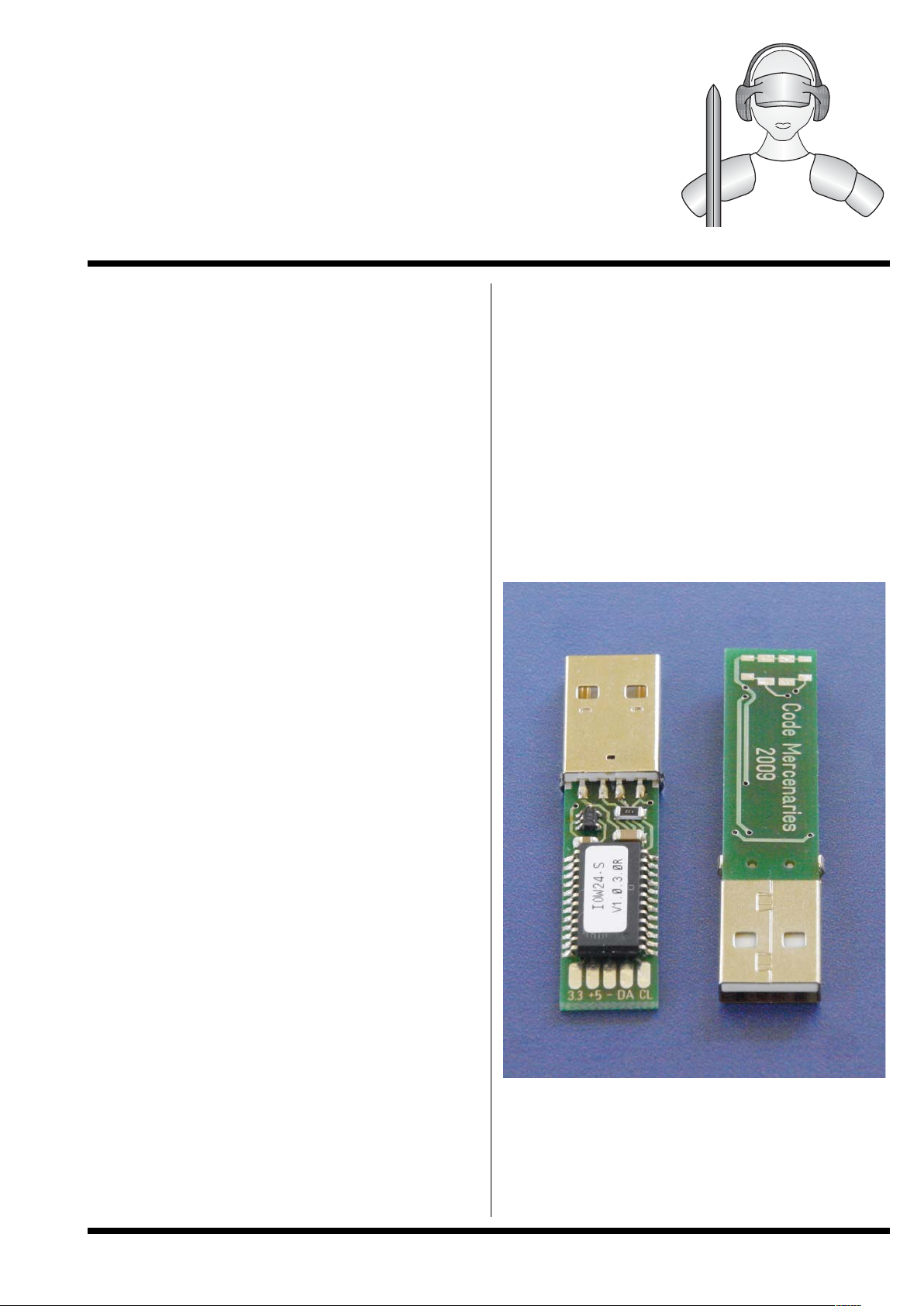
Dongle shown from both sides.
V1.0.0 September 8th 2009
USB to I2C Dongle
based on IO-Warrior24
Page 2

Code Mercenaries
2
IIIIOO
OO
WW
WW
22
22
44
44----
DD
DD
GG
GG
3.1 Compatibility with 3.3 V slaves
If a 3.3V slave is to be connected the internal pull
up resistors of the IOW24 should be switched off
by software on enabling the I2C function.
This requires external pull up resistors which may
be added either on the slave side or soldered to the
lower side of the dongle PCB. It is recommended
to add protection diodes so the slave does not see
5V on the signal lines before the I2C function of
the IO-Warrior24 is initialized.
There are landing pads for four components on the
lower side of the dongle PCB, the outer ones are
intended for pull up resistors, the inner ones for
protection diodes. The pads facing the end of the
board connect to 3.3 V.
Protection diodes must connect to 3.3 V with their
cathodes. MELF packages are not recommended
since they are too thick to fit in the dongle case
4. Software/Programming support
The IO-Warrior SDK is used with the dongle. The
SDK, additional software, and the data sheet for
the IO-Warrior is available on our website.
5. FCC / CE
The IOW24-DG is sold as kit. As such it can not be
FCC or CE approved.
Code Mercenaries has excerted greatest care in
designing this module to minimize RF emission
and assure stable operation. Though the use of
proper cable materials and correct integration into
a device is crucial to assure product safety and
interference free operation.
The integrator who assembles the module into a
device has to take care for appropriate testing and
safety measures.
6. Ordering information
The standard packaging for IOW24-DG is a blister
pack containing the parts for one unit.
The order code is:
IOW24-DG
Legal Stuff
This document is ©1999-2009 by Code
Mercenaries.
The information contained herein is subject to
change without notice. Code Mercenaries makes
no claims as to the completeness or correctness of
the information contained in this document.
Code Mercenaries assumes no responsibility for
the use of any circuitry other than circuitry
embodied in a Code Mercenaries product. Nor
does it convey or imply any license under patent or
other rights.
Code Mercenaries products may not be used in any
medical apparatus or other technical products that
are critical for the functioning of lifesaving or
supporting systems. We define these systems as
such that in the case of failure may lead to the
death or injury of a person. Incorporation in such a
system requires the explicit written permission of
the president of Code Mercenaries.
Trademarks used in this document are properties of
their respective owners.
Code Mercenaries
Hard- und Software GmbH
Karl-Marx-Str. 147a
12529 Schönefeld OT Grossziethen
Germany
Tel: x49-3379-20509-20
Fax: x49-3379-20509-30
Mail: support@codemercs.com
Web: www.codemercs.com
HRB 9868 CB
Geschäftsführer: Guido Körber, Christian Lucht
V1.0.0 September 8th 2009
Page 3
Code Mercenaries
1
IIIIOO
OO----
WW
WW
aa
aarrrrrrrriiii
oo
oorrrr
1.0 Features
• USB interface
• USB V1.1/2.0 compliant low speed device
• USB HID 1.1 compliant
• 32 general purpose I/O pins on IOW40
16 general purpose I/O pins on IOW24
• Supports IIC compatible devices
• Supports HD44780 compatible display modules
and several graphic display modules
• Supports SPI slave devices up to 2MBit/sec
(IOW24)
• Supports receiving RC5 IR remote control data
(IOW24)
• Drives LED matrix up to 8x32 with few
external shift registers
• Supports 8x8 or 16x8 switch or key matrix
(IOW40)
• Two 24 bit capture timers with 4sec resolution
(IOW24)
• Easy to use starter kit
• Software support for Mac, Linux, and Windows
• No USB knowledge necessary to use
• Single +5V power supply
• Available SSOP48 package and DIL40 module
(replacing PDIP40 package), or DIL24 and
SOIC24.
1.1 Variants
IO-Warrior is available in several variants. The
IOW24PowerVampire and the IO-Warrior56 are
covered by separate data sheets.
Custom modifications are possible.
IO-Warrior24
• 16 general purpose I/O pins, typ. 125Hz read
• IIC master, typ. 750 bytes/sec throughput
• Alphanumeric and graphic display support
• RC5 IR remote control receiver
• Hardware SPI master interface up to 2Mbit/sec
bitrate, typ. 750 bytes/sec throughput
• LED matrix with up to 8x32 LEDs with the
support of external register/drivers
• Two 24 bit capture timers with 4sec resolution
• Minimal external component count
• Identifies as either low power (100mA) or high
power (500mA) bus powered device. Pin
selectable
• Easy to use starter kit for immediate access
• DIL24 or SOIC24 package
IO-Warrior40
• 32 general purpose I/O pins, typ. 125Hz read
• IIC master, typ. 750 bytes/sec throughput
• Alphanumeric and graphic display support
• LED matrix with up to 8x32 LEDs with the
support of external register/drivers
• 8x8 or 16x8 switch or key matrix
• Minimal external component count
• Identifies as either low power (100mA) or high
power (500mA) bus powered device. Pin
selectable
• Easy to use starter kit for immediate access.
• SSOP48 package or DIL40 module (replacing
PDIP40 package)
1.2 Custom variants
Custom adaptions are available on request. If
necessary complex functions can be added to the
standard chips to directly control specific circuits.
2.0 Functional overview
IO-Warrior offers a simple access to the USB.
Many projects that formerly used the parallel port
or some other kind of direct I/O interface today
face the problem that getting simple things to work
on the USB is quite complex.
With a serial or parallel port you needed only a
simple circuit to control an external relay or read a
single switch. With USB you need a
microcontroller that handles all the protocol work
to do the same thing. Several standard commands
need to be supported to get a device accepted as a
USB device, let alone implementing any real
function.
IO-Warrior brings simplicity to the USB. The
protocol is encapsulated in the IO-Warrior Chip.
You only have to care about the 16 or 32 I/O pins
and have to write only a few simple lines of code
to access them.
IO-Warrior also supports a range of industrial
standard interfaces to simplify interfacing to
certain chips or modules. These interfaces are
handled internally in IO-Warrior removing the
bandwith wasting controlling of individual pins.
V 1.1.0, December 2nd 2013, for chip revision V1.0.3.0 and up
Generic universal I/O Controller
for USB
Page 4

Code Mercenaries
2
IIIIOO
OO----
WW
WW
aa
aarrrrrrrriiii
oo
oorrrr
Content
1.0 Features 1
1.1 Variants 1
1.2 Custom variants 1
2.0 Functional overview 1
2.1 Product selection matrix 3
3.0 Pin Configurations 5
4.0 Pin Descriptions IO-Warrior40 8
4.1 Pin Descriptions IO-Warrior24 8
4.2 Pin descriptions 9
4.3 Special mode pin functions 9
4.3.1 IIC Mode pins 10
4.3.2 LCD Mode pins 10
4.3.3 SPI Mode Pins (IOW24 only) 10
4.3.4 RC5 Mode Pins (IOW24 only) 10
4.3.5 LED Matrix Mode Pins 11
4.3.6 Switch Matrix Mode Pins (IOW40 only) 11
4.3.7 Capture Timer Mode Pins (IOW24 only) 11
5.0 Device Operation 12
5.1 Accessing IO-Warrior 12
5.2 IO-Warrior communication 12
5.3 IO-Warrior input behaviour 12
5.5 IO-Warrior output behaviour 12
5.6 Using pins as inputs or outputs 12
5.7 Power supply 13
5.8 Suspend 13
5.9 Remote Wakeup 13
5.10 Special mode I/O 14
5.10.1 IIC Special mode function 14
5.10.2 LCD Special mode function 16
5.10.3 SPI Special mode function (IOW24 only) 17
5.10.4 Getting current pin status 18
5.10.5 Receiving RC5 IR codes (IOW24 only) 18
5.10.6 Driving LED matrix 18
5.10.7 Switch Matrix Mode (IOW40 only) 19
5.10.8 Capture Timers (IOW24 V1.0.3.0 only) 20
7.1 Packaging info 24
7.2 USB VendorID and ProductID 24
7.3 Serial numbers 24
7.4 Currently shipping versions 24
8.2 Warning about USB cables 27
8.3 Jumpers on the IOW40 Starter Kit 27
8.3.1 Jumpers on the IOW24 Starter Kit 27
8.4 Adding custom circuits 27
8.5 Example circuits 27
8.5.1 Drivers 27
8.5.2 Isolating inputs 28
8.5.3 Protecting inputs and outputs 28
8.5.4 Using the LCD function 28
9.0 Package Dimensions 30
10.0 ESD Considerations 32
10.1 EMC Considerations 32
11.0 Revision History 33
12.0 Legal Stuff 34
V 1.1.0, December 2nd 2013, for chip revision V1.0.3.0 and up
Page 5
Code Mercenaries
3
IIIIOO
OO----
WW
WW
aa
aarrrrrrrriiii
oo
oorrrr
2.1 Product selection matrix
2.2 Starter Kits
With the IO-Warrior Starter Kits you can make your first steps with IO-Warrior40 or IO-Warrior24
easily. A couple elements on the kit allow first experiments with inputs and outputs, the bread board area
provides space to test your individual circuit. There are separate starter kits for IOW40 and IOW24.
The starter kits are sold unassembled. A couple minutes soldering will provide you with a working unit.
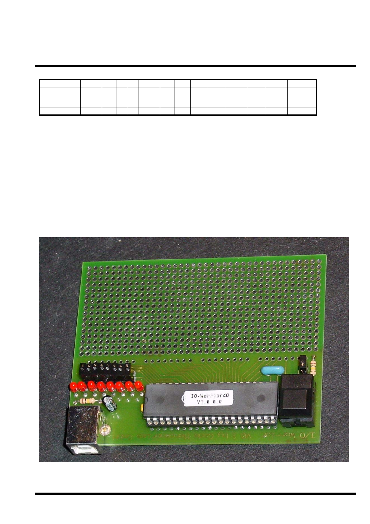
2.2.1The IO-Warrior40 Starter Kit
The IOW40KIT for IO-Warrior40 provides eight LEDs and a button that can be used for first
experiements. The starter kit is sold unassembled.
Assembled the starter kit for IO-Warrior40 looks similar to this:
Actual components supplied with the kit may vary from those shown here.
Type
IO-Warrior40
IO-Warrior24
I/O Pins
LCD
32
16
IO-Warrior24PV
IO-Warrior56
12
50
IIC SPI
RC5 IR Keys
LEDs Timer
DIL40 SSOP48
DIL24 SOIC24
Starter Kit
V 1.1.0, December 2nd 2013, for chip revision V1.0.3.0 and up
Page 6
Code Mercenaries
4
IIIIOO
OO----
WW
WW
aa
aarrrrrrrriiii
oo
oorrrr
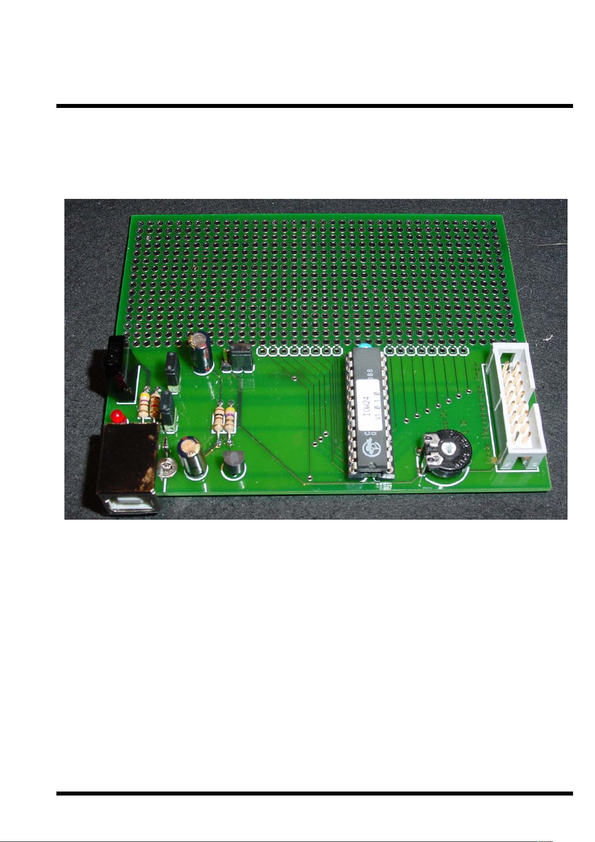
2.2.2 The IO-Warrior24 Starter Kit
The IOW24KIT for IO-Warrior24 provides a LED, an IR receiver, and the circuit and connector to
directly connect a LCD module.
The starter kit is sold unassembled.
Assembled the starter kit for IO-Warrior24 looks similar to this:
Actual components supplied with the kit may vary from those shown here.
V 1.1.0, December 2nd 2013, for chip revision V1.0.3.0 and up
Page 7
Code Mercenaries
5
IIIIOO
OO----
WW
WW
aa
aarrrrrrrriiii
oo
oorrrr
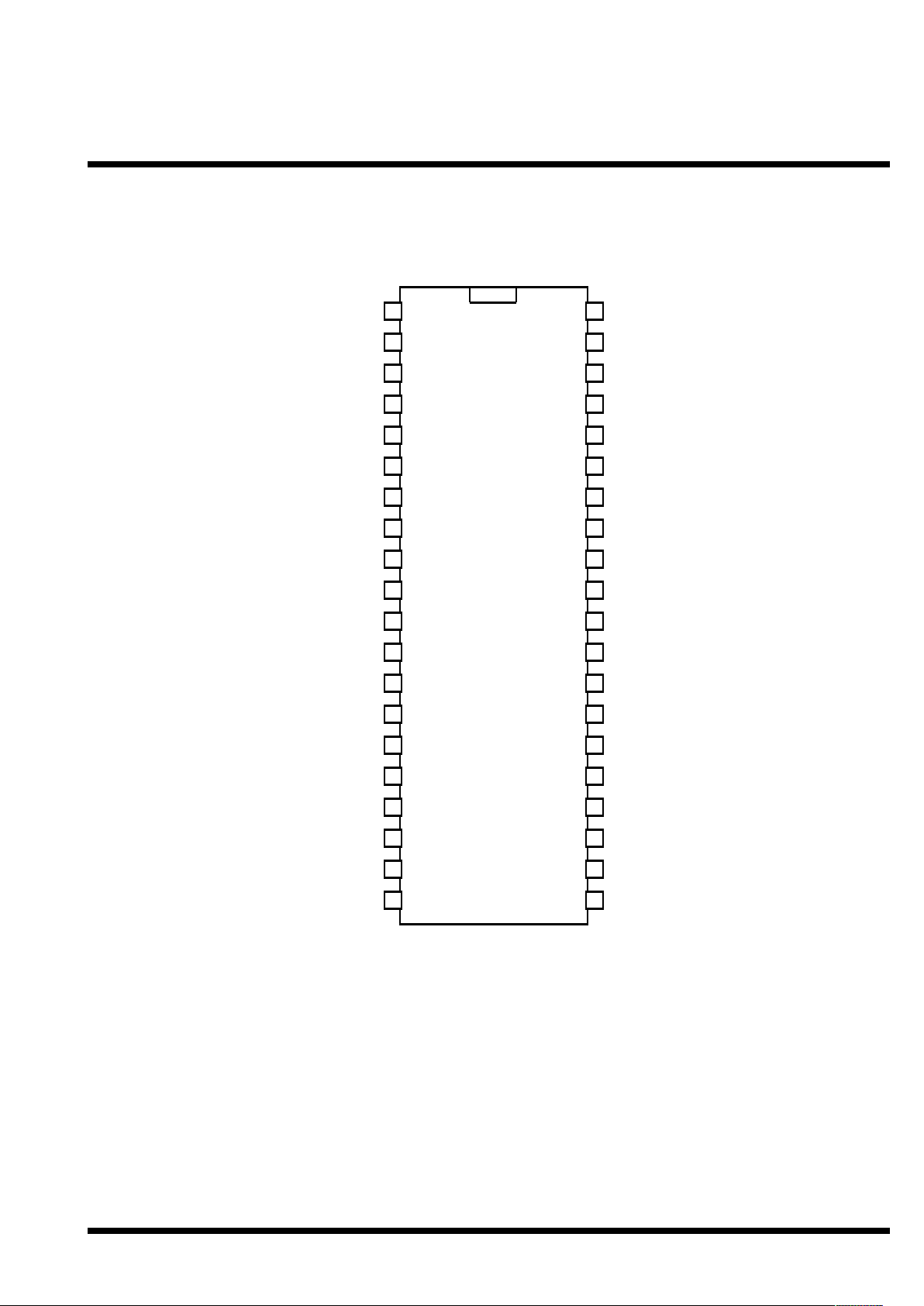
3.0 Pin Configurations
IO-Warrior40-MOD
DIL40 Module
All drawings: TOP VIEW!
1
2
3
4
5
6
7
8
9
10
11
12
13
14
15
16
17
18
19
20
40
39
38
37
36
35
34
33
32
31
30
29
28
27
26
25
24
23
22
21
DDDD++
++
DDDD--
--
PPPP3333....7777////YYYY77
77
PPPP3333....6666////YYYY66
66
PPPP3333....5555////YYYY5
5
55
PPPP3333....4444////YYYY44
44
PPPP3333....2222////YYYY22
22
PPPP3333....1111////YYYY11
11
PPPP3333....00
00////YYYY0000
PPPP2222....7777////XXXX77
77
PPPP2222....6666////XXXX66
66
PPPP2222....5555////XXXX55
55
PP
P
P2222....4444////XXXX4444
PPPP2222....3333////XXXX33
33
PPPP2222....2222////XXXX22
22
PPPP2222....1111//
//
XXXX11
11
PPPP2222....0000////XXXX00
00
LLLLCCCCDDDD----DDDDBBBB7777////PPPP1111....7777////XXXX111155
55
P
PPP1111....6666////LLLLCCCCDDDD----DDDDBBBB6666////XXXX111144
44
LLLLCCCCDDDD----DDDDBBBB5555////PPPP11
11....5555////XXXX11113333
PPPP1111....4444////LLLLCCCCDDDD----DDDDBBBB4444////XXXX111122
22
LLLLCCCCDD
D
D----DDDDBBBB3333////PPPP1111....3333////XXXX11111111
PPPP1111....2222////LLLLCCCCDDDD----DDDDBBBB2222////XXXX111100
00
LLLLCCCCDDDD----DDDDBBBB1111////PPPP1111....1111////XXXX99
99
PPPP1111....0000////LLLLC
CCCDDDD----DDDDBBBB0000////XXXX88
88
IIIIIIIICCCC----SSSSDDDDAAAA////PPPP0000....77
77
PPPP0000....6666//
//
IIIIIIIICCCC----SSSSCCCCLL
LL
LLLLCCCCDDDD----EEEE////PPPP0000....55
55
PPPP0000....4444////LLLLCCCCDDDD--
-
-RRRR////WWWW
LLLLCCCCDDDD----RRRRSSSS////PPPP0000....33
33
PPPP0000....2222////LLLLCCCCDDDD----////OO
OO
nn
nn
PPPP0000....11
11
PPPP0000....00
00
PPPPuuuullllllllTTTTooooGGGGNNNNDD
DD
GGGGNNNNDD
DD
XXXXIIIInn
nn
XXXXOO
OO
uuuutt
tt
GGGGNNNNDD
DD
VVVVcccccc
cc
PPPP3333....3333////YYYY33
33
V 1.1.0, December 2nd 2013, for chip revision V1.0.3.0 and up
Page 8
Code Mercenaries
6
IIIIOO
OO----
WW
WW
aa
aarrrrrrrriiii
oo
oorrrr
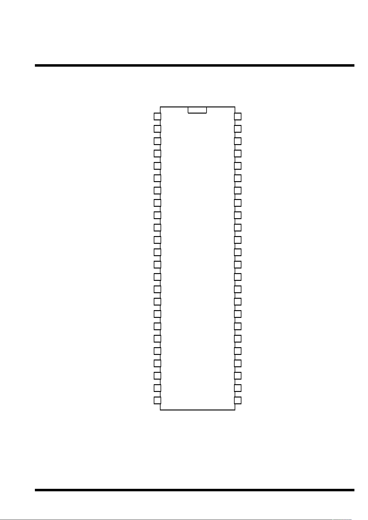
IO-Warrior 40-S
SSOP48
All drawings: TOP VIEW!
1
2
3
4
5
6
7
8
9
10
11
12
13
14
15
16
17
18
19
20
40
39
38
37
36
35
34
33
32
31
30
29
28
27
26
2524
23
22
21
DDDD++
++
DDDD--
--
PPPP3333....7777////XXXX77
77
PPPP3333....6666////YYYY66
66
PPPP3333....5555////XX
X
X5555
PPPP3333....4444////YYYY44
44
PPPP3333....2222////YYYY22
22
PPPP3333....1111////XXXX11
11
PPPP3333..
..
0000YYYY00
00
NNNNCC
CC
NNNNCC
CC
NNNNCC
CC
NNNNCC
CC
NNNNCC
CC
NNNNCC
CC
NNNNCC
CC
NNNNCC
CC
LLLLCCCCDDDD----DDDDBBBB7
777////PPPP1111....7777////XXXX111155
55
PPPP1111....6666////LLLLCCCCDDDD----DDDDBBBB6666////XXXX111144
44
LLLLCCCCDDDD----DDDDBBBB5555////PPPP1111....5555////XXXX111133
33
PPPP1111....4444////LLLLCCCCDDDD--
-
-DDDDBBBB4444////XXXX11112222
LLLLCCCCDDDD----DDDDBBBB3333////PPPP1111....3333////XXXX111111
11
PPPP11
11
....2222////LLLLCCCCDDDD----DDDDBBBB2222////XXXX111100
00
LLLLCCCCDDDD----DDDDBBBB1111////PPPP1111....1
111////XXXX99
99
PPPP1111....0000////LLLLCCCCDDDD----DDDDBBBB0000////XXXX88
88
IIIIIIIICCCC----SSSSDDDDAA
AA
////PPPP0000....77
77
PPPP0000....6666////IIIIIIIICCCC----SSSSCCCCLL
LL
LLLLCCCCDDDD----EEEE////PPPP0000..
.
.5555
PPPP0000....4444////LLLLCCCCDDDD----RRRR////WW
WW
LLLLCCCCDDDD----RRRRSSSS////PPPP0000....33
33
PP
PP
0000....2222////LLLLCCCCDDDD----////OOOOnn
nn
PPPP0000....11
11
PPPP0000....00
00
PPPPuuuullllllllTTTTooooGG
G
GNNNNDDDD
GGGGNNNNDD
DD
XXXXIIIInn
nn
XXXXOOOOuuuutt
tt
GGGGNNNNDD
DD
VVVVcccccc
cc
41
42
43
44
45
46
47
48
PPPP3333....3333////XXXX33
33
PPPP2222....7777////XXXX77
77
PPPP2222....6666////XXXX66
66
PPPP2222....55
5
5////XXXX5555
PPPP2222....4444////XXXX44
44
PPPP2222....3333////XXXX33
33
PPPP2222....2222////XXXX22
22
PP
PP
2222....0000////XXXX00
00
PPPP2222....1111////XXXX11
11
V 1.1.0, December 2nd 2013, for chip revision V1.0.3.0 and up
Page 9
Code Mercenaries
7
IIIIOO
OO----
WW
WW
aa
aarrrrrrrriiii
oo
oorrrr
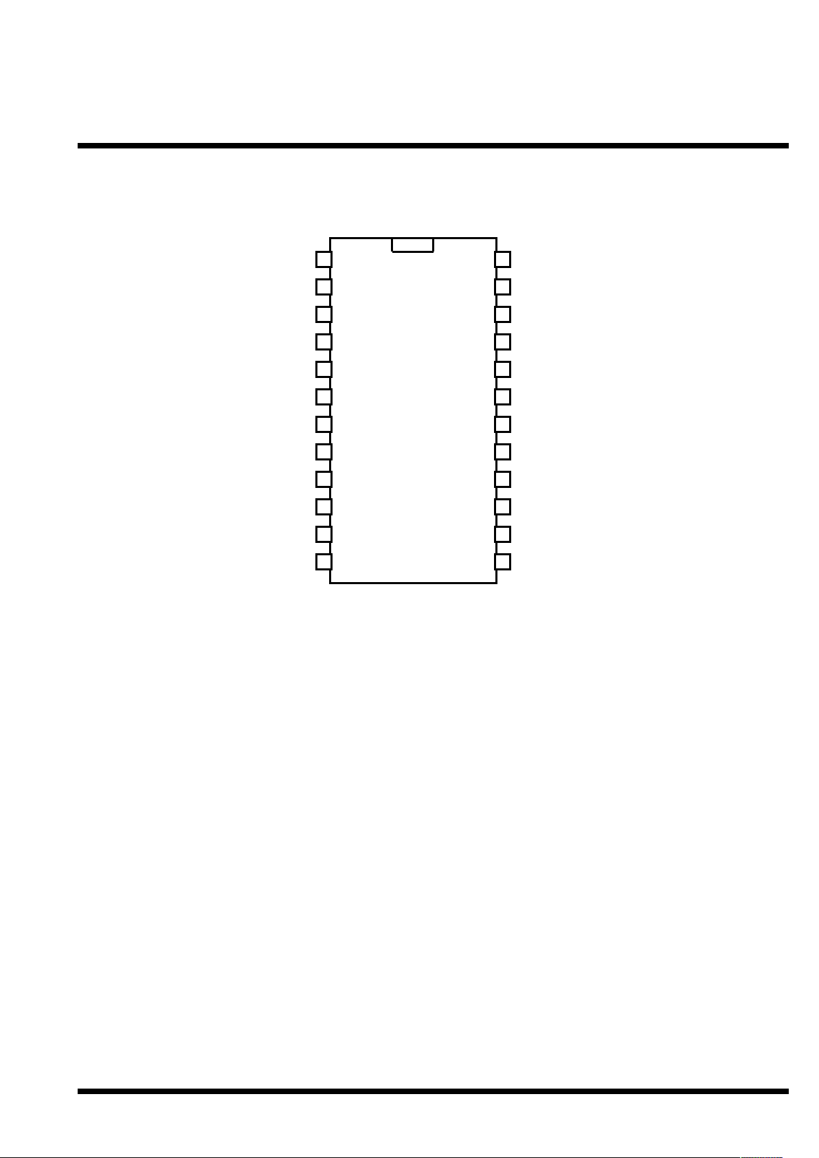
IO-Warrior 24-P/-S
DIL24 / SOIC24
All drawings: TOP VIEW!
1
2
3
4
5
6
7
8
9
10
11
12 13
14
15
16
17
18
19
20
PPPP0000....0000////RRRRxxxxDDDD////CCCCAAAAPPPPAA
AA
IIIIIIIICCCC----SSSSCCCCLLLL////PPPP0000....11
11
////CCCCAAAAPPPPBB
BB
IIIIIIIICCCC----SSSSDDDDAAAA////PPPP0000....22
22
PPPP0000....6666////SSSSPPPPIIII--
--
MMMMIIIISSSSOOOO////LLLLCCCCDDDD----RRRR////WW
WW
SSSSPPPPIIII----DDDDRRRRDDDDYYYY////PPPP0000....33
33
LL
L
LCCCCDDDD----DDDDBBBB0000////PPPP1111....0000
LLLLCCCCDDDD----DDDDBBBB4444////PPPP1111....44
44
PPPP11
11....1111////LLLLCCCCDDDD----DDDDBBBB1111
LLLLCCCCDDDD----DDDDBBBB2222////PPPP1111....22
22
PPPP1111....3
333////LLLLCCCCDDDD----DDDDBBBB33
33
GGGGNNNNDD
DD
DDDD++
++
PPPPuuuullllllllTTTTooooGGGGNNNNDD
DD
DDDD--
--
VV
VV
rrrreeeegg
gg
VVVVcccccc
cc
PPPPoooowwwweeeerr
rr
NNNNCC
CC
PPPP0000....5555////SSSSPPPPIIII----MMMMOOOOSSSSII
I
I////LLLLCCCCDDDD----RRRRSSSS
PPPP0000....4444////SSSSPPPPIIII----SSSSSSSS////LLLLCCCCDDDD----////OOOOn
n
nn
21
22
23
24
LLLLCCCCDDDD----DDDDBBBB6666////PPPP1111....66
66
PPPP1111....7777////LLLLCCCCDDDD----DDDDBBBB77
77
PP
P
P0000....7777////SSSSPPPPIIII----SSSSCCCCKKKK////LLLLCCCCDDDD----EEEE
PPPP1111....5555////LLLLCCCCDDDD-
---DDDDBBBB55
55
V 1.1.0, December 2nd 2013, for chip revision V1.0.3.0 and up
Page 10
Code Mercenaries
8
IIIIOO
OO----
WW
WW
aa
aarrrrrrrriiii
oo
oorrrr
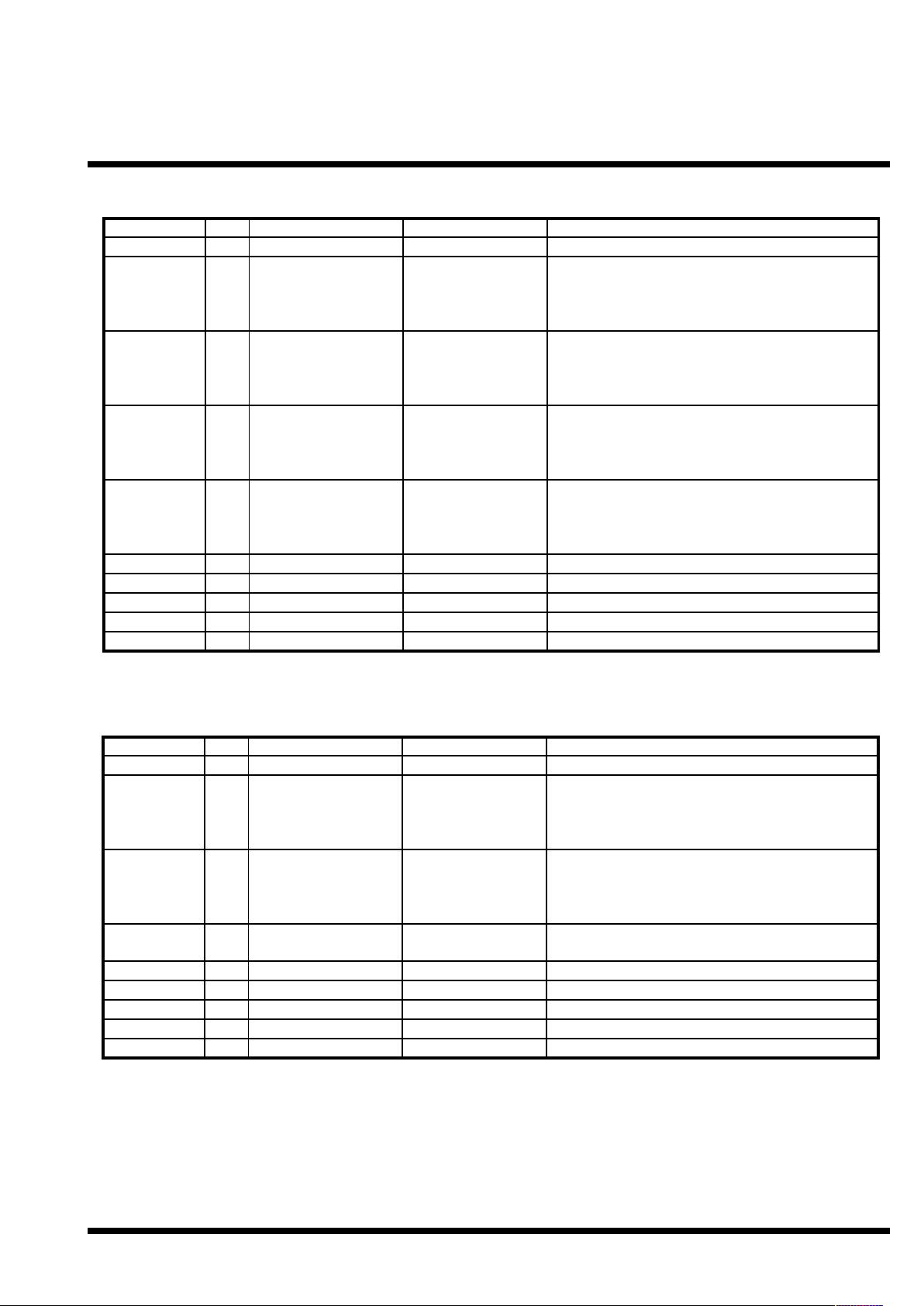
4.0 Pin Descriptions IO-Warrior40
4.1 Pin Descriptions IO-Warrior24
Name
I/O
Type
Pins (DIL40)
Description
D+, D-
P0.0, P0.1,
P0.2, P0.3,
P0.4, P0.5,
P0.6, P0.7
I/O
I/O
special
I/O open drain, internal
pullup
1, 2
23, 18, 24, 17, 25, 16,
26, 15
USB differential data lines
First I/O Port. P0.0 is used at power on to select low
or high power mode
P1.0, P1.1,
P1.2, P1.3,
P1.4, P1.5,
P1.6, P1.7
P2.0, P2.1,
P2.2, P2.3,
P2.4, P2.5,
P2.6, P2.7
P3.0, P3.1,
P3.2, P3.3,
P3.4, P3.5,
P3.6, P3.7
PullToGND
I/O
I/O
I/O open drain, internal
pullup
I/O open drain, internal
pullup
I/OII/O open drain, internal
pullup
27, 14, 28, 13, 29, 12,
30, 11
31, 10, 32, 9, 33, 8,
34, 7
Second I/O Port
Third I/O Port.
35, 6, 36, 5, 37, 4, 38,
3
19
Fourth I/O Port. P3.7 must be pulled high with a
100k resistor for proper operation of the chip.
Strong drive outputs, capable of driving LEDs
direct.
Used during manufacturing, connect to GND
GND
Vcc
XOut
XIn
Power supply
Power supply
OI20, 39
40
Ground
Supply voltage
2221On chip oscillator output
On chip oscillator input
Name
I/O
Type
Pins
Description
D+, D-
P0.0, P0.1,
P0.2, P0.3,
P0.4, P0.5,
P0.6, P0.7
I/O
I/O
special
I/O open drain, internal
pullup
16, 15
1, 2, 3, 4, 24, 23, 22,
21
USB differential data lines
First I/O Port.
P1.0, P1.1,
P1.2, P1.3,
P1.4, P1.5,
P1.6, P1.7
Power
PullToGND
GND
I/OII/O open drain, internal
pullup
Input internal pull
down
I
Power supply
5, 20, 6, 19, 7, 18, 8,
17
12
Second I/O Port
Used to set high or low power mode
109Used during manufacturing, connect to GND
Ground
Vcc
VregNCO
Power supply
Regulated 3V out
-1411
Supply voltage
Power for D- pullup resistor
13
do not connect
V 1.1.0, December 2nd 2013, for chip revision V1.0.3.0 and up
Page 11

Code Mercenaries
9
IIIIOO
OO----
WW
WW
aa
aarrrrrrrriiii
oo
oorrrr
4.2 Pin descriptions
D+, D-
Differential data lines of USB. Connect these
signals direct to a USB cable. D- requires a pull up
resistor, see application circuit for details.
For a PCB layout make sure to run these two
signals next to each other. USB data is a
differential signal that produces best signal quality
and lowest RF emission if the two lines are close to
each other.
P0.0..P0.7
First I/O port of the chip. These pins correspond
with the lowest 8 bits of the input or output (bits
0..7).
On IOW40 P0.0 serves the double purpose of
determining the power mode of the chip. To set the
desired power mode P0.0 must be pulled high or
low using a 100k resistor (or less). IO-Warrior40
reads the status on this pin after a reset prior to
enabling the internal pull up resistor.
A high on P0.0 on reset sets the high power mode,
this means the IO-Warrior40 will report as a high
power, bus powered device drawing up to 500mA.
Pulling P0.0 low on reset sets the low power mode
specifying 100mA maximum power draw.
P1.0..P1.7
Second I/O Port. Corresponds to the bits 8..15.
P2.0..P2.7 (IOW40 only)
Third I/O Port. Corresponds to the bits 16..23.
P3.0..P3.7 (IOW40 only)
Fourth I/O Port. Corresponds to the bits 24..31.
P3.7 does need to be pulled high with a
100kresistor on power up. This is necessary for
proper function of the chip.
P3.0..P3.7 have sufficient current sinking
capability to directly drive LEDs.
Pull to GND
This pin is used during production of the IOWarrior chips, connect to GND.
XOut, XIn (IOW40 only)
Connection for external oscillator. A 6MHz
ceramic resonator should be connected here, no
additional components necessary.
Using a crystal results in unstable operation as the
oscillator is optimized for use with ceramic
resonators.
An external 6MHz clock may be connected to XIn,
XOut has to be left floating in this case.
GND
Power supply ground.
Vcc
Supply voltage.
A 100nF ceramic capacitor is required to be
connected directly to the power supply pins. The
two ground pins of IO-Warrior have to be
connected in the shortest possible way, no other
considerations may have any precedence over this.
Vreg (IOW24 only)
Regulated 3V output, to be used only for the
purpose of powering the USB D- pull up resistor.
Do not use this pin as a supply for any other circuit
than the pull up resistor.
Power (IOW24 only)
Input to set the power mode. The status of the pin
is checked only at power up and bus reset. Pulling
this pin to high sets high power mode, this means
the IO-Warrior24 will report as a high power, bus
powered device drawing up to 500mA. Pulling
Power low on reset sets the low power mode
specifying 100mA maximum power draw.
4.3 Special mode pin functions
IO-Warrior supports driving IIC compatible chips
and HD44780 compatible display modules and
some other display modules direct. IO-Warrior24
does also have a SPI interface. Handling IIC via
the normal generic I/O would be very slow as each
edge of data and clock would have to be
transmitted separately. At a rate of 125 such
transactions per second (which is about the
maximum IO-Warrior is allowed by USB
specifications) the maximum bit rate would be
around 30 bits/sec.
To make IIC and other devices usable IO-Warrior
implements the special mode functions. By
handling the IIC inside IO-Warrior the actual data
rate is increased to about 6000 bits/sec or 750
bytes/sec.
When any of the special mode functions is
activated a couple pins will no longer respond as
generic I/O pins but are under control of the
activated special mode function.
V 1.1.0, December 2nd 2013, for chip revision V1.0.3.0 and up
Page 12

Code Mercenaries
10
IIIIOO
OO----
WW
WW
aa
aarrrrrrrriiii
oo
oorrrr
4.3.1 IIC Mode pins
IO-Warrior can act as an IIC master with about
100kbit/sec data rate (actual throughput is about
750bytes/sec). Multi-Master mode is not supported
by IO-Warrior, it has to be the only master on the
IIC.
Since the IIC bus in IO-Warrior is software driven
it does not have as stable a clock timing as
hardware IIC masters have. Make sure that the
devices you drive with IO-Warrior don't have a
problem with some clock jitter.
The following pins get reassigned when the IIC
function is enabled:
These pins will no longer be affected by the data
sent via the normal port setting command. Both
pins have internal pull up resistors and can be
connected direct to IIC compatible chips.
On IOW24 simultaneous use of the IIC function
and capture timer B is not possible.
4.3.2 LCD Mode pins
IO-Warrior has support for controlling alphanumeric display modules based on or compatible
with HD44780 as well as some graphic displays.
Attention: IOW24 can use either LCD or SPI but
never both at the same time.
IOW40 can use either 16x8 key matrix mode or
LCD, never both at the same time.
LCD mode and LED matrix mode can not be used
at the same time on IOW24 and IOW40.
The following pins get reassigned when the LCD
function is enabled:
When the LCD function is enabled these pins will
no longer be affected by the normal port setting
command.
/On should be used to enable power supply to LCD
modules that have high current demand or
backlighting. The /On signal is low when the LCD
function is enabled, it does go high when IOWarrior enters suspend mode or when the LCD
function is disabled.
4.3.3 SPI Mode Pins (IOW24 only)
IO-Warrior24 supports a hardware SPI master
interface. This means it can talk to SPI slave
devices with a data clock speed of up to 2MHz.
Actual data throughput is significantly lower since
USB allows only 100 reports per second to be send
to low speed devices (actual system
implementations allow 125 reports per second)
The following pins get reassigned when the SPI
function is enabled:
When the SPI function is enabled these pins will
no longer be affected by the normal port setting
command.
SPI and LCD can not be used at the same time
since these functions share some pins.
4.3.4 RC5 Mode Pins (IOW24 only)
IO-Warrior24 supports receiving IR remote control
commands according to the RC5 code.
For this function it is necessary to connect an
appropriate IR receiver module like the Vishay
TSOP1736.
The following pins get reassigned when the RC5
function is enabled:
When the RC5 function is enabled these pins will
no longer be affected by the normal port setting
command.
RC5 mode can not be used at the same time as any
of the capture timers.
Function IOW24 IOW40
SCL
SDA
P0.1
P0.2
P0.6
P0.7
Function IOW24 IOW40
/On
RS
P0.4
P0.5
P0.2
P0.3
R/W
E
Data0
Data1
P0.6
P0.7
P0.4
P0.5
P1.0
P1.1
P1.0
P1.1
Data2
Data3
Data4
Data5
P1.2
P1.3
P1.2
P1.3
P1.4
P1.5
P1.4
P1.5
Data6
Data7
P1.6
P1.7
P1.6
P1.7
Function IOW24 IOW40
/DRDY
/SS
P0.3
P0.4
-
MOSI
MISO
SCK
P0.5
P0.6
-
-
P0.7 -
Function IOW24 IOW40
RxD P0.0 -
V 1.1.0, December 2nd 2013, for chip revision V1.0.3.0 and up
Page 13

Code Mercenaries
11
IIIIOO
OO----
WW
WW
aa
aarrrrrrrriiii
oo
oorrrr
4.3.5 LED Matrix Mode Pins
IO-Warrior supports driving a LED matrix with up
to 8x32 LEDs. The LED matrix mode can not be
used at the same time as the LCD mode. IOW40
can use either 16x8 key matrix mode or LED
matrix mode, never both at the same time.
When the LED Matrix function is enabled these
pins will no longer be affected by the normal port
setting command.
/OE is driven high when IO-Warrior enters the
suspend mode. The external driver should then
disable to stay within the USB power limits for
suspend mode.
For more details on how to control a LED matrix
please refer to the separate application note.
4.3.6 Switch Matrix Mode Pins (IOW40 only)
IO-Warrior40 supports scanning of a 8x8 or 16x8
matrix of keys or switches. When this function is
enabled P3.0..7 will turn off their internal pull up
resistors and will be used as the Y lines that are
periodically driven to Gnd voltage level. P2.0..7
will serve as the X0..7 matrix inputs, they will
keep their internal pull up resistors active so a
closed switch in the matrix will pull down the X
line when the corresponding Y line is driven low.
If the 16x8 mode is enabled P1.0..7 will be used as
additional X lines, serving as X8..15. The 16x8
matrix mode can be used only if the LCD and LED
matrix functions are not in use.
To allow more than two switches to be closed at
the same time and still be able to faultlessly detect
which of the matrix points are closed it is
necessary to insert a diode in series with every key
or switch in the matrix. The kathodes of the diodes
have to be connected to the Y lines (P3.0..7).
The following pins get reassigned when the key
mode is enabled:
When IO-Warrior40 enters the suspend mode the
X and Y lines will be pulled high by internal pull
up resistors. Closing a switch/key does not wake
the IO-Warrior.
4.3.7 Capture Timer Mode Pins (IOW24 only)
IO-Warrior24 has two capture timers that can
measure falling and rising edges with a resolution
of 4sec. When this function is turned on P0.0 and/
or P0.1 will be used for the timers and be no longer
available for standard I/O. P0.0 is shared between
the RC5 receiver and capture timer A. P0.1 is
shared between the IIC function and capture timer
B. The RC5 receiver and the capture timers can not
be used at the same time since they share internal
resources on the chip.
Function IOW24 IOW40
/OE
Strb
P1.0
P1.1
P1.0
P1.1
Clk
Data
P1.2
P1.3
P1.2
P1.3
Function IOW24 IOW40
X0
X1
-
-
P2.0
P2.1
X2
X3
X4
X5
-
-
P2.2
P2.3
-
-
P2.4
P2.5
X6
X7
X8
X9
-
-
P2.6
P2.7
-
-
P1.0
P1.1
X10
X11
X12
X13
-
-
P1.2
P1.3
-
-
P1.4
P1.5
X14
X15
Y0
Y1
-
-
P1.6
P1.7
-
-
P3.0
P3.1
Y2
Y3
Y4
Y5
-
-
P3.2
P3.3
-
-
P3.4
P3.5
Y6
Y7
-
-
P3.7
P3.7
Function IOW24 IOW40
Capture A
Capture B
P0.0
P0.1
-
-
V 1.1.0, December 2nd 2013, for chip revision V1.0.3.0 and up
Page 14

Code Mercenaries
12
IIIIOO
OO----
WW
WW
aa
aarrrrrrrriiii
oo
oorrrr
5.0 Device Operation
Due to the fact that all current operating systems
offer an especially easy access to devices in the
HID class, IO-Warrior was designed as a generic
HID device. While this does not exactly fit the
device it makes using it a lot easier.
By identifying as a generic HID class device IOWarrior avoids being controlled by any of the
higher level system drivers, which makes it
possible to access IO-Warrior from application
level.
5.1 Accessing IO-Warrior
A common misconception with people new to the
USB is that they think they can "talk to the USB
port". The truth is that you do that as likely as you
are going to directly talk to your Ethernet port or
PCI bus.
Communication on the USB is always with a
specific device attached to the USB. The USB
itself is only the medium through which you
communicate.
To get access to a certain device you have to look
for the VendorID and ProductID of that device.
The specific mechanisms for doing so depend on
the individual operating system.
For details refer to our sample code.
5.2 IO-Warrior communication
IO-Warrior has three USB endpoints. Endpoints
are like virtual communication ports into or out of
the device.
An endpoint can be assigned to an interface.
Interfaces are like virtual devices or subsystems
within a device. IO-Warrior uses interface 0 to talk
to the pins directly and interface 1 to talk to the
special mode functions.
Endpoint 0 is a standard endpoint that is present on
all USB devices. It does use the control transfer
mode and is used by the system to get information
about the device and to configure the device.
Endpoint zero can also be used to send data to the
devices functions. IO-Warrior is using endpoint
zero for the output data and to send commands to
the special mode functions.
A SetReport request sending a four byte output
report (two bytes for IOW24) to interface 0 sets the
port pins. SetReport requests to interface 1 with a
length of 8 bytes are used to control the special
mode functions.
For input data IO-Warrior is using endpoint 1 as an
interrupt-in endpoint. Interrupt in this case is a bit
misleading. For USB interrupt means that data is
sent when there is new data available, the host
computer is periodically asking the device for new
data, the device itself can not initiate the data
transfer. IO-Warrior sends a new report any time it
detects a change to the input pin status.
Reactions to commands to the special mode
functions are sent via endpoint 2, also in interrupt
transfer mode.
5.3 IO-Warrior input behaviour
IO-Warrior scans the status of all pins once every
millisecond. If it detects a change from the last
status a new report via endpoint 1 is issued. Pins
which are currently used by a special mode
function are not checked.
Some care must be taken to not input signals with
frequencies too high for IO-Warrior to handle
properly.
Should the signal return to its former status before
the new report is send off this report gets
overwritten by the next one indicating the original
status. So it will look like nothing happened.
Due to the protocol specifics of USB it is only
possible to send one report every 10msec. Though
most OSes implement their USB in a way that
results in one report every 8msec.
5.5 IO-Warrior output behaviour
Upon receiving a SetReport request IO-Warrior
writes the new data to the output pins in groups of
eight pins each. Pins 0.0 to 0.7 get the new data
first, then 1.0 to 1.7, 2.0 to 2.7, and last 3.0 to 3.7.
The time between the individual output chunks is
about 1.5sec.
5.6 Using pins as inputs or outputs
All I/O pins on IO-Warrior can be used as input or
output pins.
Basically all pins act as inputs all of the time.
When receiving an input report from IO-Warrior
you always get the current status on the pins.
Writing a 0 as output value to any pin causes it to
drive the pin low with an open drain driver.
Usually this will result in this pin being read as a
zero input as well, unless so much current has to be
drained by the pin that the voltage at it gets above
the threshold level (you will see this when driving
the LEDs on the starter kit).
Writing a 1 to a pin causes the open drain driver to
be turned off. The pin will be pulled high by an
internal pull up resistor. Now the pin acts either as
an output with a high level, or can be used as an
input.
V 1.1.0, December 2nd 2013, for chip revision V1.0.3.0 and up
Page 15

Code Mercenaries
13
IIIIOO
OO----
WW
WW
aa
aarrrrrrrriiii
oo
oorrrr
5.7 Power supply
USB does allow a device to be "Bus Powered".
This means the device does get its power off the
USB port. To avoid overloading on the USB ports
devices need to advertise their power requirements.
There are two power classes for devices: Low
power and high power. Low power devices may
draw up to 100mA off the USB, high power
devices up to 500mA.
Likewise there are high power and low power
ports. Usually high power ports are those on the
motherboard and on hubs with external power
supply or hubs in a monitor. Low power ports are
typically on hubs that get their power off the USB,
like hubs in keyboards.
If the system decides that there is not sufficient
power to supply a high power decive that device
does not get enabled.
IO-Warrior can operate either as a high power or
low power device. Pulling the P0.0 pin on IOW40
or the Power pin on IOW24 high or low at reset
sets the desired power rating.
This allows to configure IO-Warrior optimally for
supporting external circuits.
5.8 Suspend
All devices on the USB port need to support the
suspended state. When the host computer stops to
periodically access the USB, like when it goes to
sleep, all devices need to enter the suspended state
and drop their power draw to less than 500A for
low power devices or less than 2.5mA for high
power devices.
When entering suspended state IO-Warrior pulls
all pins high. Care must be taken in designing
external circuits so that they will draw no more
than the allowed suspend power rating while all
pins of IO-Warrior are high.
5.9 Remote Wakeup
IO-Warrior chips support the remote wakeup
feature. They are able to wake the host computer
from sleep state if the host operating system has
enabled this feature.
Remote wakeup is initiated by IO-Warrior if any
pin is pulled low while the chip is in suspended
state.
V 1.1.0, December 2nd 2013, for chip revision V1.0.3.0 and up
Page 16

Code Mercenaries
14
IIIIOO
OO----
WW
WW
aa
aarrrrrrrriiii
oo
oorrrr
5.10 Special mode I/O
To enable IO-Warrior to talk to devices that have
more complex demands we have added the special
mode functions. When any of these functions is
enabled a couple pins of IO-Warrior turn into
special function pins.
Talking to the special mode functions is handeled
via the USB interface 1, which is also configured
as generic HID compliant.
Commands to the functions are sent via endpoint 0
as SetReport requests to interface 1. Replies from
the functions are returned as interrupt in reports via
endpoint 2.
To talk to these functions and to handle different
requests to them ReportIDs are used which enable
multiple functions to use the same endpoint. All
reports to and from special mode interfaces are
always eight bytes long, including the ReportID.
The following chapters describe the individual
special mode functions.
5.10.1 IIC Special mode function
The IIC function is enabled and disabled by
sending a report with the following structure with
ReportID=1 to interface 1:
enable=$01 enables the IIC function, $00 disables
it. Other values are reserved for future use.
Upon enabling IIC the SDA and SCL pins are
pulled high and are no longer under control of
SetReport requests to interface 0. Disabling IIC
does return the pins under control of interface 0
and pulls them high initially.
flags is used to deactivate the internal pull up
resistors for SDA and SCL (only on IOW24) and/
or select the use of the Sensirion protocol:
7 - Disable Pull Ups (1 = disable) - IOW24 only
6 - Use Sensibus Protocol (1 = enable)
5 - unused, write zero
4 - unused, write zero
3 - unused, write zero
2 - unused, write zero
1 - unused, write zero
0 - unused, write zero
Bit 7 - "Disable Pull Up" is available only on
IOW24. When this bit is set the internal pull up
resistors of the IIC pins are disabled. The status of
the pull up resistors can not be changed while the
IIC function is active. Disabling and again
enabling the IIC function is necessary to change
the status of the pull-up resistors.
Bit 6 - "Use Sensibus Protocol" selects the use of
the Sensirion protocol variant if set. The only
difference is that the start and stop conditions are
handeled according to the Sensirion protocol and a
handshake on read is added. The Sensibus protocol
can be activated and deactivated while the IIC
functions is active by sending another enable
command with this bit set differently.
The timeout byte sets the maximum time IOW
waits for SCL to be released by the slave when
clock stretching handshake is used. Time is
timeout x 500sec, writing a zero sets timeout to
256x500sec.
If the timeout expires due to the slave pulling down
SCL too long, IO-Warrior will return an error, just
like when the slave generates no Ack signal.
A write request to the IIC is send with ReportID=2
and has the following format:
flags contains the following bits:
7 - Generate Start
6 - Generate Stop
5 - unused, write zero
4 - unused, write zero
3 - unused, write zero
2 - data count MSB
1 - data count
0 - data count LSB
If bit 7 - "Generate Start" is set a start signal (SDA
falling edge while SCL is high) is generated on the
IIC prior to sending out the first data byte.
Bit 6 - "Generate Stop" causes a stop signal (SDA
goes high while SCL is high) to be generated after
sending the last valid data byte of this report.
"data count" gives the number of valid data bytes
in the report. The number may range from zero to
six, higher values cause the report to be ignored.
To do write transactions that are longer than six
bytes, send the first report with just the "Generate
Start" bit set, then send additional reports with
neither bit 6 or 7 set until the report with the last
bytes is send which has the "Generate Stop" bit set.
ReportID
$01 out
12
enable flags
34
timeout $00
56
$00 $007$00
ReportID
$02 out
12
flags data
34
data data
56
data data7data
V 1.1.0, December 2nd 2013, for chip revision V1.0.3.0 and up
Page 17

Code Mercenaries
15
IIIIOO
OO----
WW
WW
aa
aarrrrrrrriiii
oo
oorrrr
Any write transactions are acknowledged by a
report via interrupt-in endpoint 2:
flags contains the following bits:
7 - Error bit, 1=error
6 - unused, zero
5 - unused, zero
4 - unused, zero
3 - unused, zero
2 - data count MSB
1 - data count
0 - data count LSB
"data count" indicates the last byte that was
successfully transfered and acknowledged by the
slave (if any). An error is indicated when the slave
does not acknowledge a transfer.
Reading data off the IIC is initiated with a
ReportID=3. The initiating report has the following
format:
"command" holds the command byte to be send to
the IIC. "count" is the number of bytes that should
be read off the IIC after sending the command
byte, values 1 to 255 are valid.
A start signal is automatically generated before
sending the command byte and a stop is generated
after the last data byte is received.
Data is returned in input reports with ID=3 (which
is different from the output ReportID=3 used to
initiate the read transaction) via endpoint 2. The
data is returned in chunks of up to six bytes each
with an error flag and byte count. Multiple reports
may be returned in reaction to a read request:
flags contains the following bits:
7 - error, set if slave does not ack command byte
6 - unused, zero
5 - unused, zero
4 - unused, zero
3 - unused, zero
2 - data count MSB
1 - data count
0 - data count LSB
Should the IIC slave fail to acknowledge the
command byte the error flag will be set and the
transaction aborted. IIC does not have an error
condition during the actual reading of data after the
command byte was sent.
Clock stretching handshake, timeout, Sensibus
option and disabling pull-up resistors have been
added with chip revision V1.0.3.0 and are not
available with older chips.
ReportID
$02 in
12
flags $00
34
$00 $00
56
$00 $007$00
ReportID
$03 out
12
count command
34
$00 $00
56
$00 $007$00
ReportID
$03 in
12
flags data
34
data data
56
data data7data
V 1.1.0, December 2nd 2013, for chip revision V1.0.3.0 and up
Page 18

Code Mercenaries
16
IIIIOO
OO----
WW
WW
aa
aarrrrrrrriiii
oo
oorrrr
5.10.2 LCD Special mode function
The LCD special mode function supports display
modules that are compatible with the HD44780
controller and several graphic display controllers
that use a compatible interface . This controller is
made by Hitachi and has set the de-facto standard
for alphanumeric LCD modules.
The modules come in various configurations with
up to 80 characters total in any kind of
arrangement from single line to four lines.
Displays with more than 80 characters typically
use more than one HD44780. IO-Warrior does not
directly support modules with more than a single
HD44780, some additional hardware is required
for this.
It is recommended to read the HD44780 manual
for using the LCD function. Also have a look at
our application note AN5: Driving Display
Modules with IO-Warrior.
The LCD function is enabled by sending an output
report with ID 4 to the USB interface 1:
enable = $00 disables the LCD function. enable =
$01 enables the LCD function, other values are
reserved.
Upon enabling the LCD function the Pins are put
under control of the LCD function and can no
longer be controlled by SetReport to interface 0.
The /On pin is pulled low when the LCD function
is enabled, it will go high when the IO-Warrior
enters suspend state.
IOW24 does not allow to use SPI and LCD at the
same time. If SPI is enabled at the time a command
to enable LCD is received the command is ignored.
This means none of the LCD commands will be
executed when received nor will they send any
response. IOW24 will acknowledge that it received
the report with the command but not execute the
corresponding function and not send any reports in
reaction to the command.
To write data to the connected LCD module an
output report with ReportID 5 is written with the
following format:
"flags" contains the following bits:
7 - RS, Register Select bit
6 - unused, zero
5 - unused, zero
4 - unused, zero
3 - unused, zero
2 - data count MSB
1 - data count
0 - data count LSB
The status of the RS bit is used to set the RS line to
the LCD module. This allows access to the
Instruction register (RS=0) or Data Register (RS=
1) of the LCD module.
With "data count" the number of bytes to be
written is specified. IO-Warrior will write up to six
data bytes to the register specified by the RS bit.
The Busy bit of the LCD module is automatically
checked and data written only when the LCD
module is ready to accept it.
To read data from the LCD module an output
report with ID 6 is sent to interface 1:
"flags" contains the following bits:
7 - RS, Register Select bit
6 - unused, zero
5 - data count MSB
4 - data count
3 - data count
2 - data count
1 - data count
0 - data count LSB
RS specifies which register is to be accessed. Data
count sets the number of bytes to be read off the
LCD (will be ignored if RS=0, only a single read
will be done then).
Up to 63 bytes can be read with one request. The
data read from the LCD module is returned in input
reports with ID 6:
"count" specifies the number of bytes returned in
this report. If more than 6 bytes are requested the
data will be returned in multiple reports.
With chip revision 1.0.3.0 a 16ms timeout for the
Busy bit of the LCD has been added.
ReportID
$04 out
12
enable $00
34
$00 $00
56
$00 $007$00
ReportID
$05 out
12
flags data
34
data data
56
data data7data
ReportID
$06 out
12
flags $00
34
$00 $00
56
$00 $007$00
ReportID
$06 in
12
count data
34
data data
56
data data7data
V 1.1.0, December 2nd 2013, for chip revision V1.0.3.0 and up
Page 19

Code Mercenaries
17
IIIIOO
OO----
WW
WW
aa
aarrrrrrrriiii
oo
oorrrr
5.10.3 SPI Special mode function (IOW24 only)
IO-Warrior24 has a hardware SPI interface
enabling it to talk to many peripheral devices.
IOW24 supports SPI master mode.
To enable the SPI function a report with ID 8 is
sent to interface1:
enable = $00 disables the SPI and $01 enables it.
"mode" contains flags specifying the operating
mode for the SPI:
7 - unused, write zero
6 - unused, write zero
5 - unused, write zero
4 - unused, write zero
3 - CPOL
2 - CPHA
1 - data rate MSB
0 - data rate LSB
The data rate select bits set the clock speed at
which IO-Warrior is driving SCK:
00 - 2MBit/sec
01 - 1MBit/sec
10 - 0.5MBit/sec
11 - 0.0625MBit/sec
CPHA works together with CPOL to specify which
clock edges are used to drive and sample data bits.
CPOL = 0 causes SCK to idle low between data
bytes, CPOL = 1 makes SCK idle high.
CPHA = 0 causes data to be driven on the first
clock edge and sampled on the second edge. CPHA
= 1 causes data to be driven on the second edge
(first bit gets driven before the first edge) and
sampled on the first edge.
Enabling SPI takes P0.3..P0.7 out of the control of
interface zero.
SPI does always shift data in and out
simultaneously. So there is only one command to
send data out of SPI that does also result in the
same number of bytes being read in and returned to
the host. if the intention is to only read data from
an external device it is still necessary to shift out
the same number of dummy bytes to that device.
IOW24 does not allow to use SPI and LCD at the
same time. If LCD is enabled at the time a
command to enable SPI is received the command
is ignored. This means none of the SPI commands
will be executed when received nor will they send
any response. IOW24 will acknowledge that it
received the report with the command but not
execute the corresponding function and not send
any reports in reaction to the command.
Data transfers on the SPI are initiated by a report
with ID 9:
"flags" contains the following bits:
7 - useDRDY, 1 = do handshake
6 - SSactive, 1 = /SS stays active
5 - ignoreDRDY, 1 = first byte ignores /DRDY
4 - unused, zero
3 - unused, zero
2 - data count MSB
1 - data count
0 - data count LSB
"useDRDY" allows to enable a handshaking signal
that allows the slave to signal if and when it is
ready to accept or send data.
If "useDRDY" is = 1 IO-Warrior will check for the
/DRDY signal to be low before it starts shifting a
data byte. If the slave wants to pause the data
transmission it has to pull /DRDY high before the
end of the current byte transfer.
Upon starting a data transfer it may be desired to
send the first byte without the slave signalling /
DRDY low. By setting "ignoreDRDY" to 1 the
first byte of this report is sent to the slave without
checking /DRDY. Prior to shifitng the next byte
IO-Warrior will check the status of /DRDY.
"data count" has the number of bytes to shift, only
values 1-6 are valid, others will be ignored.
IO-Warrior assertes /SS before starting to shift the
first data byte of this report and will deassert it
after completing the last byte, unless bit 6
"SSactive" is = 1. If "SSactive" is set /SS will stay
asserted after the last byte of the report has been
transfered, allowing more than 6 bytes to take part
of a single transfer.
Data shifted in by IO-Warrior during a transaction
is returned in a report with ID 9:
"count" holds the number of valid bytes in the
report.
ReportID
$08 out
12
enable mode
34
$00 $00
56
$00 $007$00
ReportID
$09 out
12
flags data
34
data data
56
data data7data
ReportID
$09 in
12
count data
34
data data
56
data data7data
V 1.1.0, December 2nd 2013, for chip revision V1.0.3.0 and up
Page 20

Code Mercenaries
18
IIIIOO
OO----
WW
WW
aa
aarrrrrrrriiii
oo
oorrrr
5.10.4 Getting current pin status
Due to the way Windows implements HID support
IO-Warrior is unable to continuously send its
status. HID class devices do have a function that
allows the host to set the rate at which reports
should be repeated if there is no change to the data.
Windows does this rate to zero for IO-Warrior,
which means IO-Warrior may send data only if
there are changes.
To be able to get the current status from IOWarrior it does support a Special Mode Function
that always returns the current status of all pins.
To get the port status just send a report with ID
$FF to interface 1:
This will result in the current pin status to be
returned immediately in an input report with ID
$FF with the following format:
IOW24 will always return $00 for Port2 and Port3.
5.10.5 Receiving RC5 IR codes (IOW24 only)
IO-Warrior 24 has the capability to use a simple IR
receiver module to receive IR remote control codes
according to the RC5 format.
To enable the receiver function a report with ID
$0C is sent to interface 1:
enable = $01 enables the RC5 function, enable =
$00 disables it again.
Any time IO-Warrior receives a valid RC5
command it does return the received data in an
input report with ID = $0C:
data contains the six bits of the command, addr
contains the five address bits as well as the start bit
(always 1), /C6 command bit and toggle bit.
5.10.6 Driving LED matrix
IO-Warrior has the capability to drive a LED
matrix of up to 8x32 with the aid of a few simple
external driver chips.
To enable the reciever function a report with ID
$14 is sent to interface 1:
enable = $01 enables the LED function, enable =
$00 disables it again.
Data to be displayed in the matrix is written in 8
rows of 4 bytes each:
row denotes the matrix row number. 0 to 7 are
valid row numbers. Row number 0 is the data that
will be displayed when out1 of the sourcing X
driver is active. Row 0, data0 bit 0 is what the
programming examples assume to be the upper left
corner.
LED Matrix and LCD function can not be used at
the same time since they share pins. If one of the
functions is enabled it will prevent the other
function to get activated.
The LED Matrix function is present in IO-Warrior
since chip revision V1.0.2.0. However the initial
implementation has some problems when being
used with OHCI type USB host controllers. Only
V1.0.2.1 and later is recommended for LED matrix
use with OHCI host controllers (all Macintosh
computers use OHCI, for PCs mainly VIA chipsets
are concerned).
ReportID
$FF out
12
$00 $00
34
$00 $00
56
$00 $007$00
ReportID
$FF in
12
Port0 Port1
34
Port2 Port3
56
$00 $007$00
ReportID
$0C out
12
enable $00
34
$00 $00
56
$00 $007$00
ReportID
$0C in
12
data addr
34
$00 $00
56
$00 $007$00
ReportID
$14 out
12
enable $00
34
$00 $00
56
$00 $007$00
ReportID
$15 out
12
row data0
34
data1 data2
56
data3 $007$00
V 1.1.0, December 2nd 2013, for chip revision V1.0.3.0 and up
Page 21

Code Mercenaries
19
IIIIOO
OO----
WW
WW
aa
aarrrrrrrriiii
oo
oorrrr
5.10.7 Switch Matrix Mode (IOW40 only)
IO-Warrior40 can read a matrix of 8x8 or 16x8
switches or keys. Other than with a typical
keyboard controller it is possible to read out all
possible combinations of closed switches. Since
the switch status is reported as a bitmap there is no
limitation to the number of switches that can be
closed at the same time (diodes are required in the
matrix though).
To enable the switch matrix function a report with
ID $18 is sent to interface 1:
enable = $00 disables the function
enable = $01 enables the 8x8 switch matrix
enable = $02 enables the 16x8 switch matrix
The status of the matrix is returned when ever there
is a change of status or it can be requested
immediately by sending a report with ID $19:
Since the status of the matrix is 8 or 16 bytes long
but the data payload of a report on the second
endpoint can be only 7 bytes the status is returned
in two or four parts.
Switches on X0..7 driven by Y0..3 are returned in
an input report with ID $19, those driven by Y4..7
are returned in a report with ID $1A:
When using the 16x8 matrix size the switches on
X8..15 will be returned in reports with IDs $1B
and $1C:
On status change or request always all two or four
reports will be returned.
The switch matrix function is present in IOW40
since chip revision V1.0.2.0, however the first
implementation had a bug that sometimes caused
IOW40 to send only one of the two status reports.
The problem has been fixed in V1.0.2.1.
The option to use a 16x8 matrix has been added
with V1.0.2.6.
ReportID
$18 out
12
enable $00
34
$00 $00
56
$00 $007$00
ReportID
$19 out
12
$00 $00
34
$00 $00
56
$00 $007$00
ReportID
$19 in
12
Y0 Y1
34
Y2 Y3
56
$00 $007$00
ReportID
$1A in
12
Y4 Y5
34
Y6 Y7
56
$00 $007$00
ReportID
$1B in
12
Y0 Y1
34
Y2 Y3
56
$00 $007$00
ReportID
$1C in
12
Y4 Y5
34
Y6 Y7
56
$00 $007$00
V 1.1.0, December 2nd 2013, for chip revision V1.0.3.0 and up
Page 22

Code Mercenaries
20
IIIIOO
OO----
WW
WW
aa
aarrrrrrrriiii
oo
oorrrr
5.10.8 Capture Timers (IOW24 V1.0.3.0 only)
IO-Warrior24 has two capture timers that allow the
measurement of the time between rising and falling
edges of a signal. The resolution of the timers is
4sec, the accuracy depends on the USB clock
from which IOW24 derives its internal clock with
a tolerance of ±1.5%.
The capture timers use a 24 bit free running
counter that gets incremented every 4
microseconds. When a rising or falling edge occurs
on a timer input (i.e. the logic level on the pin goes
from low to high or from high to low) the value of
the counter is stored and send in a report. The
relative timing between events can be measured.
When reaching maximum count the counter rolls
over and starts again from zero. To measure events
longer apart than 67.108864s additional time
keeping must be done on the host computer.
Two capture timers are available that can be used
individually or at the same time. They use the same
24 bit counter, so no timing offset between the two
timers exists.
Periodic events up to 250Hz on one timer or up to
125Hz on both timers simultaneously can be
tracked with no edges lost, if no other special mode
functions of IOW24 are used at the same time. At
higher frequencies events can be lost due to
overrun (see below).
The maximum frequency for periodic signals that
can be handled without IOW24 locking up due to
internal overload is above 100kHz (lockup is not
permanent when the signal frequency drops
IOW24 will resume to work normally). To reliably
measure periodic signals faster than a couple
100Hz it is recommended to use an external gating
circuit.
Using the LED matrix function or sending/
receiving data via IIC during a capture timer
measurement can cause the timer value to be
corrupted due to too high internal processing load.
The capture timers are enabled and disabled by a
report with ID $28 that is sent to interface 1:
enable = $00 disables both timers
enable bit 0 = 1 enables capture timer A
enable bit 1 = 1 enables capture timer B
Always disable the timers before switching to a
different enable state, i.e. if only timer A is in use
and you want to activate timer B too, first disable
the timers (enable = $00) before activating both
timers (enable = $03). This applies for all
combinations of switching between enable
combinations of the timers.
The capture timers can not be used at the same
time as the RC5 receiver. Timer B shares the pin
with the IIC function and can not be used at the
same time as the IIC function.
Timer data is returned when a rising and/or falling
edge was detetced on either timer input pin. Timer
A uses report ID $29 to return its data, timer B uses
report ID $2A:
flags is a bitfield that signals which edges have
been detected and if there was an overrun
condition. An overrun occurs if another rising or
falling edge is detected on the same timer before
the data for the last edge data could be send via
USB. IO-Warrior24 can return one data packet
every 8msec, this limit applies to the data
combined from both capture timers and all other
special mode functions of IOW24.
In case of an overrun the first edge that has been
detected is reported, subsequent edges are ignored
until the data has been send off via USB. There is
no guarantee that IOW24 can reliably detect an
overrun if the events happen too fast.
The meaning of the flag bits is as follows:
7 - Capture B rising edge overrun
6 - Capture B falling edge overrun
5 - Capture A rising edge overrun
4 - Capture A falling edge overrun
3 - Capture B rising edge detected
2 - Capture B falling edge detected
1 - Capture A rising edge detected
0 - Capture A falling edge detected
The report contains data fields for a fall and rise
event of the respective timer. The flags indicate if
the data is valid, i.e. if the flag for rising edge
detected is not set then the rising edge data is not
valid.
The flag bits for both timers are always included in
both reports.
fall0, fall1, fall2, rise0, rise1, rise2 contain the
counter status at the time of the event, xx0 is the
least significant byte, xx2 is the most significant
byte.
ReportID
$28 out
12
enable $00
34
$00 $00
56
$00 $007$00
ReportID
$29 in
12
flags fall0
34
fall1 fall2
56
rise0 rise17rise2
ReportID
$2A in
12
flags fall0
34
fall1 fall2
56
rise0 rise17rise2
V 1.1.0, December 2nd 2013, for chip revision V1.0.3.0 and up
Page 23

Code Mercenaries
21
IIIIOO
OO----
WW
WW
aa
aarrrrrrrriiii
oo
oorrrr
6.0 Absolute Maximum Ratings
Storage Temperature ........................................................................................-65°C to +150°C
Ambient Temperature with power applied...........................................................-0°C to +70°C
Supply voltage on Vcc relative to Gnd ..................................................................-0.5V to +7V
DC input voltage...........................................................................................-0.5V to Vcc+0.5V
Maximum current into all ports (IOW40) .........................................................................60mA
Maximum current into all ports (IOW24) .........................................................................70mA
Power Dissipation...........................................................................................................300mW
Static discharge voltage..................................................................................................>2000V
Latch-up current............................................................................................................>200mA
6.1 DC Characteristics IOW40
Parameter Min Max Units Remarks
V
cc
I
cc
Operating Voltage
Operating Supply Current
4.35 5.25
40
V
mA
I
sb
I
ol
I
ol
R
up
Suspend mode current
Sink current on output pins 7.2
Sink current on output pins
Pull-up Resistance
3.5
4.9
20
16.5
A
mA
10.6
9.1
mA
k
Oscillator off
Vout = 1.0V Port 3
Vout = 2.0V Port 0, 1, 2
V
ith
V
H
V
oh
Input threshold voltage
Input hysteresis voltage
45%
6%
USB Interface
Static output high 2.8
V
ol
V
di
V
cm
V
se
Static output low
Differential Input sensitivity 0.2
Differential Input common Mode Range
Single Ended Transceiver Threshold
0.8
0.8
65%
12%
V
cc
V
cc
3.6 V
All ports, low to high edge
15k±5% to GND
0.3 V
V
2.5
2.0
V
V
|(D+)-(D-)|
C
in
I
io
R
pu
R
pd
Transceiver capacitance
Hi-Z State Data Line Leakage -10
Bus Pull-up resistance
Bus Pull-down resístance
7.35
14.25
20
10
pF
A
7.65
15.75
k
k
0V < Vin < 3.3V, Hi-Z State
7.5k±2% to Vcc
15k±5%
V 1.1.0, December 2nd 2013, for chip revision V1.0.3.0 and up
Page 24

Code Mercenaries
22
IIIIOO
OO----
WW
WW
aa
aarrrrrrrriiii
oo
oorrrr
6.1.1 DC Characteristics IOW24
6.2 AC Characteristics IOW40
Parameter Min Max Units Remarks
V
cc
I
cc
Operating Voltage
Operating Supply Current
4.35 5.25
20
V
mA
I
sb
I
ol
I
ol
R
up
Suspend mode current
Max sink current on output pins
Sink current on output pins
Pull-up Resistance 8
25
70
A
mA
2
24
mA
k
Oscillator off
Cummulative across all ports
Vout =0.4V
V
ith
V
H
V
oh
Input threshold voltage
Input hysteresis voltage
40%
3%
USB Interface
Static output high 2.8
V
ol
V
di
V
cm
V
se
Static output low
Differential Input sensitivity 0.2
Differential Input common Mode Range
Single Ended Transceiver Threshold
0.8
0.8
60%
10%
V
cc
V
cc
3.6 V
All ports, low to high edge
15k±5% to GND
0.3 V
V
2.5
2.0
V
V
|(D+)-(D-)|
C
in
I
io
R
pu
R
pd
Transceiver capacitance
Hi-Z State Data Line Leakage -10
Bus Pull-up resistance
Bus Pull-down resístance
1.274
14.25
20
10
pF
A
15.75
15.75
k
k
0V < Vin < 3.3V, Hi-Z State
1.3k±2% to Vreg
15k±5%
Parameter Min Max Units Remarks
t
cyc
t
ch
input clock cycle time
Clock high time
165.0
0.45tcyc
168.3 ns
ns
t
cl
t
r
t
r
Clock low time
USB Driver Characteristics
0.45tcyc
Transition rise time
Transition rise time
75
ns
300
nsnsCLoad = 50pF
CLoad = 350pF
t
f
t
f
t
rfm
V
crs
Transition fall time
Transition fall time
75
Rise/Fall Time matching
Output signal crossover voltage
80
1.3
t
drate
t
djr1
t
djr2
USB Data Timing
Low Speed Data Rate 1.4777
Receiver data jitter tolerance
Receiver data jitter tolerance
-75
-45
300
ns
ns
120
2.0
%
V
CLoad = 50pF
CLoad = 350pF
1.5225 MBit/s
75
45
nsnsTo next transition
For paired transitions
t
deop
t
eopr1
t
eopr2
t
eopt
Differential to EOP transition skew
EOP width at receiver
-40
165
EOP width at reeiver
Source EOP width
675
1.25
t
udj1
t
udj2
Differential driver jitter
Differential driver jitter
-95
-150
100 ns
ns
1.50
ns
s
Rejects as EOP
Accepts as EOP
95
150
nsnsTo next transition
To paired transition
V 1.1.0, December 2nd 2013, for chip revision V1.0.3.0 and up
Page 25

Code Mercenaries
23
IIIIOO
OO----
WW
WW
aa
aarrrrrrrriiii
oo
oorrrr
6.3 AC Characteristics IOW24
Parameter Min Max Units Remarks
clock accuracy
USB Driver Characteristics
-1.5 +1.5 % Derived from USB signal
t
r
t
r
t
f
t
f
Transition rise time
Transition rise time
75
Transition fall time
Transition fall time
75
300
ns
ns
300
ns
ns
CLoad = 200pF
CLoad = 600pF
CLoad = 200pF
CLoad = 600pF
t
rfm
V
crs
t
drate
Rise/Fall Time matching
Output signal crossover voltage
80
1.3
USB Data Timing
Low Speed Data Rate 1.4775
t
djr1
t
djr2
t
deop
t
eopr2
Receiver data jitter tolerance
Receiver data jitter tolerance
-75
-45
Differential to EOP transition skew
EOP width at reeiver
-40
670
125
2.0
%
V
1.5225 MBit/s
75
45
ns
ns
100 ns
ns
To next transition
For paired transitions
Accepts as EOP
t
eopt
t
udj1
t
udj2
Source EOP width
Differential driver jitter
1.25
-95
Differential driver jitter -150
1.50
95
s
ns
150 ns
To next transition
To paired transition
V 1.1.0, December 2nd 2013, for chip revision V1.0.3.0 and up
Page 26

Code Mercenaries
24
IIIIOO
OO----
WW
WW
aa
aarrrrrrrriiii
oo
oorrrr
7.0 Ordering information
The chips listed here are standard products.
Customized chips are available on request.
7.1 Packaging info
PDIP24 chips come in tubes of 17 each.
SSOP48 chips come in tubes of 30 each.
SOIC24 chips come in tubes of 31 each.
To assure best handling and shipping safety please
order the chips in full tubes if possible.
7.2 USB VendorID and ProductID
By default all IO-Warrior chips are shipped with
the USB VendorID of Code Mercenaries ($7C0 or
decimal 1984) and a fixed ProductID.
On request chips can be equipped with the
customers VendorID and ProductID. VendorIDs
can be obtained from the USB Implementers
Forum <www.usb.org>
Customized chips may be subject to minimum
order quantities, contact <sales@codemercs.com>
for details.
Following are the ProductIDs for the IO-Warrior
controllers:
IO-Warrior40 $1500
IO-Warrior24 $1501
ProductIDs are independent of the package type.
7.3 Serial numbers
Starting with V1.0.1.0 all IO-Warrior24/40 chips
do have unique serial numbers in their device
descriptors. These serial numbers can be used to
simplify programming for multiple IO-Warriors
connected to a single computer.
The serial numbers are factory programmed and
can not be changed. Serial numbers are 8 digit
hexadecimal numbers. No two chips of a type will
be produced with identical serial numbers. Though
it can be that a IOW24 has the same serial number
as a IOW40 chip.
It is not possible to order chips with a specific
serial number unless they are ordered as custom
chips which are subject to minimum order volumes
and setup charges.
7.4 Currently shipping versions
Following are the currently shipping versions for
the chips:
IO-Warrior40 V1.0.3.0
IO-Warrior24 V1.0.3.0
IO-Warrior24PowerVampire V1.0.2.3
IO-Warrior56 V1.0.0.1
V 1.1.0, December 2nd 2013, for chip revision V1.0.3.0 and up
Partname Order Code Description Package
IO-Warrior40
IO-Warrior40
IOW40-MOD
IOW40-S
IO-Warrior 32 I/O pins, module to replace IOW40-P
IO-Warrior 32 I/O pins
DIL40
SSOP48
IO-Warrior40 Starter kit
IO-Warrior24
IO-Warrior24
IO-Warrior24 Starter kit
IOW40KIT
IOW24-P
Starterkit for IOW40, comes with a IOW40-P and PCB
IO-Warrior 16 I/O pins
IOW24-S
IOW24KIT
IO-Warrior 16 I/O pins
Starterkit for IOW24, comes with a IOW24-P and PCB
PDIP24
SOIC24
Page 27

Code Mercenaries
25
IIIIOO
OO----
WW
WW
aa
aarrrrrrrriiii
oo
oorrrr
8.0 IO-Warrior40 Starter Kit circuit
26.2.03
1.0
R3 pulling high sets high power mode (
500mA)
R3 pulling l ow sets low power mode (
100mA)
IOWarrior
C2
100nF
7K5
R1
6MHz
Q1
CC
CC
ii
ii
rr
rr
cc
cc
uu
uu
ii
ii
tt
tt
::
::
VV
VV
ee
ee
rr
rr
ss
ss
ii
ii
oo
oo
nn
nn
::
::
DD
DD
aa
aa
tt
tt
ee
ee
::
::
DD
DD
rr
rr
aa
aa
ww
ww
nn
nn
bb
bb
yy
yy
::
::
PP
PP
aa
aa
gg
gg
ee
ee
::
::
FF
FF
uu
uu
nn
nn
cc
cc
tt
tt
ii
ii
oo
oo
nn
nn
::
::
Rev. Date By Change Sign.
Code Mercenaries
C1
10F
GND
D+
D-
+5V
432
1
USB
R2
100K
D8
D1
J1
J8
S1
R3 *
100k
J9
D+
D-
P3.0
P3.1
P3.2
P3.3
P3.4
P3.5
P3.6
P3.7
P2.0
P2.1
P2.2
P2.3
P2.4
P2.5
P2.6
P2.7
P0.0
P0.1
P0.2
P0.3
P0.4
P0.5
P0.6
P0.7
P1.0
P1.1
P1.2
P1.3
P1.4
P1.5
P1.6
P1.7
Vss Vs sPullToGnd
Vcc
Xout
Xin
II
II
OO
OO
--
--
WW
WW
aa
aa
rr
rr
rr
rr
ii
ii
oo
oo
rr
rr
44
44
00
00
1
2
35636537438
3
311032
9
33834
7
40
22
21
23182417251626
15
27142813291230
11
20
39
19
V 1.1.0, December 2nd 2013, for chip revision V1.0.3.0 and up
Page 28

Code Mercenaries
26
IIIIOO
OO----
WW
WW
aa
aarrrrrrrriiii
oo
oorrrr
8.1 IO-Warrior24 Starter Kit circuit
9.9.2003
1.0
LCD
IO-Warrior24
J1 pulling hi gh sets high power mode (500mA)
J1 pulling low sets low power mode (100mA)
C1
100nF
1K3
R1
CC
CC
ii
ii
rr
rr
cc
cc
uu
uu
ii
ii
tt
tt
::
::
VV
VV
ee
ee
rr
rr
ss
ss
ii
ii
oo
oo
nn
nn
::
::
DD
DD
aa
aa
tt
tt
ee
ee
::
::
DD
DD
rr
rr
aa
aa
ww
ww
nn
nn
bb
bb
yy
yy
::
::
PP
PP
aa
aa
gg
gg
ee
ee
::
::
FF
FF
uu
uu
nn
nn
cc
cc
tt
tt
ii
ii
oo
oo
nn
nn
::
::
Rev. Date By Change Sign.
Code Mercenaries
C2
10F
GND
D+
D-
+5V
432
1
USB
J1
1
2
3
4
567891011
12
13
141516
+5V
POT1
10k
T1
BC307
R3
47
R2
100
+5V
47
C3
J2
TSOP
1736
Gnd
3
12
D+
D-
P0.0/RxD
P0.1/SCL
P0.2/SDA
P0.3/DRDY
P0.4/SS/On
P0.5/MOSI/RS
P0.6/MISO/RW
P0.7/SCK/E
P1.0
P1.1
P1.2
P1.3
VssConnectToGnd
Vcc
NC
Power
II
II
OO
OO
--
--
WW
WW
aa
aa
rr
rr
rr
rr
ii
ii
oo
oo
rr
rr
22
22
44
44
VREG
P1.7
P1.6
P1.5
P1.4
11
17818
7
16
15
14
13
12
123424
23
22
21
20
6
19
9
10
5
R4
470
LED1
J3
V 1.1.0, December 2nd 2013, for chip revision V1.0.3.0 and up
Page 29

Code Mercenaries
27
IIIIOO
OO----
WW
WW
aa
aarrrrrrrriiii
oo
oorrrr
8.2 Warning about USB cables
The IO-Warrior Starter Kit does ignore one of the
USB standard requirements for cables. Contrary to
the standard which does not allow detachable
cables on low speed devices, IO-Warrior Starter
Kit has a B-type plug on the PCB.
As long as a full speed cable according to the USB
specs is used this will cause no problems.
If you make your own design based on IO-Warrior
do use a captive cable.
8.3 Jumpers on the IOW40 Starter Kit
The row of jumpers next to the LEDs (JP1-JP8)
can be used to connect or disconnect the LEDs to
the pins of port 3. If you intend to use any of these
pins for something else you should disconnect the
corresponding jumper as the LED would otherwise
interfere with the signal.
JP9 next to the switch is used to select the power
setting of IO-Warrior (see 5.7). Setting the jumper
to the position closer to the switch selects the low
power (100mA) mode, the far position selects high
power (500mA) mode.
8.3.1 Jumpers on the IOW24 Starter Kit
JP1 is used to select the power setting of IOWarrior (see 5.7). Setting the jumper to the position
closer to the IOW24 Chip selects the low power
(100mA) mode, the far position selects high power
(500mA) mode.
JP2 can be used to disconnect the IR receiver from
P0.0.
JP3 can be used to disconnect the LED from P0.3.
8.4 Adding custom circuits
The bread board area on the Starter Kit is perfect
for adding additional circuits like drivers, opto
couplers, etc.
Though you should make sure that this additional
circuitry does not interfere with the power
restrictions of USB. Make sure to set the power
mode jumper JP9 properly so the host is aware of
how much power your circuit will draw.
Also your circuit may not draw more than 100mA
(including the IO-Warrior itself) before the device
is initialized.
IO-Warrior will pull all its pins to a high state on
reset and it does so also when entering suspend
mode. Your external circuit should be designed so
that it drops to a quiscent state when all signals
from IO-Warrior go high.
8.5 Example circuits
Following are a couple examples for typical
circuits you may need.
8.5.1 Drivers
One of the most common situations will be that the
IO-Warrior pin is not capable of sinking a
sufficiently high current for the external part you
want to control.
Only the pins of Port 3 are powerful enough to
drive a LED directly. If you want other pins to
drive LEDs or opto couplers you should use the
following circuit:
The LED may be the LED of an opto coupler. It
may be necessary to adapt the value of the resistor
to the LED or optocoupler you use.
LED and resistor may also be replaced by a
suitable incandescent lamp.
Driving a relais is very similar, though a diode in
reverse direction has to be put parallel to the coil to
make sure the discharge of the coil does not
damage the transistor and/or IO-Warrior:
270
Px.x
+5V
Px.x
+5V
V 1.1.0, December 2nd 2013, for chip revision V1.0.3.0 and up
Page 30

Code Mercenaries
28
IIIIOO
OO----
WW
WW
aa
aarrrrrrrriiii
oo
oorrrr
The same circuit may be employed if you want to
control a DC electric motor. Any inductive load has
the bad behaviour of generating a voltage with
reverse polarity upon being switched off. If this is
not shorted with the diode the voltage will rise to
relatively high levels that can damage the driver
transistor and/or the IO-Warrior.
Both drivers are active only when the IO-Warrior
pulls the port pin low. This makes sure that power
consumption is minimized during initialization and
suspend mode.
WA RN I NG ! I f y ou i n te nd t o s w i tc h m a in s v ol ta ge
with a relais keep in mind that electric shocks at
mains level can be lethal. Also faulty circuits with
high voltage and/or power are a fire hazard. Such
designs or experiments should be done only by
properly trained people. Code Mercenaries is not
responsible for damage or injury caused by such
experimentation.
8.5.2 Isolating inputs
In situations where you want to control devices
operating on a different power supply than the
USB of your computer or where electrical isolation
is required for other reasons it is advisable to work
with opto couplers.
Opto isolating outputs is discussed in the former
paragraph. Opto isolating inputs is similarly simple
to achieve:
8.5.3 Protecting inputs and outputs
IO-Warrior has a limited protection against electro
static discharge in the chip. Though this protection
is only sufficient in situations where the electronics
is protected inside an enclosure and where the pins
are not directly connected to contacts on the
outside of this enclosure.
Any pins connected to the outside should have
additional protection added to them. In most cases
a simple suppressor with two diodes is sufficient:
The diodes will short circuit any input voltages
lower than 0V to ground and any higher than
supply voltage to +5V.
Usually this is sufficient protection in most
environments. If your requirements are higher you
should use opto couplers for isolation.
8.5.4 Using the LCD function
Just a few components are necessary to connect a
HD44780 based display to the IO-Warrior.
One thing you should check first is how much
current the display modules draws. If the current
does exceed the suspend mode current (see 5.7)
you should provide a high side switch to cut the
power supply to the display module. The /On
signal can be used to enable the power to the
display.
Typically HD44780 based display modules have a
16 pin connector that has a standard pinout.
However you should in any case check the data
sheet of the particular display you want to use to
make sure you will not destroy the display due to a
different pinout.
Following is the circuit necessary to connect a
LCD module with backlighting. This assumes that
the display does not draw more power than USB
allows for suspend state as the power supply to the
LCD is connected direct.
This circuit is already included on the PCB of the
IOW24KIT.
Your input
Px.x
Px.x ex ter nal pin
+5V
V 1.1.0, December 2nd 2013, for chip revision V1.0.3.0 and up
Page 31

Code Mercenaries
29
IIIIOO
OO----
WW
WW
aa
aarrrrrrrriiii
oo
oorrrr
This pinout is for the IO-Warrior40!
Pot1 is used to set the contrast of the LCD. T1 and
R1 drive the power for the backlighting. This
circuit is sufficient for displays which have a LED
type backlighting.
To access the display the first thing you have to do
is enable the LCD special mode function. To do
this you send the following report to interface 1:
This will enable the LCD function and pull the /On
pin low. The backlight of the display should now
be on. A line of dark rectangles should be visible
on the display. If this is not the case you may have
to adjust Pot1.
Next you need to initialize the display. This
depends a bit on the type of display you use and
what operating mode you want to put it in.
Lets assume we do have a two line display. We
want the display cleared and the cursor displayed
as well as a flashing character at the cursor
position.
To do this we send the following report:
The $03 in the flags position tells IO-Warrior to
write 3 bytes to the command register of the LCD.
$38 sets the data bus of the LCD to 8 bits and
enables two line mode. $01 is the clear command
which empties the display buffer. $0F enables the
display, enables the underscore cursor and the
flashing cursor position.
Now we want to display a couple characters. Send
the following report:
$86 in the flags tells IO-Warrior to write 6 bytes to
the data register of the LCD. The next six bytes are
ASCII codes. "ABCDEF" should now appear in
the display. Sending the same report again will
result in another "ABCDEF" being displayed after
the first one.
To access the second line it may be necessary to
set the display RAM address first. HD44780 based
displays do have storage for up to 80 characters.
This storage is divided into two display lines. The
first 40 bytes of RAM are used for the first line,
data for the second line is in the second 40 bytes.
Depending on the actual module characters in the
display RAM can end up at different places in the
display and not necessarily at places that seem to
be logical in the first moment.
For instance a 16x1 display may use display RAM
from the second line for the second half of its
single display line. Such a display will have to be
treated as a two line display even though the user
sees only one line.
Displays with four lines typically drive the first
and third line from the first 40 bytes in display
memory and the second and fourth line from the
second 40 bytes.
We recommend to download the HD44780 data
sheet from the Hitachi website for more details.
Also there are many information resources on the
internet, just use your favorite search engine and
look for HD44780.
Attention: When you have an LCD module
connected to IO-Warrior you should be aware that
the idle status of the IO-Warrior pins may cause
the LCD module to assume a valid read going on.
So the I/O pins connected to the LCDs data lines
may be pulled to a non-zero state.
LCD
1
2
3
4
5
6
7
8
9
10
11
12
13
14
15
16
+5V
10k
POT1
BC307
T1
47
R1
P0.3/LCD-RS
P0.4/LCD-R/W
P0.5/LCD-E
P1.0/LCD-DB0
P1.1/LCD-DB1
P1.2/LCD-DB2
P1.3/LCD-DB3
P1.4/LCD-DB4
P1.5/LCD-DB5
P1.6/LCD-DB6
P1.7/LCD-DB7
P0.2/LCD-/On
ReportID
$04 out
12
$01 $00
34
$00 $00
56
$00 $007$00
ReportID
$05 out
12
$03 $38
34
$01 $0F
56
$00 $007$00
ReportID
$05 out
12
$86 $41
34
$42 $43
56
$44 $457$46
V 1.1.0, December 2nd 2013, for chip revision V1.0.3.0 and up
Page 32

Code Mercenaries
30
IIIIOO
OO----
WW
WW
aa
aarrrrrrrriiii
oo
oorrrr
9.0 Package Dimensions
40 Pin DIP (discontinued)
IOW40-MOD fits on the same footprint
48 Pin SSOP
V 1.1.0, December 2nd 2013, for chip revision V1.0.3.0 and up
Page 33

Code Mercenaries
31
IIIIOO
OO----
WW
WW
aa
aarrrrrrrriiii
oo
oorrrr
24 Pin DIL
24 Pin SOIC
V 1.1.0, December 2nd 2013, for chip revision V1.0.3.0 and up
Page 34

Code Mercenaries
32
IIIIOO
OO----
WW
WW
aa
aarrrrrrrriiii
oo
oorrrr
10.0 ESD Considerations
IO-Warrior has an internal ESD protection to
withstand discharges of more than 2000V without
permanent damage. However ESD may disrupt
normal operation of the chip and cause it to exhibit
erratic behaviour.
For the typical office environment the 2000V
protection is normally sufficient. Though for
industrial use additional measures may be
necessary.
When adding ESD protection to the signals special
care must be taken on the USB signal lines. The
USB has very low tolerance for additional
resistance or capacitance introduced on the USB
differential signals.
Series resistors of 27 may be used alone or in
addition to some kind of suppressor device. In any
case the USB 2.0 specification chapter 6 and 7
should be read for detailed specification of the
electrical properties.
10.1 EMC Considerations
IO-Warrior uses relatively low power levels and so
it causes few EMC problems. The most important
issue is to provide a very clean layout for the
power supply. IO-Warrior runs at 12MHz internal
clock rate, this can cause current spikes if the
supply lines are not carefully layed out.
To avoid any EMC problems the following rules
should be followed:
• Keep the PCB traces from the resonator to the
chip pins as short as possible.
• Put the 100nF ceramic capacitor right next to
the power supply pins of the chip and make sure
the PCB traces between the chips power pins
and the capacitor are as short as possible.
• Run the power supply lines first to the capacitor,
then to the chip.
• Connect the second ground pin in the shortest
possible way to the first ground pin. No other
things may have precedence over this.
• Keep the two USB signal lines close to each
other, route no other signal between them. USB
uses differential signalling so the best signal
quality with lowest RF emission is achieved by
putting these lines very close to each other.
V 1.1.0, December 2nd 2013, for chip revision V1.0.3.0 and up
Page 35

Code Mercenaries
33
IIIIOO
OO----
WW
WW
aa
aarrrrrrrriiii
oo
oorrrr
11.0 Revision History
1.0.3.0
• Added clock stretching handshake, timeout, and
compatibility with Sensirion to IIC.
• Added option to deactivate internal pull-ups for
IIC on IOW24.
1.0.2.6 (no general release)
• Added capture timers to IOW24.
• Added 16x8 key mode to general release.
1.0.2.5 Custom chips only, no general release
• Added clearing the buffer for IIC read reports to
make the data look better.
• IIC error recovery now sends a Stop signal
when no ACK is received after a write. SCL line
did stay low after such errors.
1.0.2.4 Custom chips only, no general release
1.0.2.3
• Bugfix release for IOW24PowerVampire. It
turned out that many service pack levels of
Windows XP and 2K have a problem with HID
devices that have multiple configurations. This
results in a faulty registry entry from which no
recovery is possible without user interaction.
The solution was to have IOW24PV use a
different PID on retry.
No other variants were affected.
1.0.2.2
• Release of IOW24PowerVampire.
• Added 16x8 key matrix mode for cutsom
IOW40 chip, not generally released
No other variants affected.
1.0.2.1
• Optimized USB code to better work with OHCI
hosts. On some Macintosh models situations
were observed where the next Setup packet was
lost due to too slow handshaking of the last
transfer. This lead to transactions to be ignored
by IOW24 and IOW40 which then timed out.
On IOW40 it could happen that a transaction
was properly acknowledged but the data
ignored.
Any of the above was observed only when the
LED matrix function was activated.
• Changed send routine for interface 1 to better
cope with fast transmission of data. On IOW40
sometimes the second data packet from the
switch matrix was lost.
1.0.2.0
• Added key matrix support to IOW40.
• Added LED matrix support to IOW24 and
IOW40.
• Fixed a bug that could cause IO-Warrior to send
a stall when receiving the data phase of a
SetReport. This was observed only on certain
host controllers in combination with Windows
XP. The result was lost output reports.
1.0.1.1
• V1.0.1.0 had introduced a minor bug that
prevented ports 0 and 1 from generating remote
wakeup. For IOW24 this meant it could not
generate a remote wakeup at all.
1.0.1.0
• Added serial numbers. This allows unique
identification of any IO-Warrior and enables
easier support for multiple chips.
• Added GetPinStatus Special Mode Function to
get the pin status at any time.
• Added IOW24 variant in DIL24 and SOIC24
package.
• Added SSOP48 package option for IOW40.
1.0.0.3
• Changed endpoint 2 (Special Mode Functions)
behaviour to allow reading the last report by
GetReport requests. This was necessary as an
interim solution to allow proper function with
MacOS X.
Instead of reading the interrupt pipe MacOS X
is using GetReport requests to access endpoint
data. This caused data from Endpoint 2 to be
lost. MacOS X 10.3 will fix this.
1.0.0.2
• This is the inital release version of IO-Warrior.
Earlier version were used for internal testing
only.
V 1.1.0, December 2nd 2013, for chip revision V1.0.3.0 and up
Page 36

Code Mercenaries
34
IIIIOO
OO----
WW
WW
aa
aarrrrrrrriiii
oo
oorrrr
12.0 Legal Stuff
This document is ©1999-2013 by Code
Mercenaries.
The information contained herein is subject to
change without notice. Code Mercenaries makes
no claims as to the completeness or correctness of
the information contained in this document.
Code Mercenaries assumes no responsibility for
the use of any circuitry other than circuitry
embodied in a Code Mercenaries product. Nor
does it convey or imply any license under patent or
other rights.
Code Mercenaries products may not be used in any
medical apparatus or other technical products that
are critical for the functioning of lifesaving or
supporting systems. We define these systems as
such that in the case of failure may lead to the
death or injury of a person. Incorporation in such a
system requires the explicit written permission of
the president of Code Mercenaries.
Trademarks used in this document are properties of
their respective owners.
Code Mercenaries
Hard- und Software GmbH
Karl-Marx-Str. 147a
12529 Schönefeld OT Grossziethen
Germany
Tel: +49-3379-20509-20
Fax: +49-3379-20509-30
Mail: support@codemercs.com
Web: www.codemercs.com
HRB 9868 CB
Geschäftsführer: Guido Körber, Christian Lucht
V 1.1.0, December 2nd 2013, for chip revision V1.0.3.0 and up
 Loading...