

Page 1
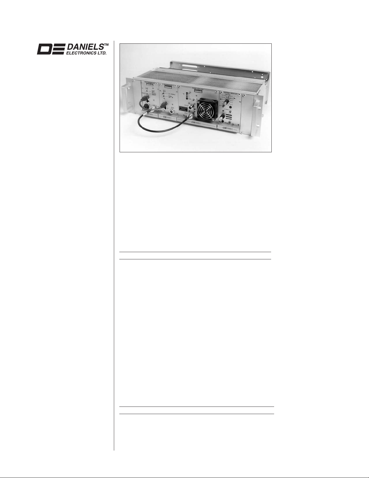
P25 DIGITAL VHF
TRANSMITTER
INSTRUCTION MANUAL
VT-4D 136-174 MHZ
Covers Models:
VT-4D140-R0-000 VT-4D160-R0-000
Copyright © 2003 Daniels Electronics Ltd. All rights reserved. No
part of this publication may be reproduced, stored in a retrieval system
or transmitted in any form or by any means, electronic, mechanical,
photocopying, recording or otherwise, without the prior written consent
of Daniels Electronics Ltd.
Document Number:
Revision:
Revision Date:
DE™ is a registered trademark of Daniels Electronic Ltd. registered in
the U.S. Patent and Trademark Offi ce.
Module Manuals Included:
IM21-VT3150AMP
IM21-001
1-0-0
Aug 2003
Daniels Electronics Ltd.
Victoria, BC
PRINTED IN CANADA
Page 2

ii
DOCUMENT CONTROL
This document has been produced, verifi ed and
controlled in accordance with Daniels Electronics’
Quality Management System requirements.
Please report any errors or problems to Daniels
Electronics’ Customer Service Department.
NOTE
The user’s authority to operate this equipment could
be revoked through any changes or modifi cations not
expressly approved by Daniels Electronics Ltd.
The design of this equipment is subject to change
due to continuous development. This equipment may
incorporate minor changes in detail from the information
contained in this manual.
P25 Digital VHF Transmitter Instruction Manual
IM21-001
Page 3

Contents
General Information ...............................................................1
Introduction ................................................................................................1
Performance Specifi cations .......................................................................2
Theory of Operation ...............................................................5
General ...................................................................................................... 5
Jumper Functions and Standard Confi guration ........................................7
Test Points .................................................................................................8
Transmitter Programming ........................................................................ 10
Transmitter Assembly and Adjustment................................. 13
Repair Note.............................................................................................. 13
Recommended Test Equipment List ........................................................14
Transmitter Assembly and Adjustment..................................................... 14
Frequency Change .................................................................................. 14
Digital Signal Processor Board Alignment ............................................... 15
iii
Repeater System Confi guration........................................... 19
Digital Repeater ....................................................................................... 19
Repeater System Troubleshooting........................................................... 20
Illustrations and Schematics ................................................ 23
P25 Digital Transmitter Front Panel......................................................... 24
P25 Digital Transmitter Block Diagram .................................................... 25
P25 Digital Transmitter Main Board Component Layout - Bottom ........... 26
P25 Digital Transmitter Main Board Component Layout - Top................. 27
P25 Digital Transmitter Schematic Diagram ............................................ 28
P25 Adapter Board Component Layout ................................................... 29
P25 Adapter Board Schematic Diagram .................................................. 29
Parts Lists ............................................................................ 31
P25 Digital Transmitter Electrical Parts List............................................. 31
P25 Digital Transmitter Mechanical Parts List ......................................... 34
P25 Adapter Board Parts List................................................................... 35
Revision History ................................................................... 37
P25 Digital VHF Transmitter Instruction Manual
IM21-001
Page 4

Manual Organization
1
GENERAL
INFORMATION
The organization of this document refl ects the
modular construction of the VT-4D family of
products. Each product is fully described within
its respective “sub-manual”; all of which are
contained within this document. In general, each
of these sub-manuals contain:
1. A functional description and specifi cation
summary.
2. A detailed technical description (Theory of
Operation).
3. Assembly, setup and alignment procedures
relevant to the particular module.
The following sub-manual is contained within
this modular manual.
VHF Amplifi er Instruction Manual: This
manual provides information on alignment
and operation of the 2 and 8 Watt RF amplifi er
modules.
The following manual is also required for
alignment of the VT-4D family transmitter.
Radio Service Software Manual: This manual
provides instructions on using the PC-based
Radio Service Software package to perform
Transmitter alignment and frequency and mode
selection. This manual is available as a PDF
fi le on CD that is supplied in the Radio Service
Software and Interface Kit.
P25 Digital VHF Transmitter Instruction Manual
IM21-001
Page 5

General Information
2
VT-4D150 Transmitter Family Models
There are four distinct models in the VT-4D150 Transmitter family each with different bands of
operation and power outputs. The four models are as follows:
• VT-4D140-2 136-150 MHz band, 0.5-2.0 Watt
• VT-4D140-8 136-150 MHz band, 2.0-8.0 Watt
• VT-4D160-2 150-174 MHz band, 0.5-2.0 Watt
• VT-4D160-8 150-174 MHz band, 2.0-8.0 Watt
The transmitters’ band of operation is determined by select components in the amplifi er.
Performance Specifi cations
Blank line
General
The following is a general set of specifi cations for the generic VT-4D150 transmitter. Additional
specifi cations, specifi c to individual modules may be found in their respective sub manuals.
Type: MT-4D Series Transmitter.
Family: VT-4D150 136 - 174 MHz.
Compatibility: MT-2, MT-3 and MT-4 Series Radio Systems, P25 interoperable.
Frequency Range: 136 to 150 MHz., 150 to 174 MHz
RF Power Output: 0.5 to 2.0 or 2.0 to 8.0 W Continuous.
Modulation: Analog: 11K0F3E or 16K0F3E (Frequency Modulation).
Project 25: 8K10F1E
System Impedance: 50 Ω; Type N connector.
Duty Cycle: 100%; Continuous operation from -30°C to +60°C.
Emissions: -70 dBc
Transmitter Mismatch Protection: 20:1 VSWR at all phase angles.
Operating Temperature Range: -30˚C to +60˚C.
Operating Humidity: 95% RH (non-condensing) at +25°C.
Operating Voltage: +13.8 Vdc Nominal (range +10 to +17 Vdc),
+9.5 Vdc Regulated.
Transmit Current: 1.7 Amps at 2 Watts RF Power Output,
2.8 Amps at 8 Watts RF Power Output
Front Panel Controls: NORM (repeat mode), OFF, and KEY TX (Tx on).
MIC MODE: ANALOG and DIGITAL.
P25 Digital VHF Transmitter Instruction Manual
IM21-001
Page 6

General Information
PTT Activation: • Active to ground; Microphone activated;
• Front Panel switch: KEY TX
PTT Time-Out-Timer: Programmable from 1 sec. to 8 hrs or infi nity. (Default 5 min.),
using Radio Service Software package.
Standby Current:
Transmitter with no Standby ≤ 75 mA
encryption modules installed
Transmitter with encryption Standby ≤ 105 mA
modules installed
DOC Type Approval: TBA
FCC Type Acceptance: TBA
Audio Specifi cations
3
Audio Input: Balanced, 600Ω or optional unbalanced input
(600 Ω or 15000Ω selectable input impedance)
Audio Response: Pre-emphasis (6 dB per octave); +1 to -3 dB
from 300 Hz to 3 kHz
Audio Deviation Limiting: +/- 2.5 kHz, +/- 5.0 kHz
Audio Distortion: < 3% THD; 1 kHz tone at 1.5 kHz or 3 kHz deviation
Hum and Noise: -34 dB typical
P25 Digital VHF Transmitter Instruction Manual
IM21-001
Page 7

This Page Intentionally Left Blank
4
Physical Specifi cations
Physical Dimensions: Width: Height: Depth:
7.1 cm (2.8 in) 12.8 cm (5.05 in) 19 cm (7.5 in)
Module Weight: 1.4 kg (3.0 lbs.)
Corrosion Prevention: Anodized aluminum construction. Stainless steel hardware.
Gold plated module connectors.
Module Design: Compact Eurostandard modular design. Plug-in modules
mate with Daniels standard M3 repeater subrack.
Subracks/modules comply with IEEE 1101, DIN 41494 and
IEC 297-3 (mechanical size / modular arrangement).
External Connections: RF Connection: type N connector located on the transmitter
module front panel. Motherboard Connections (Audio,
Power, and Control) are made through a 48 pin, gold
plated, type F connector on the rear of the transmitter
module. User connection made through mated “mother
board” assembly of the repeater subrack. Type F standard
connector complies with DIN 41612 Level 2 (200 mating
cycles, 4 day 10 ppm SO
impairment and no change in contact resistance). Digital
I/O: 8-pin RJ-45
2 gas test with no functional
Handle Text Colour: Red
P25 Digital VHF Transmitter Instruction Manual
IM21-001
Page 8

THEORY
OF OPERATION
5
P25 Digital VHF Transmitter Instruction Manual
IM21-001
Page 9

TRANSMITTER
ASSEMBLY AND ADJUSTMENT
Repair Note
13
The transmitter is mainly made up of surface
mount devices, which should not be removed
or replaced using an ordinary soldering iron.
Removal and replacement of surface mount
components should be performed only with
specifi cally designed surface mount rework
and repair stations complete with ElectroStatic
Discharge (ESD) protection.
When removing Surface Mount Solder Jumpers,
it is recommended to use solder braid in place of
manual vacuum type desoldering tools. This will
help prevent damage to the circuit boards.
P25 Digital VHF Transmitter Instruction Manual
IM21-001
Page 10

REPEATER SYSTEM
CONFIGURATION
19
P25 Digital VHF Transmitter Instruction Manual
IM21-001
Page 11

ILLUSTRATIONS
AND SCHEMATICS
Printed Circuit Board Numbering
23
Convention
Daniels Electronics Ltd. has adopted a printed
circuit board (PCB) numbering convention in
which the last two digits of the circuit board
number represent the circuit board version. All
PCB’s manufactured by Daniels Electronics Ltd.
are identifi ed by one of the following numbering
conventions:
PCB number 43-912010
Indicates circuit board version 1.0
PCB number 50002-02
Indicates circuit board version 2
(no decimal version)
P25 Digital VHF Transmitter Instruction Manual
IM21-001
Page 12
Illustrations and Schematics
24
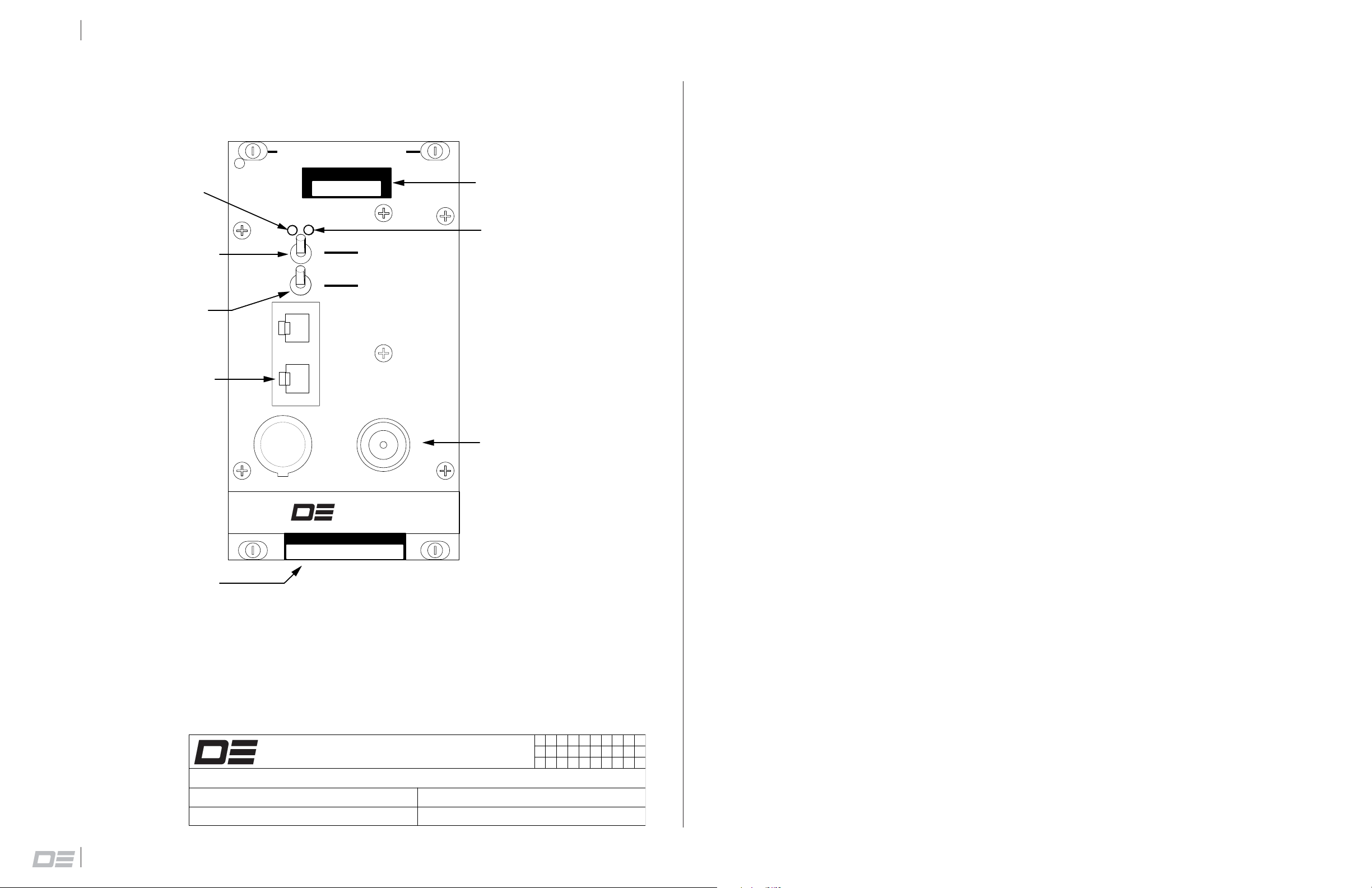
P25 Digital Transmitter Front Panel
P25 TRANSMITTER
ANALOG TRANSMIT
LED
AD
ON / OFF / KEY SWITCH
MIC MODE
MICROPHONE MODE
SELECTION SWITCH
CNTL
BUS
RJ45 CONNECTORS
FREQUENCY (MHz)
155.000
NORM
OFF
KEY TX
ANALOG
DIGITAL
A
B
FACTORY SET
OPERATING
FREQUENCY
DIGITAL TRANSMIT
LED
TRANSMITTER
MODEL IDENTIFIER
TITLE: Digital Transmitter Front Panel
MIC
DANIELS
ELECTRONICS LTD.
MADE IN CANADA
MADE IN CANADA
VT-4D150
DANIELS
ELECTRONICS LTD.
TM
RF OUT
TM
TYPE N
RF OUTPUT JACK
(Antenna)
1
2
3
4
A
11
12
13
14
21
22
23
24
5
6
7
8
9
15
16
25
26
10
17
18
19
20
27
28
29
30
DATE: 23 JUL 2003
DWG No: B0297
P25 Digital VHF Transmitter Instruction Manual
IM21-001
DRAWN BY: Bryan Harper
REV DATE: -
Page 13

P25 Digital Transmitter Electrical Parts List
31
PARTS LISTS
Ref
Desig Description Part Number
P25 Digital VHF Transmitter Instruction Manual
IM21-001
Page 14

Revision Date ECO Description
37
REVISION HISTORY
P25 Digital VHF Transmitter Instruction Manual
IM21-001
Page 15
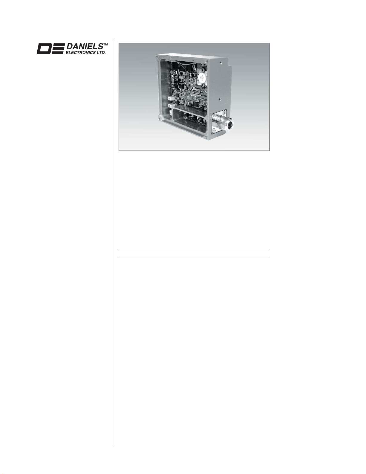
VHF TRANSMITTER
AMPLIFIER
INSTRUCTION MANUAL
VT-3 & VT-4 (132-174 MHz)
Covers Models:
A21-VPA145-08 A21-VPA165-08
Copyright © 2003 Daniels Electronics Ltd. All rights reserved. No
part of this publication may be reproduced, stored in a retrieval system
or transmitted in any form or by any means, electronic, mechanical,
photocopying, recording or otherwise, without the prior written consent
of Daniels Electronics Ltd.
Document Number:
Revision:
Revision Date:
DE™ is a registered trademark of Daniels Electronic Ltd. registered in
the U.S. Patent and Trademark Offi ce.
IM21-VT3150AMP
3-3-0
Aug 2003
Daniels Electronics Ltd.
Victoria, BC
PRINTED IN CANADA
Page 16

ii
DOCUMENT CONTROL
This document has been produced, verifi ed and
controlled in accordance with Daniels Electronics’
Quality Management System requirements.
Please report any errors or problems to Daniels
Electronics’ Customer Service Department.
NOTE
The user’s authority to operate this equipment could
be revoked through any changes or modifi cations not
expressly approved by Daniels Electronics Ltd.
The design of this equipment is subject to change
due to continuous development. This equipment may
incorporate minor changes in detail from the information
contained in this manual.
VHF Transmitter Amplifi er Instruction Manual
IM21-VT3150AMP
Page 17

RF Exposure Warning
Exposure to radio frequency (RF) energy has been identifi ed as a potential environmental factor that must be
considered before a radio transmitter can be authorized or licensed. The FCC has therefore developed maximum
permissible exposure (MPE) limits for fi eld strength and power density, listed in FCC 47 CFR § 1.1310. The
FCC has furthermore determined that determination of compliance with these exposure limits, and preparation
of an Environmental Assessment (EA) if the limits are exceeded, is necessary only for facilities, operations and
transmitters that fall into certain risk categories, listed in FCC 47 CFR § 1.1307 (b), Table 1. All other facilities,
operations and transmitters are categorically excluded from making such studies or preparing an EA, except as
indicated in FCC 47 CFR §§ 1.1307 (c) and (d).
Revised FCC OET Bulletin 65 (Edition 97-01) provides assistance in determining whether a proposed or existing
transmitting facility, operation or device complies with RF exposure limits. In accordance with OET Bulletin 65
and FCC 47 CFR § 1.1307 (b), this Daniels Electronics Ltd. transmitter is categorically excluded from routine
evaluation or preparing an EA for RF emissions and this exclusion is suffi cient basis for assuming compliance
with FCC MPE limits. This exclusion is subject to the limits specifi ed in FCC 47 CFR §§ 1.1307 (b) and 1.1310.
Daniels Electronics Ltd. has no reason to believe that this excluded transmitter encompasses exceptional
characteristics that could cause non-compliance.
Notes: • The FCC’s exposure guidelines constitute exposure limits, not emission limits. They are relevant to
locations that are accessible to workers or members of the public. Such access can be restricted or
controlled by appropriate means (i.e. fences, warning signs, etc.).
• The FCC’s limits apply cumulatively to all sources of RF emissions affecting a given site. Sites
exceeding these limits are subject to an EA and must provide test reports indicating compliance.
iii
RF Safety Guidelines and Information
Base and Repeater radio transmitters are designed to generate and radiate RF energy by means of an external
antenna, typically mounted at a signifi cant height above ground to provide adequate signal coverage. The
following antenna installation guidelines are extracted from Appendix A to OET Bulletin 65 and must be adhered
to in order to ensure RF exposure compliance:
Non-building-mounted Antennas:
Height above ground level to lowest point of antenna ≥ 10 m or
Power ≤ 1000W ERP (1640 W EIRP)
Building-mounted Antennas:
Power ≤ 1000 W ERP (1640 W EIRP)
The following RF Safety Guidelines should be observed when working in or around transmitter sites:
• Do not work on or around any transmitting antenna while RF power is applied.
• Before working on an antenna, disable the appropriate transmitter and ensure a
“DO NOT USE” or similar sign is placed on or near the PTT or key-up control.
• Assume all antennas are active unless specifi cally indicated otherwise.
• Never operate a transmitter with the cover removed.
• Ensure all personnel entering a transmitter site have electromagnetic energy awareness
training.
For more information on RF energy exposure and compliance, please refer to the following:
[1] FCC Code of Regulations; 47 CFR §§ 1.1307 and 1.1310.
[2] FCC OET Bulletin 65, Edition 97-01, “Evaluating Compliance with FCC Guidelines for
Human Exposure to Radiofrequency Electromagnetic Fields”.
[3] http://www.fcc.gov/oet/rfsafety/
VHF Transmitter Amplifi er Instruction Manual
IM21-VT3150AMP
Page 18

Contents
General Information ...............................................................5
Introduction ................................................................................................ 5
Performance Specifi cations .......................................................................6
Theory of Operation ..............................................................7
Amplifi er Operation ....................................................................................7
Power Requirements .................................................................................8
VHF Transmitter Amplifi er Current Consumption ........................................... 8
RF Circuitry ................................................................................................8
VHF Transmitter Amplifi er Lowpass Filter ...................................................... 8
Power Control Circuitry ..............................................................................8
Power Sensing Circuitry............................................................................. 8
Output Power Sense ...................................................................................... 9
VSWR Sense.................................................................................................. 9
VSWR Overload ............................................................................................. 9
v
VHF Transmitter Amplifi er Alignment ....................................11
Repair Note.............................................................................................. 11
Recommended Test Equipment List ........................................................12
General .................................................................................................... 12
Standard Factory Settings and Jumper Confi guration ............................. 13
VHF Transmitter Amplifi er Alignment .......................................................13
VHF Transmitter Amplifi er Adjustment .......................................................... 13
General Set-Up............................................................................................. 14
Output Power Alarm (Forward Power).......................................................... 14
Output Power................................................................................................ 15
Antenna VSWR Alarm (Reverse Power) ...................................................... 15
Antenna VSWR Overload............................................................................. 16
Procedure Verifi cation .................................................................................. 16
Illustrations and Schematics ................................................ 17
VT-3/150 Tranmitter Amplifi er Component Layout................................... 18
VT-3/150 Tranmitter Amplifi er Schematic Diagram.................................. 19
VT-3/150 Amplifi er Low Pass Filter Component Layout........................... 20
VT-3/150 Amplifi er Low Pass Filter Schematic Diagram.......................... 20
Parts Lists ............................................................................ 21
VHF Transmitter Amplifi er Electrical Parts List ........................................ 21
VHF Transmitter Amplifi er Mechanical Parts List..................................... 24
Revision History ................................................................... 25
VHF Transmitter Amplifi er Instruction Manual
IM21-VT3150AMP
Page 19

Introduction
1
GENERAL
INFORMATION
The VHF Transmitter Amplifi er provides the
fi nal stage of RF amplifi cation and fi ltering for
the entire VHF Transmitter VT-3 132 - 174
MHz family and the VT-4 P25 Digital VHF
Transmitters. The amplifi er has two distinct
frequency ranges: 132 to 150 MHz, and 150 to
174 MHz with continuously adjustable 2.0 to 8.0
Watts output power. This Amplifi er is housed in a
machined aluminum case that ensures optimum
RF shielding, provides a good ground, and also
acts as a heatsink.
Additionally, the VHF Transmitter Amplifi er is
equipped with output power and VSWR sensing
lines that can be individually confi gured as open
collector or linear outputs. The internal VSWR
sensor protects the amplifi er from high antenna
VSWR by approximately halving the amplifi er’s
RF gain when a VSWR overload condition is
present.
The Lowpass Filter Board provides output
fi ltering for the VHF Transmitter Amplifi er.
The Lowpass fi lter assembly is mounted in a
separate compartment of the amplifi er case
in order to provided maximum attenuation of
harmonic and other spurious signals.
VHF Transmitter Amplifi er Instruction Manual
IM21-VT3150AMP
Page 20

General Information
2
Performance Specifi cations
Type: VHF Transmitter Amplifi er module for VT-3/150 , VT-4R and VT-4B series
transmitters.
Compatibility: MT-3 series FM Transmitter Main Board or
MT-4 P25 Digital Transmitter Main Board.
Frequency Range: 132-150 MHz or 150-174 MHz.
RF Power Output: adjustable 2.0 to 8.0 Watts
RF power Input: nominal level adjustable from 0 dBm to +5 dBm, held within
+/- 2 dB of nominal.
Output Impedance and VSWR: 50 Ω, Type N connector; 3:1 max. VSWR.
Input /Output Isolation: > 60 dB
Duty Cycle: 100%: Continuous operation from -40˚ C to +60˚C.
Harmonic Emissions: < -90 dBc.
Transmitter Mismatch Protection: 20:1 VSWR at all phase angles.
Transmitter Alarm: Forward power sense and reverse VSWR;
- open collector output (separate or ‘OR’ed confi guration);
- linear output (separate lines only).
Operating Temperature Range: -30˚ C to +60˚ C, optional -40˚ C temperature test.
Operating Humidity: 95% RH (non-condensing) at +25˚ C.
Operating Voltage: +13.8 Vdc Nominal (range +11 to +16 Vdc),
+9.5 Vdc Regulated.
Amplifi er Standby Current: < 0.5 mA.
Amplifi er Enable: Active to ground.
Amplifi er Enable Response: typically overdamped, rising to within 90% of full power within 5 msec;
maximum (underdamped) overshoot of 30%.
VHF Transmitter Amplifi er Instruction Manual
IM21-VT3150AMP
Page 21

THEORY
OF OPERATION
3
VHF Transmitter Amplifi er Instruction Manual
IM21-VT3150AMP
Page 22

VHF TRANSMITTER
AMPLIFIER ALIGNMENT
Repair Note
7
The VHF Transmitter Amplifi er is mainly made
up of surface mount devices that should not be
removed or replaced using an ordinary soldering
iron. Removal and replacement of surface
mount components should be performed only
with specifi cally designed surface mount rework
and repair stations complete with Electrostatic
Dissipative (ESD) protection.
When removing Surface Mount Solder Jumpers,
it is recommended to use solder braid in place of
manual vacuum type desoldering tools. This will
help prevent damage to the circuit boards.
VHF Transmitter Amplifi er Instruction Manual
IM21-VT3150AMP
Page 23

ILLUSTRATIONS
AND SCHEMATICS
Printed Circuit Board Numbering
17
Convention
Daniels Electronics Ltd. has adopted a printed
circuit board (PCB) numbering convention in
which the last two digits of the circuit board
number represent the circuit board version. All
PCB’s manufactured by Daniels Electronics Ltd.
are identifi ed by one of the following numbering
conventions:
PCB number 43-912010
Indicates circuit board version 1.0
PCB number 50002-02
Indicates circuit board version 2
(no decimal version)
VHF Transmitter Amplifi er Instruction Manual
IM21-VT3150AMP
Page 24

VHF Transmitter Amplifi er Electrical Parts List
17
PARTS LISTS
Ref
Desig Description Part Number
VHF Transmitter Amplifi er Instruction Manual
IM21-VT3150AMP
Page 25

Revision Date ECO Description
21
REVISION HISTORY
VHF Transmitter Amplifi er Instruction Manual
IM21-VT3150AMP
 Loading...