

Page 1

X-2 HF SSB Transceiver
Technical service manual
1992, 1993 Codan Pty Ltd.
ACN 007 590 605
Order code 15-02047
Issue 2, October 1993
Page 2

Head Office International Marketing Offices
Codan Pty Ltd
81 Graves Street
Newton
SOUTH AUSTRALIA 5074
Telephone
National 08 336 0311
International +61 8 336 0311
Facsimile 08 337 6090
Australia, Pacific and South East Asia
Codan Pty Ltd
Suite 24, 818 Pittwater Road
Dee Why
New South Wales
AUSTRALIA 2099
Telephone
National 02 971 2233
International +61 2 971 2233
Facsimile 02 982 1117
Telex 22631
Africa, Europe and The Middle East
Codan (U.K.) Ltd
6 Grove Park
Mill Lane
Alton, Hampshire GU34 2QG
UNITED KINGDOM
Telephone
National 0420 80121
International +44 420 80121
Facsimile 0420 541098
Telex 858355
North and South America
Codan Pty Ltd
Suite 101
8011 Leslie Road
Richmond BC V6X 7E4
CANADA
Telephone
National 604 270 8332
International +1 604 270 8332
Facsimile 604 270 4401
Page 3

Publication No: 15-02047
Table of Contents
1 Introduction........................................................................................................1-1
1.1 Purpose...........................................................................................................1-1
1.2 How this manual is organised.......................................................................... 1-1
1.3 Conventions....................................................................................................1-2
1.4 Related Documents......................................................................................... 1-2
1.5 Overview ........................................................................................................1-2
1.6 Specifications.................................................................................................. 1-3
1.6.1 General Specifications.................................................................1-3
1.6.2 Receiver Specifications...............................................................1-5
1.6.3 Transmitter Specifications...........................................................1-6
2 Brief Description............................................................................................2-1
2.1 General...........................................................................................................2-1
2.2 Control and Switching.....................................................................................2-2
2.3 Synthesiser......................................................................................................2-2
2.4 Receive Path...................................................................................................2-3
2.5 Transmit Path..................................................................................................2-4
3 Operating Instructions...............................................................................3-1
4 Technical Description................................................................................4-1
4.1 Control and Supply Voltages...........................................................................4-2
4.1.1 Power .........................................................................................4-2
4.1.2 Supply Voltages .........................................................................4-2
4.1.3 Receive/Transmit Switching........................................................4-3
4.2 Receiver..........................................................................................................4-4
4.2.1 Input Filters................................................................................4-4
4.2.2 First Mixer.................................................................................. 4-4
4.2.3 45 MHz Roofing Filter................................................................4-4
4.2.4 Second Mixer.............................................................................4-4
4.2.5 Noise Limiter..............................................................................4-5
4.2.6 455 kHz Filter and IF Amplifier..................................................4-5
4.2.7 Automatic Gain Control.............................................................. 4-6
4.2.8 Mute........................................................................................... 4-7
4.2.9 Volume Control and Audio Amplifier .........................................4-8
Page 4

ii Table of Contents X-2 Technical Service Manual
Publication No: 15-02047
4.3 Transmitter Exciter ......................................................................................... 4-8
4.3.1 Microphone Compressor.............................................................4-8
4.3.2 Modulator .................................................................................. 4-9
4.3.3 455 kHz Filter and First Mixer.................................................... 4-9
4.3.4 45 MHz Roofing Filter................................................................4-9
4.3.5 Second Mixer and Exciter Output Filter......................................4-9
4.4 Local Oscillators...........................................................................................4-10
4.4.1 Introduction..............................................................................4-10
4.4.2 VCO1 and PLL ........................................................................4-10
4.4.3 VCO2 and PLL ........................................................................4-11
4.4.4 455 kHz Local Oscillator.......................................................... 4-12
4.4.5 Clarifier....................................................................................4-12
4.5 Micro and Peripherals ...................................................................................4-13
4.5.1 Microcontroller......................................................................... 4-13
4.5.2 I2C Bus ....................................................................................4-13
4.5.3 PA Control Bus........................................................................4-13
4.5.4 Front Panel Controls .................................................................4-14
4.5.5 Tune......................................................................................... 4-15
4.5.6 Tone Generation....................................................................... 4-15
4.5.7 A/D Inputs................................................................................ 4-15
4.5.8 Microcontroller Reset...............................................................4-16
4.6 PA and Filters ............................................................................................... 4-16
4.6.1 Gain Control Stage................................................................... 4-17
4.6.2 Predriver Stages .......................................................................4-17
4.6.3 Driver Stage.............................................................................4-17
4.6.4 Output Stage and Bias Regulator..............................................4-18
4.6.5 Output Filters and Antenna 1 and 2 Select ................................4-18
4.6.6 ALC Control ............................................................................4-18
5 Maintenance.......................................................................................................5-1
5.1 Introduction....................................................................................................5-1
5.2 General...........................................................................................................5-1
5.2.1 CMOS Devices ...........................................................................5-1
5.2.2 Circuit Boards ............................................................................5-2
5.2.3 Transmitter Precautions..............................................................5-3
5.2.4 Probe Precautions.......................................................................5-4
5.3 Fault Diagnosis ............................................................................................... 5-4
5.3.1 General.......................................................................................5-4
5.3.2 Voltage measurements................................................................ 5-5
5.3.3 No Reception .............................................................................5-6
Page 5

X-2 Technical Service Manual iii
Publication No: 15-02047
5.3.4 Transmitter Failure ..................................................................... 5-7
5.3.5 Unlocked Synthesiser.................................................................. 5-7
5.3.6 PA Failure ..................................................................................5-8
5.4 Dismantling and Assembling ............................................................................5-8
5.4.1. General.......................................................................................5-8
5.4.2 Top and Bottom Covers ............................................................. 5-9
5.4.3 Rx/Exciter & Control PCB .........................................................5-9
5.4.4 Front Panel PCB .........................................................................5-9
5.4.5 PA and Filter Assembly.............................................................5-10
5.4.6 Replacement of PA Transistors.................................................5-11
6 Channel Additions.........................................................................................6-1
7 Adjustments....................................................................................................... 7-1
7.1 Introduction....................................................................................................7-1
7.2 Test Equipment Required................................................................................ 7-1
7.3 Voltage Regulators ......................................................................................... 7-1
7.4 Crystal Oven................................................................................................... 7-2
7.5 Test Mode ......................................................................................................7-2
7.6 VCO Checks and Adjustments ........................................................................ 7-4
7.6.1 VCO1 Check..............................................................................7-4
7.6.2 VCO2 Check..............................................................................7-4
7.6.3 VCO2 Adjust.............................................................................. 7-5
7.7 45 MHz Filter Alignment.................................................................................7-5
7.7.1 Alignment - Method 1................................................................. 7-6
7.7.2 Alignment - Method 2................................................................. 7-7
7.8 455 kHz IF and N/L Alignment....................................................................... 7-7
7.9 Frequency Adjustment..................................................................................... 7-8
7.9.1 Frequency Adjust USB...............................................................7-8
7.9.2 Frequency Adjust LSB................................................................7-9
7.10 Mute Adjustment.............................................................................................7-9
7.11 PA Adjustments.............................................................................................7-10
7.11.1 Driver Bias...............................................................................7-10
7.11.2 PA Bias....................................................................................7-10
7.11.3 Output Power...........................................................................7-11
7.11.4 Intermodulation........................................................................7-12
7.12 Receiver Performance Checks........................................................................7-13
7.12.1 Sensitivity and S+N/N ratio ......................................................7-13
7.12.2 AGC Check..............................................................................7-13
7.12.3 Audio Output ...........................................................................7-13
Page 6

iv Table of Contents X-2 Technical Service Manual
Publication No: 15-02047
7.12.4 Selectivity (USB operation)......................................................7-13
7.12.5 Clarifier Operation....................................................................7-14
7.12.6 Noise Limiter Operation ...........................................................7-14
7.13 Transmitter Performance Checks ................................................................... 7-14
7.13.1 Frequency Check...................................................................... 7-14
7.13.2 ALC.........................................................................................7-15
7.13.3 Power Output and Intermodulation...........................................7-15
7.13.4 Emergency Call ........................................................................7-15
8 Appendices.........................................................................................................8-1
Appendix A: Connectors ..........................................................................................8-1
A.1 Microphone................................................................................8-1
A.2 External Loudspeaker.................................................................8-1
A.3 Antenna Control......................................................................... 8-2
A.4 Programming Cable....................................................................8-2
A.5 Cloning Cable.............................................................................8-2
Appendix B: Parts Lists............................................................................................8-3
B.1 General Information....................................................................8-3
B.2 Ordering Information..................................................................8-4
B.3 Component Substitution .............................................................8-4
B.4 Parts Lists ...................................................................................8-4
Appendix C: Engineering Drawings........................................................................8-23
Appendix D: Glossary of Terms..............................................................................8-25
D.1 Abbreviations ...........................................................................8-25
D.2 Abbreviations of Units.............................................................. 8-26
D.3 Abbreviations of Unit Multiples................................................8-27
Page 7

X-2 Technical Service Manual v
Publication No: 15-02047
List of figures
Figure Description Page No
2.1 X-2 PCB Block Diagram 2-1
7.1 Ripple Response 7-6
List of tables
Table Description Page No
2.1 Drawing Reference 2-1
3.1 Audible Warning Tones 3-2
4.1 Drawing Reference 4-1
4.2 Rx/Exciter PCB Supply Voltages 4-2
4.3 PA PCB Supply Voltages 4-2
5.1 Peak to Peak Voltages 5-8
7.1 USB/LSB Test Frequencies and Functions 7-3
7.2 Power Output PEP vs Measuring Instrument 7-11
A.1 Microphone Connector Pin Function 8-1
A.2 External Loudspeaker Connector Pin Function 8-1
A.3 Antenna Control Connector Pin Function 8-2
A.4 Programming Cable Connector Pin Function 8-2
A.5 Cloning Cable Connector Pin Function 8-2
B.1 Resistor and Capacitor Abbreviations 8-3
B.2 Parts List Index 8-4
C.1 List of Drawings 8-24
D.1 Abbreviations 8-26
D.2 Abbreviations of Units 8-27
D.3 Abbreviations of Unit Multiples 8-28
Page 8

vi Table of Contents X-2 Technical Service Manual
Publication No: 15-02047
Page 9

X-2 Technical Service Manual 1-1
Publication No: 15-02047
1 Introduction
1.1 Purpose
The purpose of this manual is to provide a technical description, details and
drawings about the X-2 transceiver for the technician to understand the:
• function
• technical operation
• fault diagnosis
• dismantling and assembly
• setup and adjustment procedures
1.2 How this manual is organised
The X-2 Technical Service Manual is organised as follows:
Chapter 1
An overview of the features of the X-2 transceiver
including specifications.
Chapter 2
A brief description of the X-2 transceiver with a general
description of the major circuit functions for the control,
reception and transmission of signals.
Chapter 3
Operating instructions for the X-2 transceiver.
Chapter 4
A more detailed technical description of the operation
and circuit function of the X-2 transceiver. Read this
with the associated technical drawings found in the
appendices.
Chapter 5
Maintenance, general cautions and warnings, fault
diagnosis procedures associated with the maintenance of
the X-2 transceiver.
Chapter 6
Programming procedures for channel additions.
Chapter 7
Adjustments, checks and alignments to the X-2
Transceiver detailing required test equipment.
Chapter 8
Comprises four appendices. Connector tables, parts lists,
engineering drawings and glossaries.
Page 10

Introduction 1-2 X-2 Technical Service Manual
Publication No: 15-02047
1.3 Conventions
The X-2 transceiver is type approved in Australia as the 9105 transceiver. All
type approval documentation refers to it as the 9105. Throughout this
manual the transceiver is referred to as the X-2.
1.4 Related Documents
If there is a need to program the X-2, make reference to the XP
programming guide. This guide is available as a separate document, Codan
Part No:15-04035.
1.5 Overview
The X-2 is a 10 channel, high frequency single sideband (HF SSB)
transceiver suitable for use in fixed station or mobile applications.
The X-2 can be factory set or dealer programmed using the XP programming
system to select:
• operating frequencies
• mode of operation
• emergency calling
• one of two antenna output sockets.
This programming feature eliminates the need for crystals and discreet
channelling/customising components. Because operation on lower sideband
(LSB), upper sideband (USB) or Emergency Call (Royal Flying Doctor
Service RFDS - only in Australia) is software programmable, there is no
need for factory fitted hardware options.
Different audio tones indicate operating conditions or system faults such as:
• excessive VSWR
• tune complete or fail
• low or high supply voltage
• channel not programmed.
Where two channel networks are used, two separate antenna output sockets
on the rear panel allow the use of:
• individually tuned half-wave dipole base station antennas
• mobile whips.
This eliminates the need for antenna selectors or coaxial switches.
Users can clone the programmed information contained in the X-2 to another
transceiver by using the microphone socket. XP software is not required for
cloning.
Page 11

X-2 Technical Service Manual Introduction 1-3
Publication No: 15-02047
1.6 Specifications
This section of the manual provides specifications for the X-2 transceiver in
the following categories:
• General Specifications
• Receiver Specifications
• Transmitter Specifications
The specification figures listed are the minimum standard for the X-2
transceiver and production models will equal or exceed these figures. Where
relevant, acceptance limits are shown in brackets.
Unless otherwise specified, all measurements have been made using
13.6 V DC, with 50 Ω source and load resistances at an ambient temperature
of 25°C.
1.6.1 General Specifications
Frequency Range
2 to 18 MHz.
Channel Capacity
10 channels. Any combination of single or dual
frequency simplex.
Frequency Generation
Frequency synthesiser with 10 Hz resolution:
controlled by plug-in EEPROM.
Operating Modes
Single sideband (J3E).
Programmable USB, LSB or front panel
switched.
Frequency Stability
USB: ±2(3)ppm
LSB: ±(2(3)ppm +10 Hz)
}-10°C to +60°C
Long term ageing 1ppm per year.
Crystal reference oven warm up time 1 minute.
Programming
Frequencies and options are programmed via the
microphone socket and 3-wire RS232 interface
using XP programming software and an IBM
compatible PC.
Cloning
Channel frequencies and options can be copied
from one transceiver to another via the
microphone socket.
Controls
Power ON/OFF and Volume.
Channel select.
Clarifier.
Mode USB/LSB.
Mute ON/OFF/Tune.
Emergency Call: RFDS 880/1320 Hz. (Australia
only)
Page 12

Introduction 1-4 X-2 Technical Service Manual
Publication No: 15-02047
Indicators
Power On/Transmit.
Connectors:
Front
Rear
Microphone/Handset.
RF - UHF connectors: Qty 2 (programmable).
Antenna Control.
Extension Loudspeaker.
RF Input/Output
impedance
50 Ω nominal.
Supply Voltage
12 V DC nominal, negative earth.
Normal operating range 10.5 to 15 V.
Maximum operating range 9 to 16 V approx.
Reverse polarity protection.
Supply Current
Receive : no signal 360 mA.
Transmit: refer to Transmit Specifications.
Environment
Ambient Temp.
-10°C to +30°C
+30°C to +60°C
Relative Humidity
95%
From 95% at +30°C to
30% at +60°C
Derate upper ambient temperature by 1°C per
330 m above sea level.
Cooling
Convection.
Size and Weight
Transceiver only:
230 mm W x 75 mm H x 290 mm D 2.5 kg
With mounting cradle:
250 mm W x 90 mm H x 290 mm D 3.0 kg
Depth measurements include rear
connectors/cables.
Page 13

X-2 Technical Service Manual Introduction 1-5
Publication No: 15-02047
1.6.2 Receiver Specifications
Type
Dual conversion, superheterodyne.
IF Frequencies
45 MHz and 455 kHz.
Sensitivity
0.3(0.4) µV PD -117(-115) dBm for 10 dB
SINAD with > 50 mW audio output.
Input Protection
Will withstand 50 V RF from 50 Ω.
Selectivity
Greater than 70(65) dB at -1 kHz and +4 kHz
reference SCF USB.
Pass Band -6(-8) dB 300 to 2700 Hz
Ripple 2(4) dB pp 500 to 2500 Hz
Desensitisation
10 dB SINAD reduced to 7 dB SINAD.
-1 and +4 kHz (ref SCF) 65(60) dB
±10 kHz 85(80) dB
±50 kHz 100(95) dB
Image Rejection
Better than 90(80) dB.
Spurious Responses
Better than 90(70) dB.
Self Generated Signals > 0.3 µV PD:
3652, 5478, 7304, 9130, 10956, 14608 kHz.
Cross Modulation
A signal 85(80) dB above a signal producing
10 dB SINAD, modulated 30% and removed at
least 20 kHz from the wanted signal will
produce an increase in receiver noise of less than
3 dB.
Blocking
As for desensitisation.
Intermodulation
To produce a third order intermodulation
product equivalent to a wanted signal producing
10 dB SINAD, two unwanted signals greater
than 30 kHz removed from the wanted signal
must have a level greater than 82(80) dB above
the wanted signal. Third order intercept +7(4)
dBm, not affected by AGC.
AGC
Less than 6 dB variation in output for input
variation between 1.5(2.5) µV and 100 mV PD.
Fast attack, slow release.
AF Power and
Distortion
2.5 W into 8 Ω 5% THD
5.0 W into 4 Ω 5% THD
8.0 W into 2 Ω 5% THD.
Clarifier
±50 Hz up to 5 MHz
±10 ppm above 5 MHz
Clarifier is automatically reset to mid-frequency
with channel change.
Page 14

Introduction 1-6 X-2 Technical Service Manual
Publication No: 15-02047
1.6.3 Transmitter Specifications
Type
All solid state.
Power Output
100 W PEP ± 0.5 dB may be internally set to
any output between 125 and 25 W PEP.
CW or single tone approx. 60% of PEP.
(Average ALC control).
Duty Cycle
100% normal speech.
Supply Current
2-tone/CW 8 to 12 A
Average speech 6 A
Average speech for battery life calculations.
Protection
Safe under all load conditions by limiting
reflected power to 10 W PEP and limiting PA
transistor collector voltage swing.
Thermal protection against excessive heatsink
temperature.
AF Response
Overall response of microphone and transmitter
rises approximately 6 dB/octave 300-2700 Hz.
Electrical input -6(8) dB, 300-2700 Hz.
Ripple 2(4) dB pp, 500-2500 Hz.
Spurious and
Harmonic Emissions
55(48) dB below PEP.
Carrier Suppression
60(50) dB below PEP.
Unwanted Sideband
50(45) dB below PEP (400 Hz).
70(65) dB below PEP (1 kHz).
Intermodulation
(2 tone test)
100 W 30(26) dB below each tone.
36(32) dB below PEP.
125 W 27(26) dB below each tone.
33(32) dB below PEP.
ALC
A 10 dB increase in signal input above
compression threshold produces less than 0.5 dB
increase in power output.
Maximum ALC range greater than 30 dB.
ALC attack time approximately 1 ms.
Residual Noise
65(55) dB below PEP of selected channel.
Microphone
Dynamic type with push-to-talk switch fitted in
the case.
n
Page 15
X-2 Technical Service Manual 2-1
Publication No: 15-02047
2 Brief Description
This section of the manual provides a brief description of the major
components and circuit functions of the X-2 transceiver as follows:
• Control and switching functions
• Synthesizer operation
• Receive path
• Transmit path
For an in-depth review of these functions refer to Chapter 4 "Technical
Description".
2.1 General
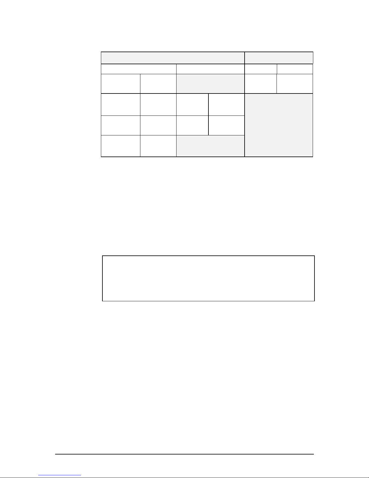
Read this description of the X-2 transceiver with the circuit drawing shown
in Table 2.1.
Title Circuit Diagram
X-2 Block Diagram 03-00876
Table 2.1: Drawing reference
The X-2 transceiver is a double conversion superheterodyne receiver. It uses
45 MHz and 455 kHz IF frequencies for the double conversion process. The
45 MHz roofing filter and the 455 kHz sideband filter are common to the
transmit and receive audio paths.
The transceiver can be programmed with channels for either single or dual
frequency simplex operation, and uses the double conversionError!
Bookmark not defined. process when transmitting or receiving.
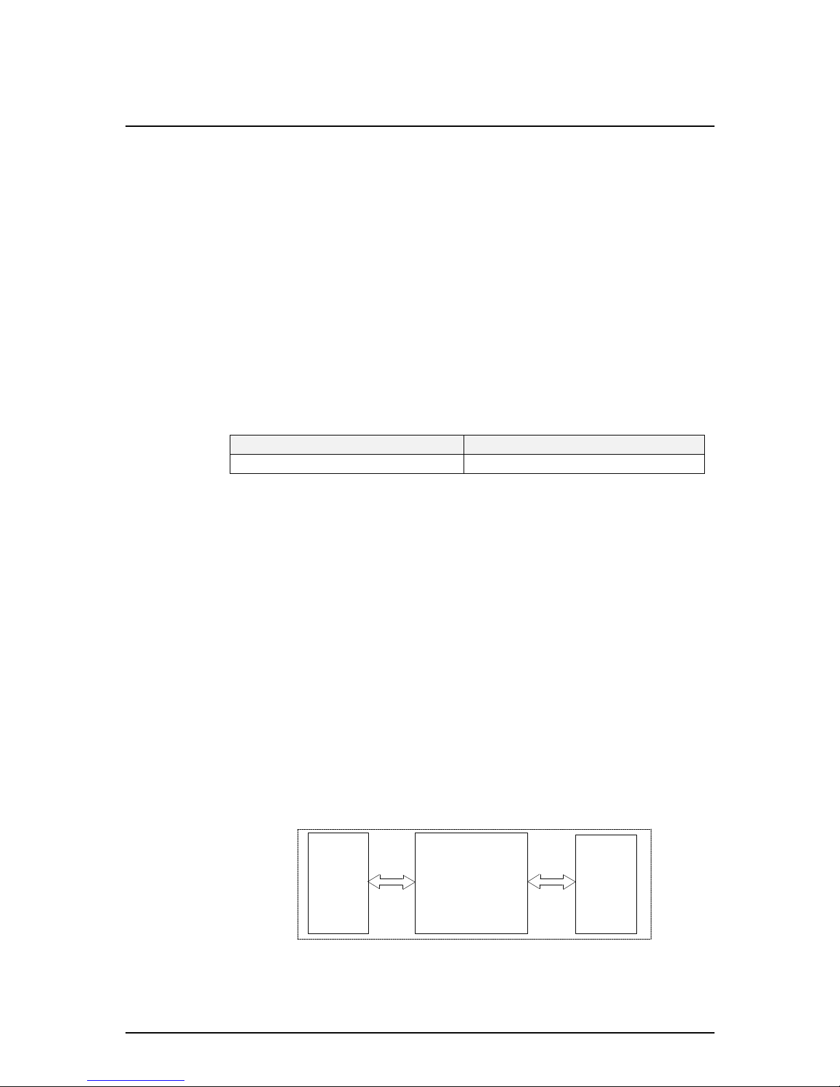
The X-2's circuits and functions are located on three major PCBs as shown in
Figure 2.1.
• Front panel PCB and panel controls
• Rx/Exciter & Control Circuit PCB consisting of:
- RF and Dual synthesizer circuits
- 455 kHz IF and audio circuits
- Microprocessor and peripheral circuits
• PA and Filter PCB.
Front
Panel
PA &
Filters
Receiver\Exciter
and Control
Figure 2.1: X-2 PCB Block Diagram
Page 16

Brief Description 2-2 X-2 Technical Service Manual
Publication No: 15-02047
The main elements of the X-2 can be divided into the control and switching
functions, the synthesizers used to produce the oscillator frequencies and the
signal paths taken in receive and transmit modes.
Circuit elements and functions common to both the transmit and receive
paths are the:
• 45 MHz roofing filter
• 455 kHz sideband filter
• local oscillators VCO1 and VCO2
2.2 Control and Switching
The switching and control voltages determine the path taken by the transmit
or receive signals through the transceiver.
Most of the transceiver functions are controlled by microcontroller IC403.
Channel frequencies and options are programmed via the microcontroller to
the Electrical Erasable Programmable Read Only Memory (EEPROM),
IC404. All other transceiver functions are pre-programmed in the
microcontroller's internal Read Only Memory (ROM).
The power on/off and volume controls are hardware functions and not
controlled by the microcontroller.The on/off switch is part of the volume
control and directly energises a power-on relay. A series diode provides
reverse polarity protection.
The volume control in the audio signal path connects the preamplifier (after
the demodulator) and the audio amplifier to drive the loudspeaker.
2.3 Synthesizer
The X-2 transceiver uses single loop synthesizers. The main synthesizer
(VCO1) generates an oscillator frequency of 47 MHz to 63 MHz i.e. 2 MHz
to 18 MHz plus 45 MHz, in 2 kHz steps.
The vernier synthesizer (VCO2) generates oscillator frequencies of
44.5435 MHz to 44.5455 MHz in 10 Hz steps.
The microcontroller IC controls the synthesizers by loading serial data into
both synthesizers. The data varies according to the required channel
frequency programmed into the memory.
When the upper sideband is selected, the X-2 uses one main reference
oscillator of 7304 kHz to produce 456.5 kHz (7304 kHz divided by 16). If
lower sideband is needed, a second crystal of 1814 kHz is used to provide
453.5 kHz (1814 kHz divided by 4).
Page 17

X-2 Technical Service Manual Brief Description 2-3
Publication No: 15-02047
2.4 Receive Path
PA and Filter PCB
The received signal from the antenna passes through a PA low-pass filter to
the transmit/receive relay and broadcast filter on the PA PCB to the receiver
input on the main PCB.
Rx/Exciter & Control PCB
From the receive input, the signal is fed via a second 20 MHz low-pass filter
to the input of the first balanced mixer. Here it mixes with the local
oscillator VCO1 and converts to 45 MHz.
A 15 kHz roofing filter filters this 45 MHz signal before being applied to the
second balanced mixer. The signal mixes with a second local oscillator
VCO2 producing an IF signal centred on 455 kHz.
The output of the second mixer divides into two paths:
• the main path passes through a noise gate to a 2.5 kHz sideband filter
where only the wanted sideband passes to the high gain AGC controlled
IF amplifier.
• the second path passes the signal through an amplifier which detects
noise and controls the noise gate to remove impulse noise such as car
ignition from the 455 kHz signal.
The amplified 455 kHz signal is demodulated to produce an audio signal and
amplified. The amplified audio signal operates an AGC circuit. This
controls the IF amplifier gain to prevent overloading when receiving strong
signals. It is also used to maintain a constant audio output with changing
input signals.
After amplification the signal passes through a mute that removes the
receiver noise from the speaker when enabled. When speech is detected, the
gate in the audio line closes to allow the signal to be heard. The signal feeds
the volume control on the Front Panel PCB.
Front Panel PCB
The signal from the volume control is applied to a power amplifier IC2 to
drive the transceiver's loudspeaker.
Page 18

Brief Description 2-4 X-2 Technical Service Manual
Publication No: 15-02047
2.5 Transmit Path
Rx/Exciter PCB
The microphone amplifier/compressor IC303/306, amplifies and levels the
audio signal from the microphone and drives a balanced modulator IC301.
When mixed with the local oscillator, the double sideband output of the
modulator feeds a 2.5 kHz sideband filter centred on 455 kHz, passing only
the wanted sideband to the first mixer IC9. Here it mixes with the local
oscillator VCO2 to produce an IF signal of 45 MHz.
The 15 kHz wide roofing filter centred at 45 MHz filters the transmit signal
to remove unwanted mixed signals before it feeds the second mixer.
At the second mixer, the signal mixes with the oscillator VCO1 producing
the required channel frequency (2 MHz to 18 MHz) and passes through a
20 MHz low pass filter to the Power Amplifier & Filter PCB (PA PCB).
PA and Filter PCB
The PA assembly amplifies the signal, passes it on to the transmit/receive
relay, and then to the selected band filter. At the filter output it continues to
the VSWR detector. The detector monitors the forward and reflected power
and controls the power output of the transmitter. If a high VSWR is
detected, the power output reduces to protect the power amplifier.
A coaxial cable connects the signal to the appropriate antenna for
transmission.
n
Page 19

X2 Technical Service Manual 3-1
Publication No: 15-02047
3 Operating Instructions
This section of the maual describes how to operate the X-2 Tansceiver in
both normal and RFDS Emergency Call (Australia only) modes. Table 3.1
provides an explanation of the meaning of audible tones. To operate the X-2:
1. Switch the transceiver on by turning the Volume control clockwise
until the indicator lamp lights.
2. Select the required Channel and USB or LSB mode.
3. If using a broadband or dipole antenna go to step 5.
4. After selecting the required channel:
(i) Where a multi-frequency tapped whip is used, select the correct
tap position for the frequency in use.
(ii) Where an automatic antenna tuner is used, select Tune for
approximately one second and ensure the "tune complete",
double high beep is heard.
(iii) Where a manual antenna tuner is being used, set the tuner
controls to the logging scale positions. Before transmitting
operate the Tune switch and adjust the Tune control on the
front panel for maximum meter reading.
5. With the Mute switch in the Off position, set the Volume control to a
comfortable listening level. The mute function removes background
noise when no signals are present and should be switched Off to
prevent occasional loss of syllables when communicating in the
presence of weak signals.
6. Adjust the Clarifier to obtain a better speech quality if necessary.
7. Listen before transmitting to ensure that the selected Channel is free
of traffic.
8. Hold the Microphone side-on, close to the mouth. Press the
Transmit button and speak clearly.
9. When transmitting, the Indicator light will flicker. Tune will cause the
Indicator to light continuously.
10. Audible tones are provided to inform the operator of equipment status
or provide an operating error warning as shown in Table 3.1.
Page 20
Operating Instructions 3-2 X-2 Technical Service Manual
Publication No: 15-02047
BEEPS CONTINUOUS
Low Tone High Tone Low Tone High Tone
Single
Transmit
inhibited
Channel
unavailable
High supply
voltage
Double
Tune Fail
(check
antenna)
Double
Tune
complete
Slow repetitive
Low supply
voltage
Repetitive
Channel not
programmed
Fast repetitive
PTT time out
Table 3.1: Audible Warning Tones
11. If making an RFDS Emergency Call (Australia only) carry out the
steps as outlined in 1 to 5 and proceed as follows:
(i) Ensure a local RFDS channel has been selected - on other
channels the call will not be transmitted.
(ii) Operate Emgcy Call switch for at least 15 seconds then wait for
a reply before transmitting. Unattended RFDS base stations will
transmit a tone within 90 seconds if the call has been received.
ICAUTION
1. Do not obstruct the free flow of air through the transceiver rear fins.
2. If using two antennas, connect them to the correct antenna sockets for
the frequency being used.
n
Page 21

X2 Technical Service Manual 4-1
Publication No: 15-02047
4 Technical Description
This section of the manual contains a technical description of the X-2
transceiver and should be read together with the drawings shown in
Table 4.1.
Description Circuit Diagram PCB Assembly
Rx/Exciter & Control 04-02907 (3 sheets) 08-04840
-RF and Dual Synthesizer Sheet 1
-455 kHz IF and Audio Sheet 2
-Micro and Peripherals Sheet 3
PA and Filter 04-02908 08-04841
Front Panel 04-02909 08-04842
Table 4.1: Drawing reference Directory
Circuit components on the Rx/Exciter PCB are numbered according to the
following system:
• Sheet 1: 1 to 299
• Sheet 2: 301 to 399
• Sheet 3: 401 to 499
A prompt to use a particular drawing will appear as a symbol in the text.
For example:
104-02907 sheet 1 indicates that you should use sheet 1 of drawing
number 04-02907.
As an additional help a general location guide has been provided to indicate
where to find certain circuit elements described in the text.
For example:
IC302
[D5]
can be found in the vicinity of row D and column 5.
Page 22

Technical Description 4-2 X-2 Technical Service Manual
Publication No: 15-02047
4.1 Control and Supply Voltages
All switching, except power on, is controlled either directly or indirectly by
the microcontroller located on the Rx/Exciter PCB.
4.1.1 Power
104-02909
When contact S1
[D2]
(part of volume control assembly) on the front panel is
closed, [104-02908] a ground is applied to relay K8
[C10]
on the PA assembly via
interconnecting cables between the Front panel, Rx/Exciter, and the PA
assembly. K8 relay energises and closes contacts K8-1
[D11]
, applying the DC
supply to the Transceiver.
Diode D5 in series with K8 prevents the relay from energising should the
supply be accidentally connected in reverse.
4.1.2 Supply Voltages
The supply voltages used on the Rx/Exciter PCB are shown in Table 4.2.
Supply Description Regulator
'A' rail unregulated battery supply
'B' rail +10 V regulated supply IC401
+5VA 5 V regulated supply IC3
+5VB 5 V regulated supply IC402
Table 4.2: Rx/Exciter PCB Supply Voltages
The supply voltages used on the PA PCB are shown in Table 4.3.
Supply Description Regulator
'A' rail unregulated battery supply
+5V 5 V regulated supply selected in transmit only IC2
+5V 5 V supply to IC1 V1
Table 4.3: PA PCB Supply Voltages
Page 23

X-2 Technical Service Manual Technical Description 4-3
Publication No: 15-02047
4.1.3 Receive/Transmit Switching
104-02907 sheet 3
The microcontroller IC403
[F6]
controls whether the path through the
transceiver is set up for receiving or transmitting. Serial data (I2C bus) from
the microcontroller feeds a 16 bit output expander IC405
[E8]
on the
Rx/Exciter PCB.
104-02907 sheet 1
Output pin 15, which is the transmit/receive select line, connects to cascaded
NAND gates IC7/D
[A6]
and IC7/C to operate the appropriate mixers via
switching transistors in the receive and transmit modes.
Receive Mode
In the receive mode Pin 15 of IC405 is high (+10 V). This sets output pin 11
of IC7/D low and forward bias transistors V1
[B2]
and V8
[B7]
. These supply the
+10 V to switch on the receive mixers IC1 and IC8 respectively.
Transmit Mode
In the transmit mode pin 15 of IC405 is low (0 V). This sets output pin 11
of IC7/D high, switching off the receive mixers. Because pin 11 is connected
to a second NAND gate (pin 9), output pin 10 is now low and forward biases
V2
[B4]
and V9
[B8]
. These switches supply the +10 V to switch on the transmit
mixers IC2
[D3]
and IC9
[D7]
.
Three additional functions of switch V9 in the transmit mode are:
• DC is applied from the collector via D9
[C9]
and R54 to pin 7 of IC13.
This sets the noise limiter IF amplifier to minimum gain and inhibits the
noise limiter from operating in the transmit mode.
104-02907 sheet 2
• The collector is connected to analogue switch IC305/B
[C9]
pin 5. With a
high on pin 5 of IC305/B the analogue switch is closed applying a
ground to differential input pin 5 of AGC amplifier IC307/B
[C8]
. This
sets the AGC to 0 V, switching off the receive 455 kHz IF amplifier
V301/V302
[B5]
, avoiding the necessity to inhibit the demodulator IC302
in transmit mode.
• V9 enables the transmit modulator IC301
[D3]
by providing a DC bias
current via R312 to pin 5.
104-02908
Serial data from the microcontroller is also applied to IC1
[C4]
on the PA
assembly. When transmit is selected, a ground on pin 11 energises the
transmit/receive relay K7
[D8]
. This completes the path from the PA output via
the filters to the antenna socket.
Page 24

Technical Description 4-4 X-2 Technical Service Manual
Publication No: 15-02047
4.2 Receiver
4.2.1 Input Filters
104-02908
The receiver input signal passes through the:
• selected PA low-pass filter
• transmit/receive relay K7
• 2 MHz high-pass broadcast filter to the Rx/Exciter & Control PCB.
4.2.2 First Mixer
104-02907 Sheet 1
The receive signal is applied to connector P1
[A1]
pins 1 and 2 on the
Rx/Exciter & Control PCB. It then passes through a 20 MHz low-pass filter
and transformer T1 to the input pins 12 and 13 of the first mixer IC1
[C3]
.
Mixer IC1 is a combined amplifier/balanced mixer with a gain of
approximately 20 dB. The received signal mixes with the output of Voltage
Controlled Oscillator VCO1 operating between a frequency of 47 MHz and
63 MHz, producing a balanced IF output centred at 45 MHz at pins 3 and
14.
4.2.3 45 MHz Roofing Filter
The 45 MHz IF signal is filtered through a 15 kHz roofing filter consisting of
T3, Z1, L10, Z2 and T4. This removes unwanted products produced by the
mixer. The filter output is applied to the balanced input pins 12 and 13 of
the second mixer IC8
[C7]
.
4.2.4 Second Mixer
Mixer IC8 is a combined amplifier/balanced mixer and identical to mixer IC1.
The 45 MHz signal mixes with the output of a second Voltage Controlled
Oscillator VCO2
[E7]
operating between 44.5435 MHz and
44.5455 MHz to produce a second IF centred at 455 kHz.
Page 25

X-2 Technical Service Manual Technical Description 4-5
Publication No: 15-02047
4.2.5 Noise Limiter
The 455 kHz output at pins 3 and 14 of IC8 is applied via C79, R52, C80,
and R53 to the balanced input of high gain amplifier IC13
[C9]
pins 4 and 6.
The balanced output at pins 1 and 8, connect to a tuned transformer T6
(455 kHz) which sends its output to the base of the active rectifier V11.
Noise bursts produce positive going pulses at the collector of V11 and
trigger via V12 the monostable flip-flop IC7/A and IC7/B. The pulse width
is determined by C86 and R60 (nominally 250 µs).
The outputs of the flip-flop pins 3 and 4 produce complementary pulses that
are connected to FET gates V14 and V15
[D11]
and gate out the noise bursts
from the 455 kHz signal.
With V14 on and V15 off, the IF signal passes to the sideband filter.
When a noise burst is present, V14 switches off and V15 switches on,
blocking the IF signal for the period of the gate pulse.
The average DC component of V11 collector current serves as an automatic
gain control to IC13, and flows via R57
[C10]
to pin 5. This ensures that only
the noise burst signals trigger the monostable. C82 and R56 set the AGC
decay time constant.
4.2.6 455 kHz Filter and IF Amplifier
104-02907 Sheet 2
A 2.5 kHz ceramic filter Z301
[B2]
receives the IF signal from the noise limiter
and removes the unwanted sideband signal and other unwanted products
generated by the second mixer. The wanted sideband centred at 455 kHz
passes from the filter to a two stage gain controlled amplifier consisting of
V301
[B4]
and V302 and associated components.
The IF amplifier is broadly tuned to 455 kHz by the tuned circuits
L301/C304 and L302/C308. The output of the IF amplifier (drain of V302)
passes via coupling capacitor C310
[B6]
to the demodulator IC302 pin 1.
The 455 kHz signal converts to audio when mixed with the local oscillator in
the double balanced mixer IC302. The local oscillator is set to 456.5 kHz for
USB conversion and 453.5 kHz for LSB.
Note: Local oscillators VCO1 and VCO2 shift by a total of 3 kHz when
switching from USB to LSB. This enables filter Z301 to be used
for either sideband.
Page 26

Technical Description 4-6 X-2 Technical Service Manual
Publication No: 15-02047
4.2.7 Automatic Gain Control
To increase the dynamic range of the receiver and to maintain an almost
constant audio output for large variation of input levels, an automatic gain
control (AGC) operates on the two stage 455 kHz IF amplifier.
The demodulated output from pin 6 of IC302 is applied to amplifier
IC303/A
[D7]
(set to a gain of 3). At its output (pin 1) the audio connects to a
full wave peak rectifier circuit consisting of:
• D305
[B8]
to rectify the positive component of the audio
• inverter IC307/A and D304 to rectify the negative component of the
audio.
Both diode cathodes are ORed and charge capacitor C330 via R345 to the
peak audio level (less the forward diode drop of D304 and D305).
The DC across C330 is applied to one input of the differential DC amplifier
IC307/B (pin 6). The second input (pin 5) is connected to a reference
voltage of 5.2 V set by divider network R350, D306, R351 and R352.
No Signal Conditions
Under no signal conditions, the DC level at the output of IC307/B is set by
the reference voltage (5.2 V). This is then applied to gate 2 of both FETs
V301 and V302 setting the IF amplifier to maximum gain.
With Signal Conditions
When the receive signal is of sufficient level to cause the peak audio to
charge C330 above the reference of 5.2 V (AGC threshold), the output of
the DC amplifier IC307/B falls. Gate 2 voltage subsequently drops to the
two FETs causing the IF amplifier gain to fall.
The high loop gain of the AGC control network causes any signal above
AGC threshold (about 3 µV EMF) to reduce the IF amplifier gain to a level
required to maintain an almost constant audio output.
The first IF stage (V301) has an additional gain control applied to gate 1.
This consists of V305
[C4]
and associated resistive components. Under normal
signal levels V301 remains saturated by the forward bias applied from the
AGC line via R369
[C4]
and gate 1 voltage is determined by the resistor divider
R302 and R303 (1.8 V).
When the receive signal increases to a level that causes the AGC control
voltage to drop to about 2 V, V305 comes out of saturation allowing gate 1
voltage to commence rising. This increases the dynamic gain control of the
first stage and prevents overloading at very high signal levels.
The AGC fast attack time is set by the time constant of R345/C330
[C8]
and
the slow decay time by R347/C330.
Page 27

X-2 Technical Service Manual Technical Description 4-7
Publication No: 15-02047
4.2.8 Mute
Squaring Amplifier
The audio at the output of IC303/A
[D7]
(pin 1) is connected to the input of
IC308/A
[E7]
which operates a squaring amplifier. The squared output from
pin 2 charges C333 via D307
[D8]
during the negative excursions and the
charge is transferred to C334
[F8]
by V304 during the positive excursions. The
resultant DC voltage on C334 is proportional to the frequency of the audio.
Low Pass Filter
IC309/B
[E9]
and its associated components function as a low-pass filter with a
cut-off frequency of approximately 10 Hz. The output from IC309/B is a
DC voltage varying at the syllabic rate of the received speech.
Window Comparator
IC308/B
[E10]
and IC308/C form a window comparator where the window
width is adjusted by the mute sensitivity preset R358
[E9]
. The divider
network R360 and R361, together with C338, averages the output of
IC309/B to provide the reference voltage for the window comparator. If the
output from IC309/B rises above or falls below this reference by the amount
set by R358, then the ORed outputs of IC308/B and IC308/C will discharge
C339 applying a low to the input of comparator IC308/D on pin 10.
The second input at pin 11 of comparator IC308/D is set to 4 V by resistor
dividers R365 and R366. When input pin 10 falls below 4 V, the comparator
output at pin 13 goes high and indicates to the microcontroller IC403, via
input pin 14, that speech has been detected.
Mute detection timing is controlled by discharging C339 through R362 for a
fast attack, and charging of the capacitor via R363 for a slow release (about
3 seconds).
Control
104-02907 Sheet 2 and 3
When mute mode is selected by the mute switch on the front panel, a low is
applied to input pin 29 on the microcontroller (IC403). The microcontroller
sends via the I2C bus to IC405, instructions to latch output pin 21 (muteout) low. This applies a low to the IC305/A pin 13, opening the mute gate
and breaking the audio path to the volume control.
When speech is detected by the mute circuit, a high is applied from the
comparator IC308/D pin 13 to the microcontroller (IC403) pin 14. The
microcontroller, via the I2C bus, sets pin 21 of IC405 high. This closes the
mute gate IC305/A and passes the received audio on to the volume control.
Page 28

Technical Description 4-8 X-2 Technical Service Manual
Publication No: 15-02047
4.2.9 Volume Control and Audio Amplifier
The audio from the output of the mute gate passes through a ribbon cable to
the volume control on the front panel.
The output of the volume control is passed to the loudspeaker amplifier IC2.
The audio amplifier can supply 8 W into a 2 ohm load and supplies
approximately 2 W to the internally fitted 8 Ω speaker.
4.3 Transmitter Exciter
4.3.1 Microphone Compressor
The microphone is connected via connector P100 on the front panel to an RF
filter network R6 and C9 and then by ribbon cable to the main PCB (P401
pins 26 and 19). From here, the microphone speech passes to the input
network of the microphone compressor amplifier.
104-02907 Sheet 2
The input network includes an analogue switch IC305/D
[H2]
, to disable the
microphone when other transmit functions are selected.
The microphone compressor amplifier, consisting of IC303/B
[F3]
, IC306/A
[H3]
and IC306B
[G3]
, V303
[G3]
and associated components, provides a constant
output level for a large variation in speech levels applied to the input.
With no speech present, amplifier IC303/B is set to maximum gain
determined by feedback resistor R337 and shunt FET V303, functioning as a
variable resistor and set to minimum resistance (≈150 Ω).
The output of the amplifier IC303/B is connected to the inputs of IC306/A
and IC306/B which form a window comparator. The window is set by the
divider chain R330 to R342 to ± 0.25 V centred at 5 V.
When the level of speech applied to the microphone amplifier results in the
output exceeding 0.25 V peak, the window comparators produce negative
going output pulses lowering the DC charge on capacitor C238.
This effect reduces the voltage on the FET gate IC303, increases the
effective resistance of the FET (IC303) and lowers the gain of the
microphone amplifier.
The microphone amplifier is now in compression and the output level
remains constant for any further increase in speech level.
The microphone amplifier has a compression range of approximately 30 dB.
Page 29

X-2 Technical Service Manual Technical Description 4-9
Publication No: 15-02047
4.3.2 Modulator
The microphone output is capacitor-coupled by C314
[D4]
to the input of the
balanced modulator IC301
[D3]
. The modulator is enabled when DC is applied
to the bias input pin 5 via R312 and transistor switch V9 (sheet 1
[B8]
).
The audio mixes with the local oscillator of 456.5 kHz (453.5 kHz for LSB)
applied to pins 8 and 10, to produce a DSB output at pin 6 that passes via
D301
[C3]
to the 455 kHz sideband ceramic filter Z301.
4.3.3 455 kHz Filter and First Mixer
104-02907 Sheet 1
Filter Z301 passes only the wanted sideband, via tuned transformer T5
[D9]
, to
the input pins 12 and 13 of the first balanced amplifier/mixer IC9
[D7].
The
mixer is enabled by operating transistor switch V9
[B8]
and applying DC via
R35 to the VCC input pin 4 and bias current via R38 to pin 11.
The 455 kHz transmit signal is filtered with the local oscillator VCO2 and
applied to pin 5 to produce a second IF output signal centred on 45 MHz at
pins 3 and 14. The mixer/amplifier has a gain of approximately 20 dB.
4.3.4 45 MHz Roofing Filter
The 45 MHz IF signal is filtered through a 15 kHz roofing filter consisting of
T4, Z2, L10, Z1 and T3
[C5]
. This removes unwanted products of the first
mixer. The filter output is applied to the balanced input of the second mixer
IC2
[D3]
at pins 12 and 13.
4.3.5 Second Mixer and Exciter Output Filter
The second mixer IC2 is enabled by transistor switch V2
[B4]
, applying DC via
R7 to the VCC input pin 4 and bias current via R8 to pin 11.
The 45 MHz transmit signal mixes with local oscillator VCO1 and is applied
to pin 5, producing the selected channel frequency at the mixer output pins 3
and 14. The mixer/amplifier produces approximately 20 dB gain.
The mixer output is fed via a 20 MHz low pass filter to the transmit exciter
output connector P1 pin 1 and 2. From here it couples via coaxial cable to
the PA assembly.
Page 30

Technical Description 4-10 X-2 Technical Service Manual
Publication No: 15-02047
4.4 Local Oscillators
4.4.1 Introduction
104-02907 Sheet 1
Two digitally controlled synthesized local oscillators drive the first and
second mixers. VCO1 operates between 47 MHz and 63 MHz, moving in
2 kHz steps. VC02 operates between 44.5435 MHz and 44.5455 MHz,
moving in 10 Hz steps.
The synthesizers are each programmed in serial data format from the
microcontroller which accesses channel data stored in memory.
Each synthesizer is locked to the reference oscillator. This consists of a
7.304 MHz crystal oscillator held at a constant temperature of 60°C by a
PTC thermistor oven.
4.4.2 VCO1 and PLL
VCO1
[E3]
is designed around a differential amplifier consisting of FETs V3
and V4. The frequency of oscillation is determined by the tuned circuit L7,
C23 and the capacitance of the varicaps D1 to D4. Oscillator output power
is set by R14 and R15. Resistor R12 compensates the output level over the
frequency range.
Capacitor divider C29 and C30 couple the oscillator output to the buffer
amplifier V5, where the output drives the two mixers IC1 and IC2 and the
prescaler IC4. In each case pin 5 is used as the input.
The high frequency output from VCO1 is divided by 64/65 prescaler IC4
[E5]
down to a frequency range of 734 kHz to 984 kHz at pins 2 and 3. A high
or low on pin 4 sets the division ratio.
IC5 is a complex PLL chip that contains two programmable dividers and a
phase comparator. The phase comparator compares two input signals of the
same frequency and outputs a voltage which is dependant on their relative
phase.
One input to the comparator IC5 on pin 4 is from the prescaler IC4. This is
divided to 2 kHz by one of the programmable dividers. Quartz crystal Z3
connected between pins 7 and 8 forms the reference oscillator set to a
frequency of 7304 kHz. The reference oscillator is divided down to 2 kHz
by the second fixed programmable divider.
The two divided signals are applied to the phase comparator and when the
two signals are 'locked' in phase the comparator output is at mid-rail
(2.5 V). As these two frequencies are locked together by the action of the
loop, changing either programmable divider will change the VCO frequency.
Page 31

X-2 Technical Service Manual Technical Description 4-11
Publication No: 15-02047
Two separate outputs are available from the phase detector. PDB (pin 2 of
IC5) is a coarse control that outputs a mark to space ratio proportional to
the difference frequency between the divided signals. PDA (pin 1 of IC5) is
the fine control and gives an analogue output that takes over from PDB
when the two signals are close to phase lock.
Transistors V6, V7
[C3]
with C38, R23, R26, and R27 form the loop filter.
The input at the base of V6 is biased to 2.5 V by H1. The output DC can
swing between ground and the positive rail and is used to control the
varicaps and consequently the frequency of the VCO.
When a new channel is selected, the microcontroller changes the value of the
programmable counter fed by the prescaler IC4. Because the two signals
driving the phase detector are now no longer at the same frequency, the
phase detector outputs pulses to the loop filter where the output ramps in the
direction necessary to establish lock.
4.4.3 VCO2 and PLL
104-02907 Sheet 1
VCO2
[E7]
is a crystal controlled Colpitts oscillator. The tuned circuit
consisting of L15, C65 and C66 sets the appropriate frequency of operation.
The network consisting of C63, Z4, D8 and L17 is equivalent to a voltage
controlled, very high Q series tuned circuit. This network effectively
grounds the gate of V9 at the series resonant frequency and determines the
frequency of oscillation.
The drive to mixers IC8 and IC9 and the prescaler IC10 is via the capacitor
divider C66 and C67, using pin 5 of each IC.
The phase locked loop incorporating VCO2 works in a very similar manner
to PLL1. The main differences are:
• only one phase detector output is used to drive the loop amplifier
IC11
[G7]
pin 17
• the phase comparator varies from 1.1 kHz to 2.0 kHz.
Allowing the phase detector frequency to vary enables this loop to move in
10 Hz steps while having a high phase detector frequency.
The 7304 kHz reference oscillator output from pin 8 of IC5 is applied to pin
2 of PLL IC11.
The DC output at pin 1 of loop filter IC12/A
[H7]
, is applied to the varicap
D8
[E6]
and controls the frequency of the VCO.
Page 32

Technical Description 4-12 X-2 Technical Service Manual
Publication No: 15-02047
4.4.4 455 kHz Local Oscillator
USB
For upper sideband the modulator/demodulator local oscillator is derived
from the 7304 kHz reference oscillator divided by 16 (456.5 kHz).
The 7304 kHz reference oscillator (USB) is taken from the oscillator output
pin 3 of IC11 and applied to the input of a ÷ 2 divider IC16A
[H8]
at pin 3.
The output pin 6 is applied to a second ÷ 2 divider IC16B pin 11 and the
clock input of the microcontroller IC403 pin 16.
In USB mode, the second divider IC16B is enabled by the microcontroller
selecting the enable line pin 10 high, at the same time disabling the 1814 kHz
oscillator IC14/C pin 8.
The 7304 kHz ÷ 4 reference signal at pin 8 of IC16/B is fed via OR gate
IC14/B to two cascaded ÷ 2 dividers IC15/A and IC15/B. This produces a
balanced output at pins 8 and 9 at a frequency of 456.5 kHz. From here it is
applied to the balanced local oscillator input of modulator IC301 (sheet 2)
and demodulator IC302 pins 8 and 10.
LSB
For lower sideband a separate 1814 kHz crystal oscillator divided by 4 is
used. In LSB mode, the output from divider IC16/B is disabled by the
microcontroller at the same time enabling IC14/C
[F9]
, the 1814 kHz crystal
oscillator.
The output from pin 10 of the oscillator is fed via OR gate IC14/B and
dividers IC15A and IC15B to the modulator and demodulator for the local
oscillator frequency of 453.5 kHz.
4.4.5 Clarifier
Operation of the clarifier on the front panel produces a code which is
converted to serial data and read by the microcontroller. For each clarifier
step detected, the microcontroller reprogrammes IC11, shifting VCO2 in
10 Hz steps from the nominal frequency. The clarifier range is ± 50 Hz for
channels 2 MHz to 5 MHz and ± 10 ppm above 5 MHz. For example, the
clarifier range at 18 MHz is ± 180 Hz.
The operation of the clarifier control varies the frequency of VCO2 in 10 Hz
steps. This is done by varying both VCO2 and the reference frequency
dividers according to a 'look-up' table in the transceiver's operating system.
The phase comparison frequency varies from 1.1 to 2.0 kHz.
An audible indication is given when the clarifier reaches its upper or lower
limit. The clarifier automatically resets to mid frequency when the channel is
changed.
Page 33

X-2 Technical Service Manual Technical Description 4-13
Publication No: 15-02047
4.5 Micro and Peripherals
4.5.1 Microcontroller
The microcontroller monitors all input lines and outputs commands to
various parts of the transceiver according to the information received and the
program stored in the ROM.
The microcontroller IC403 is a member of Motorola's MC68HC05 family.
The 8-bit microcontroller contains CPU, RAM, ROM, A/D, Pulse Length
Modulated Outputs, I/O, serial Communications interface, Timer system and
Watchdog.
4.5.2 I2C Bus
The serial data ports of the microcontroller IC403 pins 42 (data) and 44
(clock) provide the I2C bus to communicate to the following peripherals:
IC405 - I2C Bus/16 bit output driver
Commands from the microcontroller via the I2C bus, select the outputs of
IC405 to control PTT, USB/LSB, TUNE, MUTE, AGC CLAMP, BCD lines
for antenna control, UNLOCK 1 and 2 Leds, MIC enable and TX tones
enable.
IC404 - EEprom
A non-volatile memory device that provides the microcontroller with the
programmed channel information.
IC1-I2C bus/8 bit input
Provides the microcontroller with the front panel channel and clarifier control
functions.
IC5 and IC11
The PLL integrated circuits which control VCO1 and VCO2.
4.5.3 PA Control Bus
A separate serial data bus is provided from the microcontroller (pins 37 and
38) to control an 8 bit driver IC1 on the PA PCB. This enables the
microcontroller to select:
• the PA filters
• Antenna 1 or 2
• and the Tx/Rx changeover relay.
Page 34

Technical Description 4-14 X-2 Technical Service Manual
Publication No: 15-02047
4.5.4 Front Panel Controls
104-02909
The front panel has the following controls:
Channel Change
A continuous rotatable 12 position switch provides a Gray code on its four
outputs and is connected to IC1 pins 9 to 12. Channel selections are read by
the microcontroller via the I2C bus. The microcontroller sets up VCO1 and
VCO2 according to the information stored in the EEPROM. Only 10 of the
12 positions are used.
Clarifier
A continuous rotatable 12 position switch provides a Gray code on its four
outputs and is connected to IC1 pins 4 to 7. Any position change in the
receive mode is read by the microcontroller via the I2C bus.
The microcontroller adjusts VCO2 in 10 Hz steps to a limit depending on the
channel frequency. The clarifier automatically resets to mid frequency when
the channel is changed.
Emergency Call
A biased toggle switch provides a ground to pin 28 of microcontroller
IC403. If enabled on the selected channel, the microcontroller selects the
PTT function and outputs the two emergency tones of 880 Hz and 1320 Hz
from pins 1 and 2. Modulator IC301 receives these signals via the
microphone amplifier.
USB/LSB
A two position toggle switch provides the selection of USB or LSB by a
high or low applied to pin 30 of microcontroller IC403. The microcontroller
selects the appropriate local oscillator (applied to the
modulator/demodulator).
The selection of USB and LSB is only available when enabled for the channel
selected.
Tune/Mute Off/Mute On
A three position toggle switch, biased up for Tune select and selectable for
Mute On/Mute Off.
When Tune is selected, a ground is applied to pin 32 of microcontroller
IC403. This selects transmit mode and injects the carrier via IC14/A and
V13 into the transmit path of the exciter.
When Mute On is selected, a ground is applied to pin 29 of microcontroller
IC403. The microcontroller changes mute control line from IC308/D pin 13
to operate the mute gate IC305/A.
Power On
The power on switch is part of the volume control assembly. When the
contacts are closed, relay K8 is energised on the PA PCB and provides the
DC supply to the transceiver via contacts K8-1.
Page 35

X-2 Technical Service Manual Technical Description 4-15
Publication No: 15-02047
Volume
The volume control adjusts the audio level between the post mute output
(IC305/A) and the speaker audio amplifier IC2 mounted on the front panel
PCB.
4.5.5 Tune
104-02907 Sheet 1
When the tune function is enabled, a ground is applied to pin 32 of
microcontroller IC403 [104-02907 Sheet 3] from the Tune switch. The
microcontroller detects the ground and sets the output of IC405 pin 20 low
via the I2C bus while applying a low on pin 15 thereby selecting transmit
mode (PTT).
The output from pin 20 of IC405 is connected to pin 2 of NOR gate IC14/A
[104-02907 Sheet 1]. When low, the 456.5 kHz carrier (453.5 kHz for LSB)
connected to pin 3 of IC14/A, appears at the NOR gate output pin 1. This
applies the carrier via the driver transistor V13 to the input of the first Tx
mixer IC9.
The low from pin 20 of IC405 also connects to pin 11 of NOR gate IC14/D.
This sets the output of IC14/D high and biases V12 into saturation. The
output of the second cascaded NAND gate IC7/B pin 4 goes low opening
FET gate V14. This stops the carrier being loaded by the sideband filter
Z301.
4.5.6 Tone Generation
The tones are generated by the microcontroller IC403. Outputs from pins 1
and 2 (TCMP2 and TCMP1) are filtered by resistor/capacitor network R245
to R249 and C412 to C414, and provide the audible signals required for
Emergency Call, alarm and warning tones.
4.5.7 A/D Inputs
104-02907 Sheet 3
The microcontroller monitors supply volts and the VSWR signals applied to
its A/D inputs as follows:
Supply voltage
The A line supply volts is applied via resistor divider R410
[F4]
and R413 to
pin 3 of IC403. The microcontroller provides high alarm tone and disables
the transceiver when the supply volts rises above 16.5 V. A low tone occurs
when the supply drops below 10.5 V without disabling the transceiver.
Transmit forward power
The transmit forward power detector output from D1
[B2]
(FWD-PWR) on the
PA assembly is applied via resistor divider R409
[F3]
and R412 to pin 12 of
IC403.
Page 36

Technical Description 4-16 X-2 Technical Service Manual
Publication No: 15-02047
Transmit reflected power
The transmit reflected power detector output from D2 (REF-PWR), on the
PA assembly, is applied via resistor divider R411 and R413 to pin 3 of
IC403.
Tune Pass/Fail
The microcontroller compares the forward and reflected power when in the
tune mode and provides a pass or fail indication on completion of the tune
cycle. A pass tone indicates a VSWR of < 3:1 and a fail tone indicates a
VSWR of > 3:1.
4.5.8 Microcontroller Reset
104-02907 Sheet 3
The reset line to the microcontroller IC403 pin 18 is normally held to 5 V.
Reset circuit IC304/B
[G4]
and its associated components monitor the supply
voltage on A line. When the supply falls below 8.7 V, the output of IC304/B
applies a low via D403 to the reset pin 18.
To eliminate jitter on the reset line, resistor R417 provides a hysteresis to the
reset network. This prevents the output of IC403 from going high until the
supply has risen above 9 V.
4.6 PA and Filters
104-02908
Power Supply
The drivers and output stages (including part of the output bias circuit) are
permanently connected to the supply voltage when the Power On relay K8 is
energised. Power to the rest of the PA is switched by V2
[D9]
when PTT is
enabled.
Filter Selection
The selection of the PA filters and the operation of the PTT are controlled by
the microcontroller. Serial data from the microcontroller IC403 is applied to
IC1
[C4]
(serial data input/8 bit output driver).
Depending on the channel frequency, the microcontroller selects the
appropriate filter by grounding one of the output pins 14 to 18. In addition,
pin 11 will be grounded or set high depending on whether antenna 1 or 2 is
required (J1 or J2).
Page 37

X-2 Technical Service Manual Technical Description 4-17
Publication No: 15-02047
When PTT is selected, the microcontroller sends serial data to IC1 to select
pin 12 to ground. This energises the transmit/receive changeover relay K7
and forward biases DC switch V1
[D3]
providing DC to the input and predriver
stages. The control circuit to the output bias circuit is enabled and the input
DC is supplied to the +5 volt regulator IC2.
4.6.1 Gain Control Stage
104-02908
The RF input from the Exciter is terminated by R10
[G2]
and drives the
common base long tail pair V8
[F6]
and V9 through R29 and R34 in parallel
for signal currents. R30 sets the DC condition of the long tail pair and is RF
bypassed by C77
[G6]
.
The gain of V9 is controlled by the ratio of emitter DC currents in V8 and
V9. The RF input is split between the emitters of V8 and V9 inversely
proportional to their input impedance. The gain of V9 reduces when the
ALC increases the current in V8. The collector load of V9, consists of L19
and R33 which are frequency compensating components to reduce low
frequency gain.
4.6.2 Predriver Stages
The collector output of V9 is coupled, via C76, to emitter follower V10
where the output drives the transformer feedback predriver stage V11. High
frequency peaking in the emitter circuit is provided by L20 and C79.
4.6.3 Driver Stage
The push-pull class B driver stage, V13 and V14, is voltage driven from the
secondary of T2
[E8]
. The transformer output of T3
[E10]
provides the current
drive to the output stage and R49, L24 and C85 provide the low impedance
source required below 3 MHz.
Bias for the driver stage is provided by the total current of the emitter
follower and predriver stages passing through transistor V12 connected as a
diode. The bias is set by SOT resistor R39 and changes the voltage across
the collector-emitter of V12
[G8]
.
Page 38

Technical Description 4-18 X-2 Technical Service Manual
Publication No: 15-02047
4.6.4 Output Stage and Bias Regulator
The push-pull class B output stage V18
[E11]
and V19 is base driven from the
centre tapped secondary winding of transformer T3. The centre tap provides
the bias feed from the bias regulator.
The bias regulator V16 and V17 provides a constant voltage to the bases of
V18 and V19. Transistors V16 and V17 form a feedback voltage regulator,
the output voltage being the base-emitter voltage of V16, adjustable by
preset potentiometer R45. Zener diode V15 and resistor R47 cause the bias
to increase when the supply voltage drops below 11 V to reduce
intermodulation distortion.
Transistor V16 is mounted on the PA heatsink and provides temperature
compensation to the bias network.
The balanced to unbalanced impedance matching output transformer couples
the power amplifier output via the transmit/receive relay K7 to the band
filters.
4.6.5 Output Filters and Antenna 1 and 2 Select
The frequency range of 2 MHz to 18 Mhz uses five low pass filters selected
by relays K2 to K6 and operated by IC1. The filters are selected to remove
harmonics generated by the PA.
The output of the filter circuit passes through the Automatic Level Control
(ALC) RF bridge to antenna output J1 or J2 as selected by relay K1.
4.6.6 ALC Control
104-02908
Automatic Level Control is provided from the following sources:
• Forward power
• Reflected power
• Output stage collector swing
• Battery voltage
• Heatsink over-temperature.
Control Inputs
The ALC control inputs are applied to V4 - V7 and the ORed output is
connected via R20 to positive input (pin 5) of the ALC level comparator
IC3/B
[F5]
. The negative input (pin 6) is set to 3.6 V by the divider R22, R23,
and R24.
Page 39

X-2 Technical Service Manual Technical Description 4-19
Publication No: 15-02047
PA Gain Control
In the absence of any ALC inputs, the output of IC3/B holds the base of V8
to 3.6 V. With V9 base referenced to 5 V, V8 cuts off setting V9 to
maximum gain. An ALC control signal that causes any of the transistors V4
to V7 to conduct, results in the output of IC3/B rising to reduce the gain of
V9, and therefore controls the gain of the PA.
The output voltage of the RF bridge T1, L1, R1, R2 and capacitor divider
C3, C4, C5 and C6 is rectified by D1 for the forward power and D2 for the
reflected power. The addition of L2 (Link X not fitted) allows for a
reduction in output power at the frequencies above 12 MHz.
The output of the forward rectifier D1 is applied via divider R12 and R13 to
R15 to input of V4 and determines the PEP power output level (set by SOT
R14). D1 is also connected via R17 to input V5 and in conjunction with C68
sets the average power level to approximately 60 W.
The output of the reflected rectifier D2 is applied via divider R18 and R19 to
input V6 and takes control of the ALC when the reflected power exceeds 10
watts ( > 2 : 1 VSWR ).
Peak output collector swing is monitored by R57
[G11]
, D8 for V18 and R54,
D7 for V19. The diode cathodes are ORed and applied to V7
[F4]
via divider
R55 and R56. Transistor V7 conducts and limits the collector peak to 42 V
to prevent damage to the output transistors.
Battery Voltage
The battery voltage is monitored by V3. When the supply volts (A line)
drops to about 12 V the voltage at the base of V3, set by the resistor divider
R8 and R9, falls to 4.3 V causing V3 to conduct. This causes a rise in
voltage across R15 (part of resistor chain) and changes the threshold of the
forward ALC detector, reducing the output power. As the control is linear,
further reduction in supply volts continues to lower the output power.
Heatsink
When the heatsink exceeds 80°C, PTC resistor R22 rapidly increases in
value, reducing the ALC threshold level to comparator IC3/B. This lowers
the output power and prevents the heatsink from exceeding 90°C.
n
Page 40

Technical Description 4-20 X-2 Technical Service Manual
Publication No: 15-02047
Page 41

X-2 Technical Service Manual 5-1
Publication No: 15-02047
5 Maintenance
5.1 Introduction
This chapter provides maintenance and fault finding procedures that can be
carried out on the X-2 transceiver. It covers general warnings and cautions
to be observed when working with electronic equipment. It outlines fault
finding steps when receive, transmit failures occur and provides removal and
installation procedures. A section on unlocked synthesizers has been
provided should VCO1 or VCO2 lose lock.
5.2 General
5.2.1 CMOS Devices
Complementary Metal Oxide Semiconductor (CMOS) devices in the
Transceiver have built-in protection. However, their extremely high opencircuit impedance makes them susceptible to damage from static charges.
Care must therefore be used when shipping and handling the devices and
servicing equipment in which they are installed. The following precautions
should be observed:
Packaging
Replacement CMOS devices are supplied in special conductive packaging.
They should remain in this packaging until required for use.
Switch off
Ensure that power supplies are switched off before making connections or
disconnections between circuit boards.
Handling
Handling of circuit boards and particularly touching any conductive parts
should be kept to a minimum.
Grounding
Anything connected to or touching the circuit board tracks should be
grounded. Observe the following:
• Test equipment connected to a board should be grounded through its
mains lead.
• Static charges that may build up on a person can be discharged by
touching a grounded metal surface with both hands. This should be
done before, and at frequent intervals during work on circuit boards.
• Wearing a suitably grounded conductive wrist strap will minimise the
static build-up on the person.
Page 42

Maintenance 5-2 X-2 Technical Service Manual
Publication No: 15-02047
5.2.2 Circuit Boards
When servicing printed circuit boards the following should be observed:
Excessive heat
Excessive heat may lift the track from circuit boards, causing serious
damage. Avoid the use of high powered soldering irons. A 60W maximum
iron, preferably temperature controlled at approximately 370°C, is sufficient
for most tasks. A slightly higher temperature (425°C) iron may be required
for heavier components such as PA transistors. Apply the iron only long
enough to unsolder an existing joint or to solder a new one.
Unsoldering
When unsoldering use a solder-sucker or Solderwick to remove solder.
ICAUTION
Do not use sharp metal tools such as screwdrivers or twist drills as these
will damage the printed circuit track.
Component substitution
Avoid unnecessary component substitution as this may damage the
component, the circuit track or adjacent components.
Component replacement
When a component is diagnosed as defective, or the fault cannot be
diagnosed in any other way than by substitution, observe the following when
installing replacement:
• Axial leads - Components with axial leads, such as resistors and tubular
capacitors, can often be replaced without unsoldering the joints on the
boards. The defective component can be removed by clipping its leads
close to the component leaving the leads soldered to the board. These
leads should be straightened so that the leads of the replacement can be
wrapped around them and soldered. After soldering, the excess lead
should be clipped off.
• Remove solder - When a component has been unsoldered from the
board ensure the holes are clear of solder before inserting the leads of
the replacement.
ICAUTION
Never force the leads through the holes as this will damage the circuit track,
particularly where plated through holes are used.
Page 43

X-2 Technical Service Manual Maintenance 5-3
Publication No: 15-02047
• Observe orientation - Before replacing defective diodes, transistors,
electrolytic capacitors or integrated circuits, observe any marking
indicating polarity or orientation. It is essential that these types of
components are installed with the correct connections. Consult the
manufacturer's data for indications of the polarity of diodes or capacitors
and transistors.
• Heat sinking - When soldering to the board, use long-nosed pliers or
another form of heat sinking on the leads of heat sensitive components.
• Thermal conduction - When replacing transistors that are mounted on
heat sinks, ensure good thermal conduction between the heat sink and
the replacement. This can be done by cleaning the mounting surfaces and
recoating them with a thermal conduction compound such as Jermyn
Thermaflow A30.
Track repair
Broken or burned sections of printed circuit track can be repaired by bridging
the damaged section with tinned copper wire. The section where the repair
is to be made must be cleaned, observing the precautions outlined above
before soldering.
Integrated circuit replacement
It is often possible to desolder and remove components from the board
without damage to the component or the tracks on the board. However,
integrated circuits with many connections, mounted on double-sided circuit
boards with plated-through holes are almost impossible to remove intact and
the operation is likely to damage the circuit boards. To replace these
components their leads must be cut individually until the body of the
component can be removed. Individual leads must be unsoldered and
removed. Excess solder must be removed before inserting the replacement
component. Refer to the bullet section "Remove solder" before inserting
replacement components.
5.2.3 Transmitter Precautions
When taking measurements of the low level stages of the exciter it is
advisable to remove the drive to the PA and Filter PCB. The supply voltage
is applied to the PA when the transceiver is switched on. Due care should be
exercised when connecting probes.
Page 44

Maintenance 5-4 X-2 Technical Service Manual
Publication No: 15-02047
5.2.4 Probe Precautions
The following should be observed when connecting CRO probes to the
Transceiver:
1. When connecting probes to the PA assembly, the earth clip lead should
be wound around the body of the probe so that the earth clip just
reaches the probe tip. This reduces stray RF pick-up.
2. The earth clip should be connected to the ground plane adjacent to the
point of measurement to which the probe tip is connected.
3. It is not advisable to connect two probes at the same time, particularly
when one is earthed to the PA ground plane and the other is earthed to
the chassis. This may cause earth loop problems.
4. Probes should be connected after power has been applied to the
transceiver and the test equipment. The earth connection should be
made first and disconnected last.
5.3 Fault Diagnosis
5.3.1 General
The removal and replacement of components may damage the components
and/or the printed circuit boards. In some cases it is impossible to remove
components without destroying them. It is important therefore to carry out
as much diagnosis as possible with components in situ. Specific tests are
described later in this section. The following general points should also be of
assistance:
Spare boards
If spare boards are held in stock, they may be substituted to localise the fault
to one board.
Transistor tests (static)
Transistor failures are most often due to open-circuit base-emitter or basecollector junctions, or a short circuit between emitter and collector.
These types of faults can often be detected without removing the transistor,
using the ohms range of an analogue multimeter or diode test on a digital
multimeter. The two junctions should both give the appearance of a diode, i.e
high resistance with the multimeter leads one way round and low resistance
when the leads are reversed. (Polarity depends on whether a PNP or NPN
transistor is being tested). Resistance between collector and emitter should
be high with the multimeter leads either way round. The circuit diagram
should be examined for parallel paths before a transistor failing these tests is
removed.
Page 45

X-2 Technical Service Manual Maintenance 5-5
Publication No: 15-02047
Transistor tests (dynamic)
Some transistor faults can be diagnosed by measuring voltages within the
circuit. One of the most significant voltage measurements is the base-emitter
voltage. The polarity of this will depend on the type of the transistor (PNP or
NPN). A base emitter voltage between 0.6 and 0.8 V should be measured on
a forward-biased base-emitter junction (double this voltage for a darlington
transistor).
With its base-emitter junction forward biased the transistor should conduct.
Some indication of satisfactory operation of the transistor can be obtained by
measuring the voltage drop across its collector or emitter resistor and short
circuiting its base to the emitter. The short circuit removes the forward bias
cutting off the transistor, so that the voltage across the resistor is reduced
considerably.
Integrated circuits
Before replacing an integrated circuit which has no output, make sure the
fault is due to the IC or its load. As a general rule, if changes in input cause
absolutely no changes in the corresponding output the IC should be
suspected. If, however, even a very small change in output can be detected
the load is more likely to be the cause. Depending upon the circuit further
tests should be made by disconnecting resistors, capacitors, etc to verify this
diagnosis before removing the IC.
Reading the Technical description and understanding how the Transceiver
functions, will assist in diagnosing any possible faults that may occur.
5.3.2 Voltage measurements
The circuit diagrams and relevant circuit notes give voltages at various points
under the various conditions to enable the faulty section of the Transceiver to
be located. The parameters listed below should always be checked first:
The supply voltages used on the Rx/Exciter & Control PCB are:
'A' rail unregulated supply 13.6 V nominal.
'B' rail regulated supply (IC401) +10 V ± 0.2 V.
+5VA regulated supply (IC3) +5 V ± 0.4 V.
+5VB regulated supply (IC402) +5 V ± 0.4 V.
TP6 switched supply (IC7/C), B rail voltage in receive, 0 V in transmit.
TP7 switched supply (IC7/D), B rail voltage in transmit, 0 V in receive.
The supply voltages used on the PA PCB are:
'A' rail unregulated supply 13.6 V nominal.
+5V regulated supply selected in transmit only (IC2) +5 V ± 0.4 V.
Zener controlled supply to IC1 (V1) +5 V ± 0.25 V.
Page 46

Maintenance 5-6 X-2 Technical Service Manual
Publication No: 15-02047
5.3.3 No Reception
104-02907 sheet 1
For a receive failure:
1. Check the microphone plug is fitted. The link in the plug completes the
audio path to the internal loudspeaker.
2. Check the Mute gate is operating and closed.
3. Check the supply voltages are correct as detailed in Section 5.3.2
4. Using a Signal Generator and a series capacitor (about 100 nF) apply a
signal to the test points shown on the circuit diagrams. The receive
levels and frequencies, shown on the RF and IF circuit diagrams,
should cause the AGC to fall by about 0.5 V from its no signal level of
approximately 5.2 V (under no fault conditions).
5. Start at the 455 kHz IF amplifier and proceed back through the
receive path towards the antenna. When the injected signal is no longer
heard or the AGC no longer falls by 0.5 V under application of levels
shown on the circuit diagram, a close examination of the satisfactory
and failed check points should indicate where the fault lies.
6. In the case of an audio fault, apply a signal from the Signal Generator
to the receiver input at a frequency set to approximately 1 kHz above
the channel frequency (1 kHz below for LSB). With the aid of an
oscilloscope, trace the audio signal path from the demodulator output
to the loudspeaker.
Note: If the AGC is operating satisfactorily then audio signal should
be present at the output of pre-amplifier IC303/A, as this point
also feeds the AGC detector circuit.
7. If the receive fault shows as an oscillation or instability, check that
neither of the transmit mixers, IC2
[D3]
and IC9, have DC on pin 4 or 11
( < 0.5 V). Check the modulator has no DC at pin 5. If DC is measured
at any of the points indicated, check the following:
• Check the base/emitter voltage to switching transistors V2
[B4]
and
V9. If it measures 0.5 V or more, check NAND gates IC7/C
[A6]
and IC7/D output voltages are correct as shown on the circuit
diagram.
• If DC is measured on pin 4 and 11 of mixer IC2, unsolder and lift
one side of resistor R7
[C4]
. If the voltage still appears at the
collector of V2, suspect collector/emitter leakage of transistor and
replace. If the voltage still remains on pins 4 and 11 of the mixer,
replace IC2.
Page 47

X-2 Technical Service Manual Maintenance 5-7
Publication No: 15-02047
• If DC is measured on pin 4 and 11 of mixer IC9, unsolder and lift
one side of resistor R35
[C8]
. Check if the DC is still on the mixer
pins, replace IC2.
If the voltage is only on the collector of V9 and R35 is lifted,
apply a short circuit between pin 5 of IC301
[D3]
and ground
[04-02907 sheet 2]. If the voltage goes from the collector of V9,
replace modulator IC301. If the voltage remains on the collector
with pin 5 shorted, replace V9 (collector/emitter leakage).
5.3.4 Transmitter Failure
For a transmit fault proceed as follows:
1. Check the supply voltages are correct as detailed in Section 5.3.2.
2. Apply an audio signal of about 1 kHz at a level of 10 mV RMS to the
microphone input. Select transmit mode (PTT) and with the aid of an
oscilloscope trace the audio, IF and RF signals through the transmit
path. Check the measured levels correspond approximately to the
levels shown on the circuit diagrams. A reduction of signal or complete
failure at any of the check points should indicate the approximate
location of the fault.
5.3.5 Unlocked Synthesizer
104-02907 sheet 1
Loss of lock on VCO1 or VCO2 is indicated by:
• a warning tone in the loudspeaker
• illumination of H1 and/or H2 on the Rx/Exciter & Control PCB.
Should the above warnings occur, proceed as follows:
1. Check the 18 V supply is present and connected to:
• oscillator VCO1
[E2]
(V3 and V4)
• control amplifier V6
[G3]
and V7.
If VCO2 has failed, check it is present at the control amplifier
IC12/A
[H7]
.
2. Check VCO1 and VCO2 are oscillating. Check that the outputs at
TP4
[E4]
(VCO1) and TP1
[A2]
(VCO2) are approximately the level shown
on the circuit diagram. Frequency should be within the range indicated.
3. Check the output levels at pin 3 of the prescalers IC4
[E5]
and IC10
[F7]
.
Check the frequency is approximately the VCO frequency divided by
64.
4. Check the VCO control voltages on TP3
[G1]
and TP13
[F6]
are within the
limits indicated on the circuit diagram.
Page 48

Maintenance 5-8 X-2 Technical Service Manual
Publication No: 15-02047
5. Check, whilst changing channels, the Enable, Data and Clock pulses
are present at input of synthesizer integrated circuits IC5
[F5]
at pins 12,
10 and 11 and IC11
[G7]
at pins 13, 12 and 11.
6. If only VCO2 is unlocked and the previous checks appear correct,
incorrect alignment may be the cause of failure. Re-set VCO2 as
detailed in the VCO2 Adjust Section 7.6.3.
5.3.6 PA Failure
To optimise the amplifier performance, the PA output transistors are
matched in pairs by a coloured dot or letter code. Measurements in this area
depend upon the matched pair of transistors fitted and the frequency of
transmission.
Table 5.1 provides a guide to the peak to peak voltages expected at the
specified points in the PA circuit. They are given for full power output when
driven with a two-tone input. For these tests the supply voltage should be
13.6 V and the output terminated into 50 Ω.
Frequency Battery V10
(Vpp)
V11
(Vpp)
V13/V14
(Vpp)
V18/V19
(Vpp)
(MHz) (Amps) E C E C B C B
2.5 9.5 0.20 0.40 0.20 1.10 0.20 20 2.2
3.5 9.5 0.20 0.45 0.25 1.10 0.20 20 2.3
5.5 9.5 0.25 0.45 0.25 1.10 0.20 25 2.7
8.5 10.0 0.35 0.60 0.40 1.20 0.27 28 3.2
15.5 9 0.55 1.30 0.60 1.00 0.70 35 4.0
17.9 10.0 0.60 1.50 0.60 1.10 0.80 20 4.5
Table 5.1: Peak to Peak Voltages
5.4 Dismantling and Assembling
5.4.1. General
It may be necessary to remove printed circuit boards from the transceiver in
order to carry out certain repairs. The following paragraphs give instructions
on the removal and installation of the boards. While carrying out these
procedures the following general points should be observed:
Screwdriver
Screws with Pozidrive heads are used in almost all locations. Ensure that the
appropriate screwdriver of the correct size is used.
Page 49

X-2 Technical Service Manual Maintenance 5-9
Publication No: 15-02047
Connectors
The ribbon cable header and multiway connectors used in locations can be
incorrectly mated with their corresponding connectors. Care must therefore
be taken when installing to ensure these connectors are correctly mated.
Removal of the screws securing the driver transistors V13
[E9]
and V14 and
bias transistor V17
[G10]
on the PA assembly requires a 1/16 inch Allen key.
5.4.2 Top and Bottom Covers
To gain access to the printed circuit boards, the top or bottom cover must be
removed from the transceiver. To remove either cover, the four screws (two
on each side) must be removed and the cover lifted.
To replace the cover, place the cover onto the transceiver and refit the
retaining screws.
5.4.3 Rx/Exciter & Control PCB
To remove the Rx/Exciter & Control PCB, disconnect the two ribbon cable
connectors P3 and P401 and the Tx/Rx coaxial connector P1. Remove the
five retaining screws and withdraw the PCB. Reverse the procedure to
install, ensuring the ribbon connectors are aligned correctly.
5.4.4 Front Panel PCB
To gain access to the front panel PCB, remove the front panel from the
frame of the Transceiver by removing the two retaining screws located on
each side of the front surround. Disconnect the 26 way ribbon connector
P401 from the Rx/Exciter & Control PCB and pull the front panel forward
clear of the frame.
To remove the PCB:
1. Remove the three control knobs (secured by nuts under removable
caps).
2. Carefully pull off the knobs on the three switches located above the
control knobs.
3. Remove the nut securing the volume control.
4. Remove the connector to the microphone socket.
5. Remove the four retaining screws and carefully withdraw the PCB.
To install the PCB:
1. Reverse the procedure detailed above.
Page 50

Maintenance 5-10 X-2 Technical Service Manual
Publication No: 15-02047
5.4.5 PA and Filter Assembly
The PA output transistors can be replaced without removing the PCB from
the heatsink. Refer to paragraph 5.3.6.
Many of the components on the PCB are accessible once the PA assembly is
removed from the main frame. Do not remove the PCB from the heatsink
unless absolutely necessary.
To remove the PA PCB assembly:
1. Disconnect the ribbon connector P1 and the twin coaxial connector P2.
2. Remove the four retaining screws securing the rear panel to the main
frame (two at each end of rear panel).
3. Remove the six screws securing the PCB to the septum panel:
• one at each corner of the PCB (4 off)
• one close to Tx/Rx relay K7
• one longer screw (16 mm) located between output transistor V14
and the Driver Heatsink.
4. Carefully withdraw the PCB assembly from the main frame.
To remove the PCB from the heatsink:
1. Remove the PA assembly as detailed above.
2. Unsolder and remove the three capacitors C87 to C89 mounted
between the bases of the output transistors V18 and V19.
3. Unsolder the wires and solder lugs fitted to the antenna sockets.
4. If the PCB is to be changed, unsolder and remove the negative and
positive power leads from their mountings on the PCB.
5. Remove the four screws securing the output transistors V18 and V19.
6. Remove the remaining three screws securing the PCB to the heatsink.
Note: The 12mm long screw removed from the driver heatsink must
be returned to this position when re-assembling.
7. Lift the PCB from the heatsink taking care not to damage the
thermistor (R22) and transistor V16 recessed into the heatsink. Take
care not to lose the mica insulator fitted under transistor V17.
To install the PCB to the heatsink:
1. Clean the underside of the output transistors V18/V19
[E11]
and bias
transistor V17. Clean the mating surfaces on the heatsink. Recoat
these surfaces with new thermal compound (e.g. Jermyn Theraflow
A30). Refit the mica insulator (if previously removed) coated with
thermal compound. Check there is sufficient thermal compound in the
two holes that locate the thermistor R22
[F4]
and transistor V16
[G9]
.
Page 51

X-2 Technical Service Manual Maintenance 5-11
Publication No: 15-02047
2. Carefully refit the PCB to the heatsink taking care to locate R22 and
V16 into their appropriate holes and check the mica insulator remains
in place under transistor V17.
3. Loosely fit all screws (ensuring the longer screw is located in the driver
heatsink), then tighten.
4. Reconnect the wires and solder lugs to the antenna sockets. Install the
DC input power leads. Take care not to overheat the plastic insulation.
To install the PA PCB assembly to the main frame:
1. Carefully slide the assembly from the rear of the transceiver onto the
septum panel. At the same time locate the Antenna Control connector
J401 through the cut-out in the rear panel.
2. Once in position, refit all screws and tighten.
Note: The 16mm long screw is fitted in the hole located between
transistor V19 and the driver heatsink securing the PCB via the
heatsink to the septum panel.
Depending on the nature of the repair it may be necessary to reset the bias
and power levels. Refer to PA adjustments in Chapter 7 for details.
5.4.6 Replacement of PA Transistors
The PA output transistors, V18
[E11]
and V19, should only be replaced in
matched pairs. The gain groupings of the SRFH1008 (selected MRF455)
transistors are identified by a coloured dot or letter code. Only transistors of
the same dot colour or code should be fitted.
The PA output transistors can be replaced without removing the PA and
Filter PCB from the heatsink. It is necessary to release only the screws
securing the transistors and to unsolder connections as follows:
1. Unsolder and remove the capacitors C87
[E10]
to C89 located between
the bases of the transistors.
2. Unsolder and lift the driver transformer T3 secondary winding from the
transistor bases.
3. Cut and remove the cable tie supporting the output transformer T4 to
the PCB.
4. Unsolder and lift the output transformer T4 primary winding from the
transistor collectors.
5. Remove the flange fixing screws.
6. Use a desoldering tool or 'solder wick' to remove the bulk of the solder
at each connection. Remove the solder lugs from the emitters of the
transistors. Gently pull the transistor legs away from the PCB while
heating the joints.
7. Clean away excess solder from transistor pads on the PCB.
Page 52

Maintenance 5-12 X-2 Technical Service Manual
Publication No: 15-02047
8. Clean the transistor mating surface on the heatsink with a cloth or
tissue.
9. Coat the transistor flange with a thin film of thermal compound
(eg. Jermyn Thermaflow). Check the orientation and fit the new
transistors.
10. Refit the four flange mounting screws complete with the three solder
lugs. Tighten the screws evenly.
11. Carefully solder the transistor connections. This should be carried out
quickly using a very hot tipped soldering iron.
12. Refit the output transformer complete with new cable tie, driver
transformer and capacitors C87 to C89.
13. Re-adjust the bias current. Refer to Chapter 7 - Adjustments
Section 7.11.
n
Page 53

X-2 Technical Service Manual 6-1
Publication No: 15-02047
6 Channel Additions
Channel additions can be programmed from the microphone socket using an
IBM compatible PC, or cloned from a second transceiver.
Details on how to program or clone information from another transceiver can
be found in the XP User Guide supplied with the XP software.
Two cables are provided with the XP software package:
• one to connect the computer to the microphone socket
• one to clone information from another X-2 Transceiver.
Chapter 8 details the pin connections and functions of the front and rear
connectors.
n
Page 54

Channel Additions 6-2 X-2 Technical Service Manual
Publication No: 15-02047
Page 55

X2 Technical Service Manual 7-1
Publication No: 15-02047
7 Adjustments
7.1 Introduction
Preset adjustments, which are normally factory-set, will require attention
only if components that affect their settings are replaced. The X-2
Transceiver is provided with a special Test Mode, detailed in Section 7.5, to
assist in alignment and checks of filters, local oscillators and channel
frequencies.
7.2 Test Equipment Required
• Oscilloscope 50 MHz, complete with a 10X probe with a 10 MΩ and
less than 15 pF input impedance.
• RF Dummy Load 50Ω and Power Meter rated at 100 W RMS
minimum.
• RF Signal Generator covering the range of 400 kHz to 18 MHz.
Calibrated output signals from 10 millivolt to 0.5 µV from a source
impedance of 50 Ω.
• Frequency Counter 50 MHz with a resolution of 1 Hz.
• Regulated Power Supply of 13.6 V ± 0.2 V at 20 A peak.
• Two tone Audio Generator operating at 700 Hz and 2300 Hz complete
with 3 dB balance control and adjustable output 0-100 mV RMS.
• Digital Multimeter 10 MΩ input impedance.
• Transceiver Test Unit to Codan drawing 04-01868.
Note: The microphone isolating transformer should be fitted with a
mu-metal screen to prevent mains 50 Hz pickup.
• Resistance Box fitted with E12 series resistor range 10 Ω to 1 MΩ
assists in the selection of the SOT resistors.
• Spectrum Analyser for intermodulation measurements if required.
7.3 Voltage Regulators
None of the voltage regulators are adjustable. Only the output voltages can
be checked at the following locations:
104-02907 Sheet 1 and 3
1. On the Rx/Exciter & Control PCB:
• TP402
[B10] '
B' rail regulated DC (IC401) +10 V ± 0.2 V.
• TP403
[C7]
+5V - A regulated DC (IC402) +5 V ± 0.4 V.
• TP8
[D5]
+5V - B regulated DC (IC3) +5 V ± 0.4 V.
• TP6
[A4]
Switched DC supply (IC7/C), B rail voltage in
receive, 0 V in transmit.
•• TP7 Switched DC supply (IC7/D), B rail voltage in
transmit, 0 V in receive.
Page 56

Adjustments 7-2 X-2 Technical Service Manual
Publication No: 15-02047
104-02908
2. On the PA PCB:
• +5V regulated DC supply selected in transmit only (IC2) +5 V
± 0.4 V. No test point provided but it can be checked at a number
of places. For example: R11
[F2]
or PTC R22
[E4]
.
• Zener shunt controlled DC supply to IC1
[C4]
(V1) +5 V ±0.25 V.
This can be checked at pin 5 of IC1.
7.4 Crystal Oven
108-04840
The Crystal Oven, on the Rx/Exciter & Control PCB, is attached to the
Reference Crystal Z3
[D3]
. The oven should be checked after allowing five
minutes warm-up period. The temperature operates between 50°C to 65°C
and is not adjustable. Replace if the results are outside the specified limits.
7.5 Test Mode
The X-2 Transceiver is provided with a special Test Mode to assist in the
following procedures:
• Alignment of the 45 MHz roofing filter using only an Oscilloscope, a
Signal Generator and a simple jig made from an 18 Ω resistor and 470
µF capacitor attached to clip leads.
• Alignment of the T5 and T6 in the 455 kHz IF circuit.
• Checking of VCO1 (not adjustable).
• Checking and adjusting of VCO2.
• Adjustment of the USB channel frequency.
• Adjustment of the LSB channel frequency.
• Checking the PA. The band switching, the intermodulation distortion at
the top, bottom, and centre of each filter band.
• Adjustment of receiver sensitivity at 15 selected frequencies between
2 MHz to 18 MHz.
To select the Test Mode:
1. Switch off the Transceiver.
2. On the Rx/Exciter & Control PCB , remove the shorting link parked
on the two ground pins of Link 1 and 2 and fit to Link 1.
3. Switch on the Transceiver, which is now in the Test Mode.
Page 57

X-2 Technical Service Manual Adjustments 7-3
Publication No: 15-02047
4. In the Test Mode the channel switch has a 12 position function and the
USB/LSB operates as an extension to the channel switch providing
additional channel positions plus other special functions detailed in
Table 7.1.
5. To return to Normal Mode: Switch off Transceiver, remove link from
Link 1, return it to its normal parking position (ground pins of link 1
and 2). The transceiver will now be in its normal operating mode.
Channel
position
Switch to USB
Test frequency and function
Switch to LSB
Test frequency and function
1. 2.00 MHz, USB, Band 1, Ant.1 11.6 MHz, USB, Band 5, Ant.1
2. 2.50 MHz, USB, Band 1, Ant.1 15.5 MHz, USB, Band 5, Ant.1
3. 3.00 MHz, USB, Band 1, Ant.1 17.9 MHz, USB, Band 5, Ant.1
[For USB frequency check]
4. 3.10 MHz, USB, Band 2, Ant.1 17.903 MHz, LSB, Band 5, Ant.1
[For LSB frequency adjust]
5. 3.50 MHz, USB, Band 2, Ant.1 18.0 MHz, USB, Band 5, Ant.2*
For Ant.2 and Talk Power check.
6. 4.70 MHz, USB, Band 2, Ant.1 Not used
7. 4.80 MHz, USB, Band 3, Ant.1 45 MHz filter alignment
[For use with CRO & Sig. Gen]
8. 5.50 MHz, USB, Band 3, Ant.1 VCO1 and 2 centre frequency
9. 7.40 MHz, USB, Band 3, Ant.1 VCO1 and 2 lowest frequency
10. 7.50 MHz, USB, Band 4, Ant.1 VCO1 and 2 highest frequency
11.
*
8.50 MHz, USB, Band 4, Ant.1 45 MHz filter alignment
[Use with Spectrum Analyser]
12.
*
11.5 MHz, USB, Band 4, Ant.1 Not used
Table 7.1: USB/LSB Test Frequencies and Functions
Note: With the exception of channel position 5 - LSB, all other channel
positions have Talk Power Select Off (pin 8 IC405 low). This enables
the two-tone signal to be viewed on the Oscilloscope without the
associated ripple in talk power mode.
*
Channel positions 11 and 12 are not shown on the front panel
escutcheon.
Page 58

Adjustments 7-4 X-2 Technical Service Manual
Publication No: 15-02047
7.6 VCO Checks and Adjustments
7.6.1 VCO1 Check
108-04840
There is no adjustment for VCO1 located on the Rx/Exciter & Control PCB
but a check can be made as follows:
1. Select Test Mode (refer to Section 7.5).
2. Select channel position 8 and USB/LSB to LSB.
3. Ensure the screening can is fitted over VCO1
[C4]
and Mixer 1 for the
following test.
4. Connect a DC voltmeter to TP3
[C4]
and check for a reading of 7.7 V
± 1.0 V. The frequency at TP4 should measure approximately
55 MHz.
5. Select channel position 9.
6. Check the voltage at TP3 reads 3.2 V ± 0.7 V. The frequency at TP4
should measure approximately 47 MHz.
7. Select channel position 10.
8. Check the voltage at TP3 reads 12.7 V ± 1.5 V. The frequency at TP4
should measure approximately 63 MHz.
9. Should any of the measurements not be within the stated limits, check
the VCO1 and associated circuits for possible faults.
7.6.2 VCO2 Check
108-04840
VCO2 located on the Rx/Exciter & Control PCB can be checked as follows:
1. Select Test Mode (refer to Section 7.5).
2. Select channel position 9 and USB/LSB to LSB.
3. Connect a DC voltmeter to TP13
[D6]
and check for a reading of
3.0 V ± 0.5 V. The frequency at TP10
[C7]
should measure
approximately 44.5405 MHz.
4. Select channel position 8.
5. Check the voltage at TP13 reads 8.0 V ± 1.5 V. The frequency at
TP10 should measure approximately 44.5445 MHz.
6. Select channel position 10.
7. Check the voltage at TP13 reads between 11.0–15.7V. The frequency
at TP10 should measure approximately 44.5485 MHz.
8. Should the measurements not be within the stated limits, adjust VCO2
as detailed in section 7.6.3 VCO2 Adjust.
Page 59

X-2 Technical Service Manual Adjustments 7-5
Publication No: 15-02047
7.6.3 VCO2 Adjust
108-04840
To adjust VCO2:
1. Select Test Mode (refer to Section 7.5).
2. Select channel position 8 and USB/LSB to LSB.
3. Short together TP11
[D7]
and TP12.
4. Connect an Oscilloscope to TP13
[D6]
using the following settings:
• Y input to 5 V per division (0.5 V/division if using 10X probe)
• Timebase to 2 µs per division.
5. Commencing from the bottom of the coil, adjust L15
[C6]
tuning core for
minimum repetition rate. Remove the short from TP11 and TP12.
ICAUTION
Great care must be taken to use the correct trimming tool to prevent
damage to the tuning core.
6. Select channel position 9.
7. Connect a DC voltmeter to TP13. Commencing from the bottom of
inductor L17, adjust the tuning core for a reading of 3.0 V ± 0.2 V.
Frequency at TP10 should measure approximately 44.5405 MHz.
8. Select channel position 8.
9. Check the voltage at TP13 reads 8.0 V ± 1.5 V. The frequency at
TP10 should measure approximately 44.5443 MHz.
10. Select channel position 10.
11. Check the voltage at TP13 reads between 11.0–15.7 V. The frequency
at TP10 should measure approximately 44.5485 MHz.
7.7 45 MHz Filter Alignment
108-04840
There are two methods of aligning the 45 MHz roofing filter located on the
Rx/Exciter & Control PCB:
1. Using an Oscilloscope and a Signal Generator.
2. Using a Spectrum Analyser with Tracking Generator.
Both methods are detailed in the following two sections.
Page 60

Adjustments 7-6 X-2 Technical Service Manual
Publication No: 15-02047
7.7.1 Alignment - Method 1
The following steps detail the alignment procedure using an Oscilloscope and
a Signal Generator:
1. Select the Transceiver Test Mode (refer to Section 7.5).
2. Select channel position 7 and the USB/LSB to LSB.
3. Connect a 470 µF 16 V electrolytic capacitor in series with an 18 Ω
resistor between TP3
[C3]
and 0 V (-ve of capacitor to 0 V).
4. Remove the shorting link parked on the two ground pins of Link 3 and
4
[D5]
and fit to B-E of N/L TP15. This will open the noise limiter gate.
5. Connect and set a Signal Generator to a frequency of 8.4 MHz
± 100 Hz and an output of 6.3 mV EMF to the receiver input.
6. Connect an Oscilloscope with a 10X probe to TP14
[B7]
. Connect
External Trigger input to Trig
[D4]
Test Point on the PCB. Set the
Oscilloscope to the following settings:
• Channel One to 20mV/division (this equals 0.2V/division with
the attenuation of the 10X probe).
• Timebase to 2ms/division.
• Trigger External. Adjust the trigger for a constant sweep.
7. Adjust transformers T3
[B6]
and T4 and inductor L10 for minimum ripple
response. (Refer to Figure 7.1.)
Figure 7.1: Ripple Response
8. Remove the shorting link to B-E and return it to its parking position
(ground pins of Link 3 and 4).
Page 61

X-2 Technical Service Manual Adjustments 7-7
Publication No: 15-02047
7.7.2 Alignment - Method 2
The following steps detail the alignment procedure using a Spectrum Analyser
and Tracking Generator:
1. Select the Transceiver Test Mode (refer to Section 7.5).
2. Select channel position 11 and the USB/LSB to LSB.
3. Remove the shorting link parked on the two ground pins of Link 3 and
4
[D5]
and fit link to B-E of N/L TP15. This will open the noise limiter
gate.
4. Connect the Tracking Generator set to an output of 7 mV RMS
(-30 dBm) direct to the receiver input (P1 pin 1 and ground pin 2) on
the Rx/Exciter & Control PCB. This will by-pass the Broadcast Filter.
5. Connect the Spectrum Analyser input to TP14
[B7]
(50 Ω input is
permitted). Set up the Spectrum Analyser as follows:
• Centre frequency to 455 kHz.
• Frequency span to 100 kHz (10 kHz/Div).
• Reference set to 10 dB per division.
6. Adjust the Spectrum Analyser sensitivity to about -50 dBm to display
the frequency response of the 45 MHz roofing filter.
7. Adjust transformers T3
[B5]
and T4 and inductor L10 for less than 2 dB
ripple over 15 kHz span centred at 455 kHz. If desired, the reference
level can be changed to 2 dB per division to improve resolution.
Note: In this Test mode VCO1 and VCO2 are set to 44.544 MHz
enabling the receive frequency to equal the 455 kHz IF
frequency. This allows the Spectrum Analyser and Tracking
Generator to be used to align the roofing filter at 455 kHz.
8. Remove the shorting link to B-E and return it to its parking position
(ground pins of Link 3 and 4).
7.8 455 kHz IF and N/L Alignment
108-04840
There are two tuned transformers in the 455 kHz IF circuit located on the
Rx/Exciter & Control PCB:
• T5 in the IF path to the Sideband Filter.
• T6 is located at the output of the noise limiter 455 kHz amplifier.
The alignment may be carried out either in the Test Mode or normal
operating mode.
To align the two transformers:
1. Select any receive channel.
2. Connect a Signal Generator set to 1 kHz above the selected channel
frequency (1 kHz below for LSB) at an output of about 10 mV EMF
to the receiver input.
Page 62

Adjustments 7-8 X-2 Technical Service Manual
Publication No: 15-02047
3. Fit a shorting link to B-E to disable the noise limiter gate (located at
the rear of the Rx/Exciter PCB adjacent to the Antenna control
connector J401
[A10]
).
4. Connect an Oscilloscope using a 10X probe to TP14
[B7]
. Set the
Oscilloscope to the following:
• Timebase to 50 µs/division.
• Channel One to 50mV/division (equals 0.5V/division with the
attenuation of the 10X probe).
• Trigger set to auto sweep.
5. Adjust T5
[B7]
for maximum amplitude.
Note: Only a small change in amplitude will be seen due to the low Q
of the tuned circuit.
6. Remove the 10X probe from TP14.
7. Connect a 1X probe to position A (part of N/L TP15). Set the
Oscilloscope to a sensitivity of 10 mV/division.
8. Adjust T6
[A7]
for maximum amplitude.
9. Remove the shorting link to B-E and return it to its parking position
(ground pins of Link 3 and 4).
10. Remove the 1X probe from position A.
7.9 Frequency Adjustment
108-04840
All the channels are synthesised and locked to the 7304 kHz reference crystal
(Z3) oscillator. The reference crystal divided (7304 kHz ÷ 16) provides the
local oscillator to the Modulator and Demodulator in USB mode. Therefore
it is only necessary to adjust the reference frequency for all channels on USB.
An additional divided crystal oscillator (1814 kHz ÷ 4) provides the local
oscillator to the Modulator and Demodulator in LSB mode.
7.9.1 Frequency Adjust USB
To adjust the USB frequency:
1. Select the Transceiver Test Mode (refer to Section 7.5)
2. Select channel position 3 and the USB/LSB to LSB (this selects test
channel 17900 kHz USB).
Page 63

X-2 Technical Service Manual Adjustments 7-9
Publication No: 15-02047
3. Remove the coaxial connector P1 on the Rx/Exciter & Control PCB
(removing the exciter output to the PA).
4. Connect a Frequency Counter to Exciter output (Tx and ground).
5. Hold the Tune/Off/Mute switch in the Tune position.
6. Adjust trimmer C51
[D3]
(reference crystal adjust) to a frequency of
17900 kHz ± 5 Hz.
Note: Allow at least five minutes from switch-on before adjusting the
frequency.
7.9.2 Frequency Adjust LSB
To adjust LSB for frequency:
1. First adjust frequency in the USB as detailed in Section 7.9.1. Remain
in the Test Mode and leave the frequency counter connected.
2. Select channel position 4 and the USB/LSB to LSB (this selects test
channel 17903 kHz LSB).
3. While holding the Tune/Off/Mute switch in the Tune position adjust
C97
[E7]
for 17903 kHz ± 5 Hz.
7.10 Mute Adjustment
108-04840
The Mute is located on the Rx/Exciter & Control PCB. The adjustment
procedure is as follows:
1. Connect the Transceiver to an antenna (a short length of wire will do).
Select an unoccupied channel.
2. Select Mute On located on the front panel.
3. Commence with preset potentiometer R358
[E8]
fully counter-clockwise.
Slowly rotate the control clockwise until the mute gate closes and the
receiver noise is heard in the loudspeaker (mute threshold).
4. Rotate the control back in a counter-clockwise direction for 1/4 of a
turn.
5. The mute should now be sensitive enough to operate on the weakest
signal without false triggering on noise pulses. The sensitivity may be
varied from this setting to suit individual requirements (clockwise to
increase sensitivity).
Page 64

Adjustments 7-10 X-2 Technical Service Manual
Publication No: 15-02047
7.11 PA Adjustments
7.11.1 Driver Bias
To check and adjust the driver bias:
1. Disconnect exciter output to the PA by removing connector P2 on the
PA PCB assembly.
2. With the Transceiver off, unsolder Link DR (DC supply to the driver
transistors V13 and V14). Connect a Multimeter set to DC current
100 mA in place of the removed link (+ve to the right).
3. Switch on the Transceiver selected to any transmit channel and operate
the PTT (transmit mode). Check the driver current measures 18 mA
± 3 mA.
4. If the current is out of the specified limit stated in step 3 it can be
changed by selecting an alternative SOT resistor R39.
5. Switch off the Transceiver, disconnect Multimeter and replace Link
DR with a length of 22 gauge TCW.
7.11.2 PA Bias
To check and adjust the output PA transistors bias:
1. Disconnect exciter output to the PA by removing connector P2 on the
PA PCB assembly.
2. With the Transceiver off, unsolder Fuse PA/OP (DC supply to the
output transistors V18 and V19). Connect a Multimeter, set to DC
current 1A, in place of the removed fuse (+ve to the left).
3. Switch on the Transceiver selected to any transmit channel and operate
the PTT (transmit mode). Check the output transistor current measures
120 mA ± 10 mA.
4. If the current is out of the specified limits stated above, adjust preset
potentiometer R45
[C5]
to the correct current level.
5. Switch off the Transceiver and replace Fuse PA/OP with three strands
taken from a piece of ribbon cable. Solder the wire to the two stakes
extending the centre of the wire up to form an inverted Vee. Only
solder at the wire ends attached to the stakes.
Page 65

X-2 Technical Service Manual Adjustments 7-11
Publication No: 15-02047
7.11.3 Output Power
To set the output power:
1. Ensure the Exciter output is connected to the PA PCB Assembly (P1
to P2).
2. Select channel position 5 and the USB/LSB to USB. This selects the
channel frequency 3500 kHz, USB, and Antenna 1 O/P.
3. Connect an RMS or PEP Power Meter with a 50 Ω Dummy Load to
Antenna 1 connector.
4. Connect the Oscilloscope via a 47 kΩ resistor to Antenna 1 connector.
Alternatively a Tee piece with an attenuated output of approximately
40 dB can be connected to the oscilloscope.
5. Set the Oscilloscope to the following settings:
• Timebase to 500 µs/division
• Trigger set to auto sweep.
6. Apply the two tone audio via the Test Unit to the microphone socket.
7. Select the Transceiver Test Mode (refer Section 7.5).
8. Select transmit (PTT) and adjust the two tone level for microphone
compression.
9. Adjust the Oscilloscope 'Y' sensitivity for on-screen display and adjust
the trigger for a stationary waveform.
10. Adjust the two tone balance control for good crossover display.
11. Select a value for the Set PWR SOT resistor R14
[C3]
on the PA PCB
for the following output power:
• For Australian use - 100 W PEP. Link X should be fitted to
prevent reduced power at 18 MHz.
• For use outside Australia - 125 W PEP. Link X should not be
fitted. This will allow the output power to fall to about 100 W at
18 MHz.
Note: The indicated PEP level with two tone modulation will depend
upon the type of measuring instrument as shown in Table 7.2.
Power output PEP 100 W 125 W
Peak reading meter 100 W 125 W
RMS reading meter 50 W 62.5 W
Average reading meter
(Bird Model 43)
40.5 W 50.6 W
Table 7.2: Power output PEP vs Measuring Instrument
12. Check the two tone waveform is clean and undistorted.
13. The output power is factory set and not likely to be outside the
specified limits. First check there are no faults with the transmitter
circuits before attempting to adjust the power output.
Page 66

Adjustments 7-12 X-2 Technical Service Manual
Publication No: 15-02047
7.11.4 Intermodulation
The Test Mode provides 15 channel frequencies to check the PA on the five
bands. One at the start of each band, one in the centre, and finally one at the
top of each band.
A Spectrum Analyser is required to test the Intermodulation Distortion
(IMD). The check procedure is as follows:
1. Ensure the Exciter output is connected to the PA PCB Assembly
(P1 to P2).
2. Connect a 50 Ω Dummy Load to Antenna 1 output via a suitable inline Tee piece to provide a low level output to connect to a Spectrum
Analyser.
3. Select the Transceiver Test Mode (refer Section 7.5).
4. Select first channel position 1 and the USB/LSB to USB. This selects
the channel frequency 2000 kHz, USB, and Antenna 1 O/P.
5. Apply the two tone audio (700 Hz and 2300 Hz) via the Test Unit to
the microphone socket.
6. Set up the Spectrum Analyser as follows:
• Centre frequency to 2000 kHz.
• Frequency span to 20 kHz (2 kHz/div).
• Reference to 10 dB/division.
• Video bandwidth to 300 Hz.
• Sensitivity will depend on the signal level applied to the Analyser
and will require adjustment when transmitting.
7. Select PTT (Tx mode) and adjust the two tones for compression. If
this level is unknown it can be checked by observing the output of the
Microphone Amplifier at TP302 using an Oscilloscope for 500 mV pp.
8. Adjust the two tones for equal amplitude displayed on the Spectrum
Analyser by operating the balance control on the two tone Signal
Generator. Adjust the Sensitivity control on the Spectrum Analyser to
set the two tones at the top of the screen.
9. The Intermodulation distortion levels at 2000 kHz can be measured
with respect to each tone. Add 6 dB to the reading if referenced to
PEP (refer Specifications Section 1.6.3 for limits).
10. The Intermodulation distortion can be checked on the other available
14 frequencies by selecting the Test Mode channels detailed in Table
7.1 in Section 7.5. The Spectrum Analyser centre frequency will need
to be set to the channel frequency selected.
Note: By adjusting the Spectrum Analyser frequency span it is also
possible to check the Spurious and Harmonic components during
the IMD checks.
Page 67

X-2 Technical Service Manual Adjustments 7-13
Publication No: 15-02047
7.12 Receiver Performance Checks
7.12.1 Sensitivity and S+N/N ratio
Connect an AC Voltmeter across the audio output. Set the Signal Generator
frequency 1 kHz above the SCF of the selected channel (1 kHz below for
LSB) and connect the output, set to 0.4 µV PD, to the selected Antenna
socket. Adjust the volume control for a suitable near full scale dB reading on
the AC Voltmeter. Take note of the reading.
Switch off or adjust the Signal Generator output to a frequency outside the
receiver passband and check that the audio output drops by at least 10 dB.
7.12.2 AGC Check
Set up as for the Sensitivity test (refer to Section 7.12.1) but with the Signal
Generator output set to 50 mV PD. Adjust the volume control for a suitable
near full scale dB reading on the AC Voltmeter. Take note of the reading.
Reduce the Signal Generator output until the receiver output drops by 6 dB.
The Signal Generator level should be less than 2.5 µV PD.
7.12.3 Audio Output
Set up as for the Sensitivity test (refer to Section 7.12.1) but with the Signal
Generator output set to 50 µV PD. Connect an Oscilloscope in parallel to
the AC Voltmeter across the audio output.
Increase the Volume control and check the audio output exceeds 4 V RMS
at the onset of clipping displayed on the Oscilloscope.
Note: For this test it is permissible to replace the loudspeaker with a 5 W
8 Ω resistor.
7.12.4 Selectivity (USB operation)
Set up as for the Sensitivity test (refer to Section 7.12.1) but with the Signal
Generator output set to 0.5 µv PD and note the audio output reference level
on the AC meter.
With a Frequency Counter monitoring the Signal Generator, adjust the
frequency to -1 kHz and then to +4 kHz from SCF. Increase the Signal
Generator to 0.5 mV PD (+60 dB above 0.5 µV) and check the audio output
is less than the reference level at both frequencies.
Page 68

Adjustments 7-14 X-2 Technical Service Manual
Publication No: 15-02047
7.12.5 Clarifier Operation
Set the Signal Generator frequency 1 kHz above the SCF of the selected
channel (1 kHz below for LSB) and connect the output, set to any level
between 0.4 µV and 10 µV PD, to the selected Antenna socket.
Check the audio frequency changes with rotation of the Clarifier in a
clockwise and counter-clockwise direction. Check also that pips are heard at
the limits of each end of the control.
7.12.6 Noise Limiter Operation
Set the Signal Generator frequency 1 kHz above the SCF of the selected
channel (1 kHz below for LSB) and connect the output, set to 0.4 µV PD,
via a Tee piece to the selected Antenna socket.
To the unoccupied socket of the Tee piece add a BNC to Two-Terminal
adaptor. Connect the output of a Square-wave Generator via a 100 pF
capacitor to the adaptor. Set the Square-wave Generator frequency to a
100 Hz and the output to 5 V peak to peak.
The Noise Limiter is normally ON and the signal produced by the Signal
Generator should be clearly heard over the interfering signal from the
Square-wave Generator.
When the Noise Limiter is switched off, by shorting A to E on N/L test point
on the Rx/Exciter & Control PCB, the noise from the Square-wave
Generator should swamp the wanted signal from the Signal Generator. This
test will verify the Noise Limiter is functioning correctly.
7.13 Transmitter Performance Checks
7.13.1 Frequency Check
Check as detailed in the Frequency Adjustment Section 7.9.
Page 69

X-2 Technical Service Manual Adjustments 7-15
Publication No: 15-02047
7.13.2 ALC
Use the Transceiver Test Unit with two tone audio source to modulate the
transmitter. In the transmit mode, slowly increase the audio output until the
output power just ceases to increase (ALC threshold).
Note the PEP output and increase the audio input by 20 dB. The increase in
output should be less than 0.5 dB above the ALC threshold.
7.13.3 Power Output and Intermodulation
For Australian use:
Power output 100 W PEP ± 0.5 dB (solder Link 'X' fitted). Intermodulation
distortion should be better than -32 dB below PEP (-26 dB below each tone)
as measured with a Spectrum Analyser. Use 700 Hz and 2300 Hz tones.
For use outside Australia:
Power output 125 W PEP at 2 MHz reducing to 100 W at 18 MHz (solder
Link 'X' not fitted). Intermodulation distortion should be better than
-32 db below PEP (-26 dB below each tone) as measured with a Spectrum
Analyser.
Note: The indicated PEP level with two tone modulation will depend upon
the type of measuring instrument used. See Table 7.2 in Section 7.11.3.
7.13.4 Emergency Call
The Emergency Call facility is for use with the Australian Royal Flying
Doctor Service.
The two-tone modulation frequencies of 880 Hz and 1320 Hz are determined
by the software in the Microcontroller. Therefore it is only necessary to carry
out a function check as follows:
1 Connect a 50 Ω Dummy Load to the selected Antenna Connector
complete with Power Meter.
2 Connect an Oscilloscope via a 47 kΩ resistor to the Antenna
Connector.
3 Select a channel with Emergency Call enabled.
4 Operate the EMGCY CALL on the front panel and check the
following:
• The output power equals approximately 100 W PEP.
• The two modulating tones are approximately of equal amplitude
(viewed on the Oscilloscope).
• The modulating tones are heard in the loudspeaker.
n
Page 70

Adjustments 7-16 X-2 Technical Service Manual
Publication No: 15-02047
Page 71

X-2 Technical Service Manual 8-1
Publication No: 15-02047
8 Appendices
Appendix A: Connectors
The following tables detail the pin connections and functions of the front
and rear connectors. Details are also provided for the cables used for
channel and cloning programming.
A.1 Microphone
Pin No. Function Signal Levels
1 PTT Ground 0 V
2 PTT Active Active Low
3 Microphone Ground 0 V
4 Microphone Input
50 mV P-P 8 kΩ I/P Imp.
5 Speaker Ground Return * See note below
6 Speaker Audio Output
12 V P-P max. 4Ω min.
7 Speaker Ground 0 V
Table A.1 Microphone Connector pin function.
*Note: Link pin 5 to pin 7 for front panel speaker operation.
A.2 External Loudspeaker
Pin No. Function Signal Levels
Tip Speaker Audio Output
12V P-P max. 4Ω min.Imp.
Sleeve Ground 0 V
Table A.2 External loudspeaker connector pin function.
Page 72

8-2 Appendices X-2 Technical Service Manual
Publication No: 15-02047
A.3 Antenna Control
Pin No. Function Signal Levels
1 BCD Channel Number 4 Open Collector Active Low
2 BCD Channel Number 8 Open Collector Active Low
3 No Connection
4 No Connection
5 No Connection
6 No Connection
7 No Connection
8 PTT Out
100 kΩ Source Active High
9 BCD Channel Number 1 Open Collector Active Low
10 BCD Channel Number 2 Open Collector Active Low
11 No Connection
12 A Rail Nominal +12 V
13 A Rail Nominal +12 V
14 Ground 0 V
15 Ground 0 V
Table A.3 Antenna control connector pin function.
A.4 Programming Cable
9 Way Computer
Serial Port Socket
7 Way transceiver
Microphone Socket
Pin Function
2 1 Data from Transceiver
3 2 Data to Transceiver
5 *Series Thermistor
(Thermistor =50Ω 80°C)
3 Ground
5/7 link Speaker Link
Table A.4 Programming cable connector pin function.
A.5 Cloning Cable
7-Way Transceiver
Microphone Socket
7-Way Transceiver
Microphone Socket
Pin Function
1 2 Data I/O
2 1 Data I/O
3 3 Ground
5/7 link 5/7 link Speaker Link
Table A.5 Cloning cable connector pin function.
n
Page 73

X-2 Technical Service Manual Appendices 8-3
Publication No: 15-02047
Appendix B: Parts Lists
B.1 General Information
The parts lists for the PCB assemblies contain:
1. Circuit Reference Number.
2. Descriptions, giving the value and type of component.
3. Manufacturer and Manufacturer's Part Number.
4. CODAN Part Number.
Note: Items having numeric references identifying specific
components or subassemblies may be encountered in the parts
lists included in this manual. These items, selected from master
manufacturing information, identify parts which either are useful
for maintenance purposes or relate to other items and may be
cross referenced in the remarks column.
Table B.1 lists the abbreviations for resistor and capacitor types.
Resistors Capacitors
CC- carbon composition AS- solid aluminium electrolytic
CF- carbon film CC- ceramic multilayer chip
MF- metal film CE - ceramic
MG- metal glaze EL- wet aluminium electrolytic
MO- metal oxide M- stacked mica
WW- wire wound PC- polycarbonate
PE- polyester
PP- polypropylene
PS- polystyrene
PT- PTFE
TA- solid tantalum
Table B.1 Resistor and capacitor abbreviations.
Page 74

8-4 Appendices X-2 Technical Service Manual
Publication No: 15-02047
B.2 Ordering Information
Orders for replacement components must include the following information.
This will ensure that the correct parts are supplied and help speed up
delivery times.
1. Equipment type (e.g. Type X-2 Transceiver).
2. Component location (e.g. Rx/Exciter & Control PCB, 08-04840).
3. Component circuit reference number (e.g. R74).
4. Full component description (e.g. Resistor 470Ω 5% 0,33W CF Res).
5. Manufacturer (e.g. Philips)
6. Manufacturer's Part Number (e.g. 2322 211 13471).
7. CODAN Part Number (e.g. 40-24700-020).
B.3 Component Substitution
When replacing general purpose components (resistors, capacitors etc.),
equivalent parts from other manufactures may be used provided they have
similar tolerances, voltage/power rating and temperature coefficients as
those of the specified part.
Substituting components which do not exactly match those listed in the
parts list will not adversely affect equipment performance.
B.4 Parts Lists
Four parts lists can be found in this section as shown in Table B.2.
Page Title Assembly No
8-5 Sundry Parts 08-04843
8-6 Front Panel Assembly 08-04842-000
8-8 Rx/Exciter & Control 08-04840-001
8-18 PA and Chassis Assembly 08-04841-001
Table B.2 Parts list index
Page 75

X-2 Technical Service Manual Appendices 8-5
Publication No: 15-02047
Appendix C: Engineering Drawings
The Engineering Drawings in this appendix consist of the mechanical and
electrical diagrams required to maintain the X-2 Transceiver.
The List of Drawings in Table C.1 details their order of appearance in this
appendix.
Title Drawing No
Mechanical Layout 16-00107
X-2 Block Diagram 03-00876
Interconnection Diagram 04-02910
Front Panel 04-02909
Front Panel PCB Assembly 08-04842
Rx/Exciter & Control (3 Sheets)
- RF & Dual Synthesiser 04-02907 Sheet 1
- 455kHz IF & Audio 04-02907 Sheet 2
- Micro & Peripherals 04-02907 Sheet 3
Receiver/Exciter Assembly 08-04840
PA & Filter 04-02908
PA & Filter PCB Assembly 08-04841
Table C.1 List of Drawings.
Page 76

8-6 Appendices X-2 Technical Service Manual
Publication No: 15-02047
Page 77

X-2 Technical Service Manual Appendices 8-7
Appendix D: Glossary of Terms
D.1 Abbreviations
Abbreviation Meaning
A/D Analog to digital
AGC Automatic Gain Control
ALC Automatic level control
B Transducer
B-E Base - Emitter
BCD Binary-coded decimal
C Capacitor
CMOS Complementary metal oxide semiconductor
CPU Central processing unit
CRO Cathode-ray oscilloscope
CW Continuous wave; Carrier wave
D Diode - small signal and power
DC Direct current
E Heating devide
EEPROM Electrically erasable/programmable read-only memory
EMF Electromotive force
Emgcy Emergency
FET Field-effect transistor
FWD-PWR Forward Power
H Signalling/indicating device; Lamp; Buzzer
HF High Frequency
I/O Input/Output
I2C Inter IC Communication
IC Integrated Circuit
IMD Intermodulation distortion
IF Intermediate Frequency
J Jack Socket
K Relay; Key Switch
L Inductor
LED Light Emitting Diode
LSB Lower Side Band
MIC Microphone
NAND Not AND logic
O/P Output
OR Logical OR function
NOR Negative OR function
P Plug
PA Power amplifier
PA/OP Power amplifier/Output
PC Personal computer
PCB Printed circuit board
PD Potential difference
PEP Peak envelope power
PLL Phase-locked loop
ppm Parts per million
PTC Positive temperature coefficient (Resistor)
Page 78

8-8 Appendices X-2 Technical Service Manual
Publication No: 15-02047
Abbreviations (cont'd)
Abbreviation Meaning
PTT Push-to-talk
PWR Power
Q Quality factor
R Resistor
RAM Random Access Memory
REF-PWR Reference-Power
RF Radio frequency
RFDS Royal Flying Doctor Service
RMS Root mean square
ROM Read Only Memory
Rx Receive; Receiver
S Switch
SCF Suppressed carrier frequency
SINAD Signal + Noise + Distortion-to-Noise + Distortion Ratio
SOT Select on test
SSB Single Side Band
T Transformer
TCW Tinned copper wire
TP Test point
Tx Transmit; Transmitter
UHF Ultra High Frequency
USB Upper Side Band
VCO Voltage-controlled oscillator
VSWR Voltage standing wave ratio
Z Quartz Crystal; Crystal Filter; Frequency Network
Table D.1 Abbreviations.
D.2 Units
Abbreviation Unit Abbreviation Unit
A ampere m metre
°C Celsius (degrees) min minute
C coulomb N Newton
dB decibels Pa Pascal
F farad S Siemens
g gram s second
h hour T Telsa
H henry V volt
Hz Hertz Wb weber
J joule W watt
K Kelvin
Ω
ohm
l litre
Table D.2 Abbreviations of Units.
Page 79

X-2 Technical Service Manual Appendices 8-9
D.3 Unit Multiples
Abbreviation Prefix Numeric Meaning
T tera 10
12
one million million
G giga 10
9
one thousand million
M mega 10
6
one million
k kilo 10
3
one thousand
h hecto 10
2
one hundred
da deca 10 ten
d deci 10
-1
one tenth
c centi 10
-2
one hundreth
m milli 10
-3
one thousandth
µ micro 10
-6
one millionth
n nano 10
-9
one thousand millionth
p pico 10
-12
one million millionth
Table D.3 Abbreviations of Unit Multiples.
n
Page 80

Page 81

Page 82

Page 83

Page 84

Page 85

Page 86

Page 87

Page 88

Page 89

Page 90

Page 91

Page 92

Page 93

Page 94

Page 95

Page 96

Page 97

Page 98

HF SSB Transceiver X2 Technical Service Manual 12-50093 Issue 1, Page 1
Addendum
The following section is added to the HF SSB Transceiver X2 Technical Service
Manual, Codan part number 15-02047 Issue 2, December 1993.
This addendum provides information on changes to the Crystal Oven.
The Crystal Oven information is provided in addition to that existing in Chapter 4,
Local Oscillators. It describes how the oven maintains a constant temperature.
Drawings associated with the crystal oven information are:
• Crystal Oven Circuit Diagram 04-03095
• Crystal Oven Final Assembly 08-05235
The corresponding parts list is:
• Crystal Oven Parts List 08-05235-001
Page 99

Addendum
Page 2, 12-50093 Issue 1 HF SSB Transceiver X2 Technical Service Manual
Local Oscillators
Introduction
Each synthesizer is locked to the reference oscillator. This consists of a 7.304 MHz
crystal (Z3) held at a constant temperature by an oven, which is one of the
following:
• a PTC thermistor (E1) at 60°C
• a high stability oven where the R3 NTC (Negative Temperature Coefficient)
resistor measures the temperature of the crystal and causes the op-amp
comparator IC1 to vary the current in the heating element V2 to maintain the
temperature of 65oC to within ±1°C
The temperature of the high stability oven is set by R4. V1, R12 and R13 limit the
maximum current through V2 to approximately 400 mA.
Page 100

 Loading...