


NGT Transceiver System
Repair Guide
No part of this guide may be reproduced, transcribed, translated into any language or
transmitted in any form whatsoever without the prior written consent of Codan Limited.
© Copyright 2006 Codan Limited
NGT®, Easitalk® and CALM® are registered trademarks of Codan Limited. Other brand,
product and company names mentioned in this document are trademarks or registered
trademarks of their respective holders.
Codan part number 15-04143-EN Issue 1, May 2006
The English version takes precedence over any translated versions.
CODAN

www.codan.com.au
Head Office
Codan Limited
ABN 77 007 590 605
81 Graves Street
Newton SA 5074
AUSTRALIA
Telephone +61 8 8305 0311
Facsimile +61 8 8305 0411
asiasales@codan.com.au
Codan (UK) Ltd
Gostrey House
Union Road
Farnham Surrey GU9 7PT
UNITED KINGDOM
Telephone +44 1252 717 272
Facsimile +44 1252 717 337
uksales@codan.com.au
Codan US, Inc.
8430 Kao Circle
Manassas VA 20110
USA
Telephone +1 703 361 2721
Facsimile +1 703 361 3812
ussales@codan.com.au

NGT Transceiver System Repair Guide i
Table of contents
Introduction
Overview of this guide. . . . . . . . . . . . . . . . . . . . . . . . . . . . . . . . . . . . . . . . . . . . . . . . . . . . . . . . . . .1
How to use this guide. . . . . . . . . . . . . . . . . . . . . . . . . . . . . . . . . . . . . . . . . . . . . . . . . . . . . . . . . . . .2
Board replacement philosophy . . . . . . . . . . . . . . . . . . . . . . . . . . . . . . . . . . . . . . . . . . . . . . . . . . . .2
Circuit board precautions. . . . . . . . . . . . . . . . . . . . . . . . . . . . . . . . . . . . . . . . . . . . . . . . . . . . . . . . .3
Transmitter precautions . . . . . . . . . . . . . . . . . . . . . . . . . . . . . . . . . . . . . . . . . . . . . . . . . . . . . . . . . .4
Probe precautions. . . . . . . . . . . . . . . . . . . . . . . . . . . . . . . . . . . . . . . . . . . . . . . . . . . . . . . . . . . . . . .4
Compliance
Introduction . . . . . . . . . . . . . . . . . . . . . . . . . . . . . . . . . . . . . . . . . . . . . . . . . . . . . . . . . . . . . . . . . . . . .6
European Radio and Telecommunications Terminal Equipment Directive. . . . . . . . . . . . . . . . . . . . .7
Electromagnetic compatibility and safety notices . . . . . . . . . . . . . . . . . . . . . . . . . . . . . . . . . . . . . . . .8
FCC compliance . . . . . . . . . . . . . . . . . . . . . . . . . . . . . . . . . . . . . . . . . . . . . . . . . . . . . . . . . . . . . . . . .10
IC certification . . . . . . . . . . . . . . . . . . . . . . . . . . . . . . . . . . . . . . . . . . . . . . . . . . . . . . . . . . . . . . . . . .11
C-tick approval . . . . . . . . . . . . . . . . . . . . . . . . . . . . . . . . . . . . . . . . . . . . . . . . . . . . . . . . . . . . . . . . . .11
Contact information
Ordering information
Overview
Overview . . . . . . . . . . . . . . . . . . . . . . . . . . . . . . . . . . . . . . . . . . . . . . . . . . . . . . . . . . . . . . . . . . . . . .18
Pin connections. . . . . . . . . . . . . . . . . . . . . . . . . . . . . . . . . . . . . . . . . . . . . . . . . . . . . . . . . . . . . . . . . .20
RF unit . . . . . . . . . . . . . . . . . . . . . . . . . . . . . . . . . . . . . . . . . . . . . . . . . . . . . . . . . . . . . . . . . . . . . .20
Junction box (used with 2010 RF Units only) . . . . . . . . . . . . . . . . . . . . . . . . . . . . . . . . . . . . . . . .27
Brief description (2010 RF Unit with 2030 Junction Box)
General information . . . . . . . . . . . . . . . . . . . . . . . . . . . . . . . . . . . . . . . . . . . . . . . . . . . . . . . . . . . . . .35
Transmit path . . . . . . . . . . . . . . . . . . . . . . . . . . . . . . . . . . . . . . . . . . . . . . . . . . . . . . . . . . . . . . . . . . .36
Handset transmit path . . . . . . . . . . . . . . . . . . . . . . . . . . . . . . . . . . . . . . . . . . . . . . . . . . . . . . . . . .36
Junction box transmit path. . . . . . . . . . . . . . . . . . . . . . . . . . . . . . . . . . . . . . . . . . . . . . . . . . . . . . .36
CIB transmit path. . . . . . . . . . . . . . . . . . . . . . . . . . . . . . . . . . . . . . . . . . . . . . . . . . . . . . . . . . . . . .37
RF unit transmit path . . . . . . . . . . . . . . . . . . . . . . . . . . . . . . . . . . . . . . . . . . . . . . . . . . . . . . . . . . .37
Receive path . . . . . . . . . . . . . . . . . . . . . . . . . . . . . . . . . . . . . . . . . . . . . . . . . . . . . . . . . . . . . . . . . . . .39
RF unit receive path. . . . . . . . . . . . . . . . . . . . . . . . . . . . . . . . . . . . . . . . . . . . . . . . . . . . . . . . . . . .39
Junction box receive path . . . . . . . . . . . . . . . . . . . . . . . . . . . . . . . . . . . . . . . . . . . . . . . . . . . . . . .39
Synthesiser operation . . . . . . . . . . . . . . . . . . . . . . . . . . . . . . . . . . . . . . . . . . . . . . . . . . . . . . . . . . . . .40
Control and switching. . . . . . . . . . . . . . . . . . . . . . . . . . . . . . . . . . . . . . . . . . . . . . . . . . . . . . . . . . . . .40
Table of contents
ii NGT Transceiver System Repair Guide
Brief description (2011/2012 RF Unit)
General information. . . . . . . . . . . . . . . . . . . . . . . . . . . . . . . . . . . . . . . . . . . . . . . . . . . . . . . . . . . . . . 43
Transmit path. . . . . . . . . . . . . . . . . . . . . . . . . . . . . . . . . . . . . . . . . . . . . . . . . . . . . . . . . . . . . . . . . . . 44
Handset transmit path . . . . . . . . . . . . . . . . . . . . . . . . . . . . . . . . . . . . . . . . . . . . . . . . . . . . . . . . . . 44
RF unit transmit path . . . . . . . . . . . . . . . . . . . . . . . . . . . . . . . . . . . . . . . . . . . . . . . . . . . . . . . . . . 44
Receive path . . . . . . . . . . . . . . . . . . . . . . . . . . . . . . . . . . . . . . . . . . . . . . . . . . . . . . . . . . . . . . . . . . . 45
RF unit receive path . . . . . . . . . . . . . . . . . . . . . . . . . . . . . . . . . . . . . . . . . . . . . . . . . . . . . . . . . . . 45
Synthesiser operation. . . . . . . . . . . . . . . . . . . . . . . . . . . . . . . . . . . . . . . . . . . . . . . . . . . . . . . . . . . . . 46
Control and switching . . . . . . . . . . . . . . . . . . . . . . . . . . . . . . . . . . . . . . . . . . . . . . . . . . . . . . . . . . . . 46
Interconnection diagrams and listed spares drawings
Functional description of PCBs
Handset . . . . . . . . . . . . . . . . . . . . . . . . . . . . . . . . . . . . . . . . . . . . . . . . . . . . . . . . . . . . . . . . . . . . . . . 61
Handset PCB. . . . . . . . . . . . . . . . . . . . . . . . . . . . . . . . . . . . . . . . . . . . . . . . . . . . . . . . . . . . . . . . . 61
Junction box (used with 2010 RF Units only). . . . . . . . . . . . . . . . . . . . . . . . . . . . . . . . . . . . . . . . . . 63
Audio PCB . . . . . . . . . . . . . . . . . . . . . . . . . . . . . . . . . . . . . . . . . . . . . . . . . . . . . . . . . . . . . . . . . . 63
Microprocessor PCB. . . . . . . . . . . . . . . . . . . . . . . . . . . . . . . . . . . . . . . . . . . . . . . . . . . . . . . . . . . 66
RF unit . . . . . . . . . . . . . . . . . . . . . . . . . . . . . . . . . . . . . . . . . . . . . . . . . . . . . . . . . . . . . . . . . . . . . . . . 68
Audio Interface PCB (2010 RF Unit only). . . . . . . . . . . . . . . . . . . . . . . . . . . . . . . . . . . . . . . . . . 68
Audio & Interconnect PCB (2011 RF Unit only) . . . . . . . . . . . . . . . . . . . . . . . . . . . . . . . . . . . . . 70
Audio Interconnect & Data I/O PCB (2012 RF Unit only) . . . . . . . . . . . . . . . . . . . . . . . . . . . . . 72
Application Processor PCB (2010 RF Unit only). . . . . . . . . . . . . . . . . . . . . . . . . . . . . . . . . . . . . 74
Application Processor Handset I/F 3 V PCB (2011 RF Unit only) . . . . . . . . . . . . . . . . . . . . . . . 76
Application Processor Handset & Data I/F PCB (2012 RF Unit only) . . . . . . . . . . . . . . . . . . . . 78
RF/IF PCB . . . . . . . . . . . . . . . . . . . . . . . . . . . . . . . . . . . . . . . . . . . . . . . . . . . . . . . . . . . . . . . . . . 80
PA PCB. . . . . . . . . . . . . . . . . . . . . . . . . . . . . . . . . . . . . . . . . . . . . . . . . . . . . . . . . . . . . . . . . . . . . 83
Filter and Control PCB . . . . . . . . . . . . . . . . . . . . . . . . . . . . . . . . . . . . . . . . . . . . . . . . . . . . . . . . . 86
Repair procedures, tests, and adjustments
Test equipment . . . . . . . . . . . . . . . . . . . . . . . . . . . . . . . . . . . . . . . . . . . . . . . . . . . . . . . . . . . . . . . . . 90
Test equipment required . . . . . . . . . . . . . . . . . . . . . . . . . . . . . . . . . . . . . . . . . . . . . . . . . . . . . . . . 90
Test equipment configuration . . . . . . . . . . . . . . . . . . . . . . . . . . . . . . . . . . . . . . . . . . . . . . . . . . . . 91
Repair procedures and fault diagnosis. . . . . . . . . . . . . . . . . . . . . . . . . . . . . . . . . . . . . . . . . . . . . . . . 93
General . . . . . . . . . . . . . . . . . . . . . . . . . . . . . . . . . . . . . . . . . . . . . . . . . . . . . . . . . . . . . . . . . . . . . 93
Mechanical inspection . . . . . . . . . . . . . . . . . . . . . . . . . . . . . . . . . . . . . . . . . . . . . . . . . . . . . . . . . 94
Operational tests . . . . . . . . . . . . . . . . . . . . . . . . . . . . . . . . . . . . . . . . . . . . . . . . . . . . . . . . . . . . . . 95
Receive tests . . . . . . . . . . . . . . . . . . . . . . . . . . . . . . . . . . . . . . . . . . . . . . . . . . . . . . . . . . . . . . . . . 97
Transmit tests . . . . . . . . . . . . . . . . . . . . . . . . . . . . . . . . . . . . . . . . . . . . . . . . . . . . . . . . . . . . . . . 102
Table of contents
NGT Transceiver System Repair Guide iii
Adjustments . . . . . . . . . . . . . . . . . . . . . . . . . . . . . . . . . . . . . . . . . . . . . . . . . . . . . . . . . . . . . . . . . . .110
Adjusting frequency. . . . . . . . . . . . . . . . . . . . . . . . . . . . . . . . . . . . . . . . . . . . . . . . . . . . . . . . . . .110
Adjusting the PA . . . . . . . . . . . . . . . . . . . . . . . . . . . . . . . . . . . . . . . . . . . . . . . . . . . . . . . . . . . . .111
Test sheet for the NGT series Transceiver . . . . . . . . . . . . . . . . . . . . . . . . . . . . . . . . . . . . . . . . . . . .141
Options
Definitions
Standards and icons . . . . . . . . . . . . . . . . . . . . . . . . . . . . . . . . . . . . . . . . . . . . . . . . . . . . . . . . . . . . .147
Definitions . . . . . . . . . . . . . . . . . . . . . . . . . . . . . . . . . . . . . . . . . . . . . . . . . . . . . . . . . . . . . . . . . . . .148
Acronyms and abbreviations . . . . . . . . . . . . . . . . . . . . . . . . . . . . . . . . . . . . . . . . . . . . . . . . . . . .148
Glossary . . . . . . . . . . . . . . . . . . . . . . . . . . . . . . . . . . . . . . . . . . . . . . . . . . . . . . . . . . . . . . . . . . . .151
Circuit reference designations . . . . . . . . . . . . . . . . . . . . . . . . . . . . . . . . . . . . . . . . . . . . . . . . . . .153
Units. . . . . . . . . . . . . . . . . . . . . . . . . . . . . . . . . . . . . . . . . . . . . . . . . . . . . . . . . . . . . . . . . . . . . . .154
Unit multipliers . . . . . . . . . . . . . . . . . . . . . . . . . . . . . . . . . . . . . . . . . . . . . . . . . . . . . . . . . . . . . .155
About this issue . . . . . . . . . . . . . . . . . . . . . . . . . . . . . . . . . . . . . . . . . . . . . . . . . . . . . . . . . . . . . . . .156
Specifications
General. . . . . . . . . . . . . . . . . . . . . . . . . . . . . . . . . . . . . . . . . . . . . . . . . . . . . . . . . . . . . . . . . . . . .157
Receiver . . . . . . . . . . . . . . . . . . . . . . . . . . . . . . . . . . . . . . . . . . . . . . . . . . . . . . . . . . . . . . . . . . . .159
Transmitter. . . . . . . . . . . . . . . . . . . . . . . . . . . . . . . . . . . . . . . . . . . . . . . . . . . . . . . . . . . . . . . . . .160

Table of contents
iv NGT Transceiver System Repair Guide
This page has been left blank intentionally.

NGT Transceiver System Repair Guide v
List of figures
Figure 1: Relationship of the 2010 RF Unit, 2030 Junction Box, and 2020 Handset . . . . . . . .18
Figure 2: Relationship of the 2011/2012 RF Unit and 2020 Handset . . . . . . . . . . . . . . . . . . . .19
Figure 3: Rear panel of the 2010 RF Unit . . . . . . . . . . . . . . . . . . . . . . . . . . . . . . . . . . . . . . . . .20
Figure 4: Rear panel of the 2011 RF Unit . . . . . . . . . . . . . . . . . . . . . . . . . . . . . . . . . . . . . . . . .20
Figure 5: Rear panel of the 2012 RF Unit . . . . . . . . . . . . . . . . . . . . . . . . . . . . . . . . . . . . . . . . .20
Figure 6: Front view of the CIB connector on the RF unit (2010 RF Unit only). . . . . . . . . . . .21
Figure 7: Front view of the antenna control connector on the RF unit . . . . . . . . . . . . . . . . . . .22
Figure 8: Front view of the fan connector on the RF unit . . . . . . . . . . . . . . . . . . . . . . . . . . . . .23
Figure 9: Front view of the 10-way connector on the RF unit (2011/2012 RF Unit
only) . . . . . . . . . . . . . . . . . . . . . . . . . . . . . . . . . . . . . . . . . . . . . . . . . . . . . . . . . . . . . .24
Figure 10: Front view of the 4-way connector on the RF unit (2011/2012 RF Unit
only) . . . . . . . . . . . . . . . . . . . . . . . . . . . . . . . . . . . . . . . . . . . . . . . . . . . . . . . . . . . . . .25
Figure 11: Front view of the handset and speaker connector attached to the RF unit
(2011/2012 RF Unit only). . . . . . . . . . . . . . . . . . . . . . . . . . . . . . . . . . . . . . . . . . . . . .25
Figure 12: Front view of the 15-way GPIO connector on the RF unit (2012 RF Unit
only) . . . . . . . . . . . . . . . . . . . . . . . . . . . . . . . . . . . . . . . . . . . . . . . . . . . . . . . . . . . . . .26
Figure 13: Connector panel of the junction box. . . . . . . . . . . . . . . . . . . . . . . . . . . . . . . . . . . . . .27
Figure 14: Front view of the handset connector on the junction box. . . . . . . . . . . . . . . . . . . . . .27
Figure 15: Front view of a CIB connector on the junction box . . . . . . . . . . . . . . . . . . . . . . . . . .28
Figure 16: Front view of the 9-way serial data connector on the junction box . . . . . . . . . . . . . .29
Figure 17: Front view of the 15-way GPIO connector on the junction box. . . . . . . . . . . . . . . . .30
Figure 18: Representation of the waveform . . . . . . . . . . . . . . . . . . . . . . . . . . . . . . . . . . . . . . . . .36
Figure 19: Handset PCB (08-05300-001). . . . . . . . . . . . . . . . . . . . . . . . . . . . . . . . . . . . . . . . . . .52
Figure 20: Audio PCB (08-05470-001) . . . . . . . . . . . . . . . . . . . . . . . . . . . . . . . . . . . . . . . . . . . .52
Figure 21: Audio PCB (08-05986-001) . . . . . . . . . . . . . . . . . . . . . . . . . . . . . . . . . . . . . . . . . . . .52
Figure 22: Microprocessor PCB (08-05317-001). . . . . . . . . . . . . . . . . . . . . . . . . . . . . . . . . . . . .52
Figure 23: Audio Interface PCB (08-05266-001) . . . . . . . . . . . . . . . . . . . . . . . . . . . . . . . . . . . .54
Figure 24: Audio & Interconnect PCB (08-05988-001). . . . . . . . . . . . . . . . . . . . . . . . . . . . . . . .54
Figure 25: Audio Interconnect & Data I/O PCB (08-06261-001) . . . . . . . . . . . . . . . . . . . . . . . .54
Figure 26: Application Processor PCB (08-05265-001) . . . . . . . . . . . . . . . . . . . . . . . . . . . . . . .54
Figure 27: Application Processor Handset I/F 3 V PCB (08-05987-001) . . . . . . . . . . . . . . . . . .56
Figure 28: Application Processor Handset & Data I/F PCB (08-06260-001) . . . . . . . . . . . . . . .56
Figure 29: RF/IF PCB (08-05261-001) . . . . . . . . . . . . . . . . . . . . . . . . . . . . . . . . . . . . . . . . . . . .56
Figure 30: RF/IF PCB (08-05889-001) . . . . . . . . . . . . . . . . . . . . . . . . . . . . . . . . . . . . . . . . . . . .56
Figure 31: PA PCB (08-05415-001). . . . . . . . . . . . . . . . . . . . . . . . . . . . . . . . . . . . . . . . . . . . . . .58
Figure 32: PA PCB (08-05511-001). . . . . . . . . . . . . . . . . . . . . . . . . . . . . . . . . . . . . . . . . . . . . . .58
Figure 33: PA PCB (08-05869-001). . . . . . . . . . . . . . . . . . . . . . . . . . . . . . . . . . . . . . . . . . . . . . .58
Figure 34: PA PCB (08-06461-001). . . . . . . . . . . . . . . . . . . . . . . . . . . . . . . . . . . . . . . . . . . . . . .58
Figure 35: Filter and Control PCB (08-05416-001). . . . . . . . . . . . . . . . . . . . . . . . . . . . . . . . . . .60
Figure 36: Filter and Control PCB (08-05910-001). . . . . . . . . . . . . . . . . . . . . . . . . . . . . . . . . . .60

List of figures
vi NGT Transceiver System Repair Guide
Figure 37: Setup for 2010 RF Unit with 2030 Junction Box . . . . . . . . . . . . . . . . . . . . . . . . . . . 91
Figure 38: Setup for 2011/2012 RF Unit. . . . . . . . . . . . . . . . . . . . . . . . . . . . . . . . . . . . . . . . . . . 92
Figure 39: Acceptable two-tone RF envelope . . . . . . . . . . . . . . . . . . . . . . . . . . . . . . . . . . . . . . 106
Figure 40: Defective two-tone RF envelope (typical overbias of PA) . . . . . . . . . . . . . . . . . . . 106
Figure 41: Defective two-tone RF envelope (typical underbias of PA) . . . . . . . . . . . . . . . . . . 107
Figure 42: Defective two-tone RF envelope (typical spurious-related problems) . . . . . . . . . . 107
Figure 43: Intermodulation measurements using a spectrum analyser . . . . . . . . . . . . . . . . . . . 108
Figure 44: Setup for adjusting the bias gain . . . . . . . . . . . . . . . . . . . . . . . . . . . . . . . . . . . . . . . 116
Figure 45: Repair flow chart . . . . . . . . . . . . . . . . . . . . . . . . . . . . . . . . . . . . . . . . . . . . . . . . . . . 121
Figure 46: 2010 Power On fault diagnosis flow chart. . . . . . . . . . . . . . . . . . . . . . . . . . . . . . . . 123
Figure 47: 2011 Power On fault diagnosis flow chart. . . . . . . . . . . . . . . . . . . . . . . . . . . . . . . . 125
Figure 48: 2012 Power On fault diagnosis flow chart. . . . . . . . . . . . . . . . . . . . . . . . . . . . . . . . 127
Figure 49: 2010 Receive fault diagnosis flow chart . . . . . . . . . . . . . . . . . . . . . . . . . . . . . . . . . 129
Figure 50: 2011 Receive fault diagnosis flow chart . . . . . . . . . . . . . . . . . . . . . . . . . . . . . . . . . 131
Figure 51: 2012 Receive fault diagnosis flow chart . . . . . . . . . . . . . . . . . . . . . . . . . . . . . . . . . 133
Figure 52: 2010 Transmit fault diagnosis flow chart . . . . . . . . . . . . . . . . . . . . . . . . . . . . . . . . 135
Figure 53: 2011 Transmit fault diagnosis flow chart . . . . . . . . . . . . . . . . . . . . . . . . . . . . . . . . 137
Figure 54: 2012 Transmit fault diagnosis flow chart . . . . . . . . . . . . . . . . . . . . . . . . . . . . . . . . 139

NGT Transceiver System Repair Guide vii
List of tables
Table 1: Earth symbols . . . . . . . . . . . . . . . . . . . . . . . . . . . . . . . . . . . . . . . . . . . . . . . . . . . . . . . .9
Table 2: Pinouts of the CIB connector on the RF unit (2010 RF Unit only) . . . . . . . . . . . . . .21
Table 3: Pinouts of the antenna control connector on the RF unit . . . . . . . . . . . . . . . . . . . . . .22
Table 4: Pinouts of the DC supply connector on the RF unit . . . . . . . . . . . . . . . . . . . . . . . . . .22
Table 5: Pinouts of the fan connector on the RF unit . . . . . . . . . . . . . . . . . . . . . . . . . . . . . . . .23
Table 6: Pinouts of the 10-way connector on the RF unit (2011/2012 RF Unit only) . . . . . . .24
Table 7: Pinouts of the 4-way connector on the RF unit (2011/2012 RF Unit only) . . . . . . . .25
Table 8: Pinouts of the 15-way GPIO connector on the RF unit (2012 RF Unit only) . . . . . .26
Table 9: Pinouts of the handset connector on the junction box . . . . . . . . . . . . . . . . . . . . . . . .27
Table 10: Pinouts of the CIB connectors on the junction box . . . . . . . . . . . . . . . . . . . . . . . . . .28
Table 11: Pinouts of the speaker connector on the junction box . . . . . . . . . . . . . . . . . . . . . . . .28
Table 12: Pinouts of the 9-way serial data connector on the junction box . . . . . . . . . . . . . . . . .29
Table 13: Pinouts of the 15-way GPIO connector on the junction box . . . . . . . . . . . . . . . . . . .30
Table 14: Pinouts of the headphone jack on the desk console . . . . . . . . . . . . . . . . . . . . . . . . . .31
Table 15: List of drawings . . . . . . . . . . . . . . . . . . . . . . . . . . . . . . . . . . . . . . . . . . . . . . . . . . . . .47
Table 16: Test points for the Handset PCB (08-05300-001) . . . . . . . . . . . . . . . . . . . . . . . . . . .62
Table 17: Test points for the Audio PCB (08-05470-001) . . . . . . . . . . . . . . . . . . . . . . . . . . . . .64
Table 18: Test points for the Audio PCB (08-05986-001) . . . . . . . . . . . . . . . . . . . . . . . . . . . . .65
Table 19: Test points for the Microprocessor PCB (08-05317-001) . . . . . . . . . . . . . . . . . . . . .67
Table 20: Test points for the Audio Interface PCB (08-05266-001) . . . . . . . . . . . . . . . . . . . . .69
Table 21: Test points for the Audio & Interconnect PCB (08-05988-001) . . . . . . . . . . . . . . . .71
Table 22: Test points for the Audio Interconnect & Data I/O PCB (08-06261-001) . . . . . . . . .73
Table 23: Test points for the Application Processor PCB (08-05265-001) . . . . . . . . . . . . . . . .75
Table 24: Test points for the Application Processor Handset I/F 3 V PCB
(08-05987-001) . . . . . . . . . . . . . . . . . . . . . . . . . . . . . . . . . . . . . . . . . . . . . . . . . . . . . .77
Table 25: Test points for the Application Processor Handset & Data I/F PCB
(08-06260-001) . . . . . . . . . . . . . . . . . . . . . . . . . . . . . . . . . . . . . . . . . . . . . . . . . . . . . .79
Table 26: Test points for the RF/IF PCB (08-05261-001) . . . . . . . . . . . . . . . . . . . . . . . . . . . . .81
Table 27: Test points for the RF/IF PCB (08-05889-001) . . . . . . . . . . . . . . . . . . . . . . . . . . . . .82
Table 28: Test points for the PA PCB (08-05415-001) . . . . . . . . . . . . . . . . . . . . . . . . . . . . . . .84
Table 29: Test points for the PA PCB (08-05511-001) . . . . . . . . . . . . . . . . . . . . . . . . . . . . . . .84
Table 30: Test points for the PA PCB (08-05869-001) . . . . . . . . . . . . . . . . . . . . . . . . . . . . . . .85
Table 31: Test points for the PA PCB (08-06461-001) . . . . . . . . . . . . . . . . . . . . . . . . . . . . . . .85
Table 32: Test points for the Filter and Control PCB (08-05416-001). . . . . . . . . . . . . . . . . . . .87
Table 33: Test points for the Filter and Control PCB (08-05910-001). . . . . . . . . . . . . . . . . . . .88
Table 34: 100 W output power scale. . . . . . . . . . . . . . . . . . . . . . . . . . . . . . . . . . . . . . . . . . . . .105
Table 35: 125 W output power scale. . . . . . . . . . . . . . . . . . . . . . . . . . . . . . . . . . . . . . . . . . . . .105
Table 36: Options . . . . . . . . . . . . . . . . . . . . . . . . . . . . . . . . . . . . . . . . . . . . . . . . . . . . . . . . . . .145
Table 37: General specifications. . . . . . . . . . . . . . . . . . . . . . . . . . . . . . . . . . . . . . . . . . . . . . . .157

List of tables
viii NGT Transceiver System Repair Guide
Table 38: Receiver specifications . . . . . . . . . . . . . . . . . . . . . . . . . . . . . . . . . . . . . . . . . . . . . . 159
Table 39: Transmitter specifications . . . . . . . . . . . . . . . . . . . . . . . . . . . . . . . . . . . . . . . . . . . . 160
NGT Transceiver System Repair Guide Index-1
Index
Numerics
10-way connector
pinouts 24
2010 Power On fault diagnosis flow chart 123
2010 Receive fault diagnosis flow chart 129
2010 Transmit fault diagnosis flow chart 135
2011 Power On fault diagnosis flow chart 125
2011 Receive fault diagnosis flow chart 131
2011 Transmit fault diagnosis flow chart 137
2012 Power On fault diagnosis flow chart 127
2012 Receive fault diagnosis flow chart 133
2012 Transmit fault diagnosis flow chart 139
4-way connector
pinouts
25
A
A/F
distortion 160
power 160
response 160, 161
adjustments 89, 110
frequency 110
PA 111
active bias 117
balance control 117
bias gain 116
driver bias 111
high output power 114
low output power 115
PA bias 113
PA gain 119
AGC 159
test 98
ALC 161
test 103
antenna control connector
pinouts 22
Audio Output test 99
B
balance control
adjusting 117
Basic Receive test 97
Basic Transmit test 102
bias
active
adjusting
117
gain
adjusting
116
blocking 159
brief description
2010
33
control and switching 40
receive path 39
synthesiser operation 40
transmit path 36
2011/2012 41
control and switching 46
receive path 45
synthesiser operation 46
transmit path 44
C
carrier suppression 161
channels
capacity
157
checks 89
CIB
transmit path
37
CIB connector
pinouts 21, 28
clarifier 160
compliance 5
electromagnetic compatibility and safety notices 8
earth symbols 9
electrical safety 9
electromagnetic compatibility 8
FCC 10
IC 11
R&TTE Directive 7
declarations of conformity 7
product marking and labelling 7
protection of the radio spectrum 7
connectors
desk console
headphone
31
junction box
CIB 28
GPIO 30
handset 27
serial data 29
speaker 28
RF unit
10-way 24
4-way 25
antenna control 22
CIB 21
DC supply 22
fan 23
GPIO 26
handset and speaker 25
RF 22
Index
Index-2 NGT Transceiver System Repair Guide
control and switching
2010 40
2011/2012 46
cooling 158
C-tick 11
D
DC supply connector
pinouts 22
description
functional
PCB
49
desensitisation 159
desk console
headphone connector
31
distortion
A/F 160
driver bias
adjusting 111
duty cycle 160
E
electromagnetic compatibility and safety notices
compliance
earth symbols 9
electrical safety 9
electromagnetic compatibility 8
emission
harmonic 161
spurious 161
F
fan connector
pinouts 23
fault diagnosis 93
FCC compliance 10
flow chart
2010 Power On fault diagnosis
123
2010 Receive fault diagnosis 129
2010 Transmit fault diagnosis 135
2011 Power On fault diagnosis 125
2011 Receive fault diagnosis 131
2011 Transmit fault diagnosis 137
2012 Power On fault diagnosis 127
2012 Receive fault diagnosis 133
2012 Transmit fault diagnosis 139
Repair 121
frequency
generation 157
IF 159
range 157
stability 157
Frequency test 103
functional description
PCB 49
Application Processor (2010) 74
Application Processor Handset & Data I/F (2012) 78
Application Processor Handset I/F 3 V (2011) 76
Audio 63
Audio & Interconnect (2011) 70
Audio Interconnect & Data I/O (2012) 72
Audio Interface (2010) 68
Filter and Control 86
Handset 61
Microprocessor 66
PA PCB 83
RF/IF 80
G
general specifications 157
GPIO connector
pinouts 26, 30
H
handset
size 158
weight 158
handset and speaker connector
pinouts 25
handset connector
pinouts 27
Handset test 97
handset transmit path 36, 44
harmonic emissions 161
headphone connector
pinouts
31
heatsink 160
high output power
adjusting
114
I
IC certification 11
image rejection 159
impedance 157
interconnection diagrams 47
intermodulation 159, 161
inband 160
Intermodulation and Distortion test 106
using a spectrum analyser 108
using an oscilloscope 106
J
junction box
connectors
CIB
28
GPIO 30
handset 27

Index
NGT Transceiver System Repair Guide Index-3
serial data 29
speaker 28
receive path 39
size 158
transmit path 36
weight 158
L
listed spares drawings 47
low output power
adjusting 115
M
maintenance
circuit boards
excessive heat 3
unsoldering 3
CMOS devices
grounding 3
handling 3
switching off 3
general
spare boards 2
precautions
probe 4
transmitter 4
mechanical inspection 94
microphone 161
N
Noise Limiter test 100
O
operating modes 157
operational tests 95
examining the profile 96
Handset 97
Power On 96
setting up equipment for 95
options 145
output
power 160
oven warm up time 157
overview 17, 18
P
PA
adjusting 111
active bias 117
balance control 117
bias gain 116
driver bias 111
high output power 114
low output power 115
PA bias 113
PA gain 119
PCB layout
Application Processor (2010) 54
Application Processor Handset & Data I/F (2012) 56
Application Processor Handset I/F 3 V (2011) 56
Audio 52
Audio & Interconnect (2011) 54
Audio Interconnect & Data I/O (2012) 54
Audio Interface (2010) 54
Filter and Control 60
Handset 52
Microprocessor 52
PA PCB 58
RF/IF 56
PCBs
handset 61
junction box 63
RF unit 68
pin connections 20
desk console
headphone connector
31
junction box
CIB connectors 28
GPIO connector 30
handset connector 27
serial data connector 29
speaker connector 28
RF unit
10-way connector 24
4-way connector 25
antenna control connector 22
CIB connector 21
DC supply connector 22
fan connector 23
GPIO connector 26
handset and speaker connector 25
power
A/F 160
output 160
reflected 160
Power On test 96
programming 157
protection 160
input 159
overvoltage 158
thermal 160
R
R&TTE Directive
compliance 7
declarations of conformity 7
product marking and labelling 7
protection of the radio spectrum 7
Index
Index-4 NGT Transceiver System Repair Guide
receive path
brief description
2010 39
2011/2012 45
junction box 39
RF unit
2010
39
2011/2012 45
receive tests 97
AGC 98
Audio Output 99
Basic Receive 97
Noise Limiter 100
Selectivity 100
Sensitivity 98
receiver
specifications 159
relative humidity 158
repair 89
Repair flow chart 121
repair procedures 93
required test equipment 90
response
A/F 160, 161
RF connector 22
RF Output Power test 104
RF unit
connectors
10-way
24
4-way 25
antenna control 22
CIB 21
DC supply 22
fan 23
GPIO 26
handset and speaker 25
RF 22
receive path
2010 39
2011/2012 45
size 158
transmit path
2010 37
2011/2012 44
weight 158
S
safety
radiation 8
selectivity 159
Selectivity test 100
sensitivity 159
Sensitivity test 98
serial data connector
pinouts
29
sideband
unwanted
161
signal
input
160
size
handset 158
junction box 158
RF unit 158
spare boards 2
speaker connector
pinouts 28
specifications 17, 157
general 157
receiver 159
transmitter 160
spurious
emissions 161
responses 159
supply current 158, 160
supply voltages 157
suppression
carrier
161
switching 157
synthesiser operation
2010 40
2011/2012 46
T
TDM audio
channels 36
temperature 158
test equipment
required 90
setup 91
test sheet 141
tests 89
operational 95
examining the profile 96
Handset 97
Power On 96
setting up equipment for 95
receive 97
AGC 98
Audio Output 99
Basic Receive 97
Noise Limiter 100
Selectivity 100
Sensitivity 98
transmit 102
ALC 103
Basic Transmit 102
Frequency 103
Intermodulation and Distortion 106
using a spectrum analyser 108
using an oscilloscope 106

Index
NGT Transceiver System Repair Guide Index-5
RF Output Power 104
setting up equipment for 102
transmit path
brief description
2010
36
2011/2012 44
CIB 37
handset 36, 44
junction box 36
RF unit
2010 37
2011/2012 44
transmit tests 102
ALC 103
Basic Transmit 102
Frequency 103
Intermodulation and Distortion 106
using a spectrum analyser 108
using an oscilloscope 106
RF Output Power 104
setting up equipment for 102
transmitter
specifications
160
U
unwanted sideband 161
V
voltages
supply 157
W
weight
handset 158
junction box 158
RF unit 158

Index
Index-6 NGT Transceiver System Repair Guide
This page has been left blank intentionally.

NGT Transceiver System Repair Guide 1
Introduction
Overview of this guide
This Repair Guide is for Codan Accredited Service Centres, enabling them to provide
rapid and cost-effective service to customers, through diagnosis and repair of faulty
equipment.
This guide provides an overview of the equipment and its specifications, functional
descriptions, fault diagnosis to board level, board replacement, functional testing and
interconnection diagrams for the NGT series Transceivers. The fault diagnosis and
testing procedures provided assume that the transceiver is unoptioned.
This guide assumes that you have a good understanding of electronics, and a technical
background.
This guide contains the following sections:
Compliance—compliance information and safety notices
Contact information—explains how to contact Codan if technical assistance is required
Ordering information—explains the details required by Codan to ensure prompt service
and delivery
Overview—general description of the transceivers
Brief description (2010 RF Unit with 2030 Junction Box)—brief technical description of
the 2010 RF Unit with 2030 Junction Box and 2020 Handset, including a general
description of the major circuit functions for the control, reception and transmission of
signals
Brief description (2011/2012 RF Unit)—brief technical description of the
2011/2012 RF Unit with 2020 Handset, including a general description of the major
circuit functions for the control, reception and transmission of signals
Interconnection diagrams and listed spares drawings—provides drawings that are
required during repair of an NGT series Transceiver
Functional description of PCBs—functional description of each PCB including a list of
test points and PCB layouts
Repair procedures, tests, and adjustments—provides flow charts and tests for identifying
faulty subassemblies, and a test sheet for recording test data
Options—provides drawings and instructions for identifying and checking correct
operation of hardware options in the transceiver
Definitions—lists all standards, acronyms, abbreviations and units used in this guide
Specifications—specifications for the NGT series Transceivers
Introduction
2 NGT Transceiver System Repair Guide
How to use this guide
This guide contains pages that fold out beyond the folder on either side. This enables you
to view block diagrams, test point layouts and flow charts while reading relevant text on
tests and procedures.
Begin the fault diagnosis process by using Figure 45 on page 121. The same flow chart is
also used to confirm that a transceiver is operating correctly.
Follow the steps in Figure 45 on page 121 systematically to ensure the correct fault is
isolated. If you step out of the flow chart to a test procedure, return to the same point on
the flow chart upon completing the test, and continue as prompted.
At some points where a pass criteria is not met, the Repair flow chart refers to a function-
specific fault diagnosis flow chart. Some steps require a simple task to be performed.
Other steps require a test to be performed. In such a case, the PCB, test point, and test
condition are provided.
Board replacement philosophy
To facilitate rapid and cost-effective service to customers, and to effectively manage the
increasing sophistication of electronic assemblies, a strategy of board replacement
applies to all NGT series Transceivers.
As part of this strategy, all boards are designed and tested so that any individual board
can be replaced, while maintaining factory specifications of the entire unit.
If functional spare boards are held in stock, they may be substituted during the fault
diagnosis process in order to positively localise the fault to one board.
NOTE
Not all faults may be diagnosed from the fault diagnosis flow charts due
to the complex nature of the transceiver. In such an instance, or to confirm
that a PCB is faulty, see page 49, Functional description of PCBs.

Introduction
NGT Transceiver System Repair Guide 3
Circuit board precautions
Switching off
Ensure that power supplies are switched off before making connections or
disconnections between circuit boards.
Handling
Handle circuit boards as little as possible.
Grounding
Anything connected to or touching the circuit board tracks should be grounded as
follows:
• Ground test equipment connected to a board through its mains lead.
• Discharge static charges, which may build up on a person, by touching a grounded
metal surface with both hands. This should be done before working on, and at
frequent intervals while working on circuit boards.
• Wear a suitably grounded conductive wrist strap. This will minimise the build up of
static on you.
Excessive heat
Excessive heat may lift the track from the circuit boards. This will cause serious damage.
Avoid the use of high-powered soldering irons. A soldering iron rated at a maximum of
60 W, preferably temperature-controlled at approximately 370°C, is sufficient for most
tasks. A soldering iron rated at a slightly higher temperature of 425°C may be required
for heavier components such as PA transistors. Only apply the soldering iron long
enough to unsolder an existing joint, or to solder a new one.
Unsoldering
When unsoldering a component, use a solder sucker or solder wick to remove solder.
CAUTION
Do not use sharp metal tools such as screwdrivers or twist drills to remove
components as these may damage the printed circuit track and plated thru-
holes.

Introduction
4 NGT Transceiver System Repair Guide
Transmitter precautions
When making measurements of the low-level stages of the exciter, it is advisable to
remove the drive to the PA PCB. The supply voltage is applied to the PA at all times
when the transceiver is switched on.
Probe precautions
Observe the following when connecting oscilloscope probes to the transceiver:
• When connecting probes to the PA assembly, the earth clip lead should be wound
around the body of the probe so that the earth clip just reaches the probe tip. This
reduces stray RF pick-up.
• The earth clip should be connected to the ground plane, adjacent to the point of
measurement.
• It is not advisable to connect two probes at the same time, particularly when one is
earthed to the PA ground plane and the other is earthed to the exciter. This may
cause earth loop problems.
• Probes should be connected after power has been applied to the transceiver and the
test equipment. The earth connection should be made first and disconnected last.
CAUTION
Caution should be exercised when connecting probes to avoid incorrect
readings.
NGT Transceiver System Repair Guide 5
Compliance
This section contains the following topics:
Introduction (6)
European Radio and Telecommunications Terminal Equipment Directive (7)
Electromagnetic compatibility and safety notices (8)
FCC compliance (10)
IC certification (11)
C-tick approval (11)

Compliance
6 NGT Transceiver System Repair Guide
Introduction
This section describes how to ensure that an NGT series Transceiver complies with the
European Electromagnetic Compatibility Directive 89/336/EEC and the European Low
Voltage Directive 73/23/EEC as called up in the European Radio and
Telecommunications Terminal Equipment Directive 1999/5/EC.
The CE Declarations of Conformity and Expert Letters of Opinion for this product range
are listed on page 156, Associated documents. These documents can be made available
upon request to Codan or a Codan-authorised supplier.
This section also contains the requirements for FCC compliance, IC certification and
C-tick.

Compliance
NGT Transceiver System Repair Guide 7
European Radio and Telecommunications Terminal Equipment Directive
The NGT series Transceivers have been tested and comply with the following standards
and requirements (articles of the R&TTE Directive):
• Article 3.1b: ETSI EN 301 489-1
• Article 3.1b: ETSI EN 301 489-15
• Article 3.2: Australian type approval according to AZ/NZS 4770:2003 or ECR 209
• Article 3.1a: assessed against ICNIRP and FCC requirements
• Article 3.1a: EN 60950
Product marking and labelling
Any equipment supplied by Codan that satisfies these requirements is identified by the
, , or markings on the model label of the product.
Declarations of Conformity and Expert Letters of Opinion
The CE Declarations of Conformity and Expert Letters of Opinion for this product range
are listed on page 156, Associated documents. These documents can be made available
upon request to Codan or a Codan-authorised supplier.
Protection of the radio spectrum
CAUTION
Most countries restrict the use of HF radio communications equipment to
certain frequency bands and/or require such equipment to be licensed. It is
the user’s responsibility to check the specific requirements with the
appropriate communications authorities. If necessary, contact Codan for
more information.
0191 0191

Compliance
8 NGT Transceiver System Repair Guide
Electromagnetic compatibility and safety notices
Radiation safety
To ensure optimal transceiver performance and to avoid exposure to excessive
electromagnetic fields, the antenna system must be installed according to the instructions
provided.
Safe working distance is based on continuous exposure to CW-type transmissions, as set
out in the ICNIRP Exposure Guidelines (1998) for occupational exposure. Safe working
distance can be reduced with normal voice communication.
Electromagnetic compatibility
To ensure compliance with the EMC Directive is maintained, you must:
1 Use standard shielded cables supplied from Codan (where applicable).
1 Ensure the covers for the equipment are fitted correctly.
1 Cover unused connectors on the junction box (if fitted) and RF unit with the
protective caps supplied to prevent electrostatic discharge passing through your
NGT equipment.
WARNING
High voltages exist on the antenna during transmission and tuning. Do not
touch the antenna during these activities. RF burns may result.
WARNING
Install the grounding system or counterpoise as directed to prevent RF
burns from any metal part of the transceiver.
WARNING
You should not transmit from your transceiver or tune the antenna unless
people are beyond the safe working distance of:
• 1.5 m (5 ft) of any part of a mobile antenna
• 2 m (7 ft) of any part of a fixed antenna in a data installation of up to
125 W output
• 5 m (17 ft) of any part of a fixed antenna in a data installation of up to
1 kW output
CAUTION
If it is necessary to remove the covers at any stage, they must be
refitted correctly before using the equipment.

Compliance
NGT Transceiver System Repair Guide 9
Electrical safety
To ensure compliance with the European Low Voltage Directive is maintained, you must
install and use the NGT series Transceiver in accordance with the instructions in the
relevant NGT Transceiver Getting Started Guide and NGT Transceiver Reference
Manual.
When using equipment that is connected directly to the AC mains these precautions must
be followed and checked before applying AC power to the unit:
1 Use the standard AC mains cable supplied.
1 Ensure the covers for the equipment are fitted correctly.
Earth symbols
Chassis earth connection points are provided on the NGT series Transceiver and
3020 Transceiver Supply. A protective earth is provided in the AC mains wiring of the
3020 Transceiver Supply. This protective earth must be connected at the AC mains
supply outlet. The symbols shown in Table 1 are used to identify the earths on the
equipment.
CAUTION
If it is necessary for a qualified electronics technician to remove the
covers during servicing, they must be refitted correctly before using
the equipment.
WARNING
A protective earth connection must be included in the mains wiring to
the 3020 Transceiver Supply (see below, Earth symbols).
The protective cover must always be fitted when the
3020 Transceiver Supply is connected to the AC mains.
Table 1: Earth symbols
Symbol Meaning
Chassis earth
Protective earth

Compliance
10 NGT Transceiver System Repair Guide
FCC compliance
FCC Part 90 certification
The 2010 RF Unit with 2030 Junction Box and 2020 Handset complies with FCC
standards (FCC identifier code DYYNGT-3).
The 2011/2012 RF Unit with 2020 Handset complies with FCC standards (FCC
identifier code DYYNGT-11).
FCC Part 15 compliance
Any modifications made to the NGT series Transceiver (2010 RF Unit with 2030
Junction Box and 2020 Handset, or 2011/2012 RF Unit with 2020 Handset) and 3020
Transceiver Supply that are not approved by the party responsible for compliance may
void your equipment’s compliance under Part 15 of the FCC rules.
The NGT series Transceiver (2010 RF Unit with 2030 Junction Box and 2020 Handset,
or 2011/2012 RF Unit with 2020 Handset) and 3020 Transceiver Supply have been
tested and found to comply with the limits for a Class B device, pursuant to Part 15 of the
FCC rules. These limits are designed to provide reasonable protection against harmful
interference in a residential installation. This equipment generates, uses and can radiate
radio frequency energy and, if not installed and used in accordance with the instructions,
may cause harmful interference to radio communications. However, there is no
guarantee that interference will not occur in a particular installation. If this equipment
does cause harmful interference to radio or television reception, which can be
determined by switching the equipment off and on, the user is encouraged to try to
correct the interference by one or more of the following measures:
• reorient or relocate the receiving antenna
• increase the separation between the equipment and receiver
• connect the equipment into an outlet on a circuit different from that to which the
receiver is connected
• consult the dealer or an experienced radio/TV technician for help

Compliance
NGT Transceiver System Repair Guide 11
IC certification
Product markings and labelling
The 2011/2012 RF Unit with 2020 Handset is certified to IC standards (IC identifier
1029A-NGT-3).
C-tick approval
The 2012 RF Unit with 2020 Handset meets the requirements of the Australian
Communications Authority Radiocommunications (MF and HF Radiotelephone
equipment—Land Mobile Services) Standard 2003 (AS/NZS 4770).

Compliance
12 NGT Transceiver System Repair Guide
This page has been left blank intentionally.

NGT Transceiver System Repair Guide 13
Contact information
If the fault diagnosis guidelines do not locate the faulty module or cable, or if further
technical assistance is required for any other reason, please see our details on the internet
at www.codan.com.au. In the HF Radio Communications section, click on Product
Support.
Outside of normal office hours, Codan has Customer Service Engineers on call to
provide emergency technical assistance. They will either answer your call immediately
or return your call as soon as possible.
If you are connected to a voice mail system when you call, please follow the instructions
carefully, that is, leave your name and contact phone number (including the country
code), then a brief, clear description of your problem.

Contact information
14 NGT Transceiver System Repair Guide
This page has been left blank intentionally.

NGT Transceiver System Repair Guide 15
Ordering information
Orders for replacement parts/modules must include the following information. This will
ensure that the correct items are supplied, and speed up delivery times.
• equipment type (e.g. Type 2020 Handset)
• part/module location (e.g. SR Handset assembly, 08-05629-001)
• full part/module description (e.g. Handset power/Emergency key PCB)

Ordering information
16 NGT Transceiver System Repair Guide
This page has been left blank intentionally.

NGT Transceiver System Repair Guide 17
Overview
This section contains the following topics:
Overview (18)
Pin connections (20)

Overview
18 NGT Transceiver System Repair Guide
Overview
The NGT is a transceiver that can be installed in a vehicle or used as a base station. The
minimum NGT system comprises:3434
• any one of:
• a 2010 RF Unit with 2030 Junction Box, or
• a 2011 RF Unit, or
• a 2012 RF Unit
• a 2020 Handset
The handset is a hand-held device with a microphone, PTT button, display and keypad. A
desk console unit for the handset is available for use in base stations.
The junction box is a unit to which the handset, 2010 RF Unit, speaker and related units
are connected in a complex system. In transceivers that use the 2011 or 2012 RF Unit,
the handset and speaker are connected to the RF unit via the handset and speaker
connector and 10-way connector.
The RF unit modulates audio signals received from the handset onto radio frequencies
and transmits these frequencies. It also demodulates received radio frequencies into
audio signals.
The 2010 RF Unit and 2030 Junction Box are connected together using a versatile and
flexible bus system called the Codan interconnect bus (CIB). Transceivers that use the
2011 RF Unit do not have system connection capabilities. Transceivers that use the
2012 RF Unit have limited system connection capabilities.
Figure 1: Relationship of the 2010 RF Unit, 2030 Junction Box, and 2020 Handset

Overview
NGT Transceiver System Repair Guide 19
Figure 2: Relationship of the 2011/2012 RF Unit and 2020 Handset
4-WAY
CONNECTOR
10-WAY
CONNECTOR
15-WAY
CONNECTOR
(2012 ONLY)

Overview
20 NGT Transceiver System Repair Guide
Pin connections
RF unit
Figure 3: Rear panel of the 2010 RF Unit
Figure 4: Rear panel of the 2011 RF Unit
Figure 5: Rear panel of the 2012 RF Unit
fan
CIB
earth
point
DC supply
antenna
control
RF connector
fan
10-way
connector
(with 4-way
connector)
earth
point
antenna
control
DC supply
RF connector
fan
10-way
connector
(with 4-way
connector)
earth
point
antenna
control
DC supply
RF connector
15-way
connector

Overview
NGT Transceiver System Repair Guide 21
Pinouts of the CIB connector on the RF unit (2010 RF Unit only)
Figure 6: Front view of the CIB connector on the RF unit (2010 RF Unit only)
Table 2: Pinouts of the CIB connector on the RF unit (2010 RF Unit only)
Pin no. Function Signal levels
1 Ground 0 V
2 System data 1 to 5 V logic
3 System data 1 to 5 V logic
4 Power on Momentary 0 V = PWR ON
5 +6V standby +6V
6 System audio 5 to 10 V sync and TDM
7 System audio 0 to 5 V sync and TDM
8 A rail protected (2 A) +13.6 V nominal
1
2
3
4
5
6
7
8

Overview
22 NGT Transceiver System Repair Guide
Pinouts of the antenna control connector on the RF unit
Figure 7: Front view of the antenna control connector on the RF unit
Pinouts of the DC supply connector on the RF unit
RF connector
The RF connector is a flying lead located on the right side of the rear panel. It is used to
connect to an antenna.
Table 3: Pinouts of the antenna control connector on the RF unit
Pin no. Function Signal levels
1 Tune in/out 5 V logic, active low
2 Scan Active low (open collector)
3 Tuned in 5 V logic
4 A rail protected (1 to 2 A) nominal +13.6 V nominal
5 External ALC input Control at 3.6 V
6 Ground 0 V
Table 4: Pinouts of the DC supply connector on the RF unit
Pin no. Function
1 +12 V nominal (10.8 to 16 V DC)
2 Ground
1
2
3
4
5
6

Overview
NGT Transceiver System Repair Guide 23
Pinouts of the fan connector on the RF unit
Figure 8: Front view of the fan connector on the RF unit
Table 5: Pinouts of the fan connector on the RF unit
Pin no. Function
–0V
+ +13.6 V nominal (when fan is
activated)
+

Overview
24 NGT Transceiver System Repair Guide
Pinouts of the 10-way connector on the RF unit (2011/2012 RF Unit only)
Figure 9: Front view of the 10-way connector on the RF unit (2011/2012 RF Unit only)
Table 6: Pinouts of the 10-way connector on the RF unit (2011/2012 RF Unit only)
Pin no. Function Signal levels
1 Speaker audio + Approx. 12 V p–p at onset of
clipping
2 Speaker audio – 0 V
3 Microphone audio + Nominally 500 mV p–p to ground
with normal speech
4 Microphone audio – Nominally 500 mV p–p to ground
with normal speech
5 Handset data + 1 to 5 V logic
6 Handset data – 1 to 5 V logic
7 Power on Momentary 0 V = PWR ON
8 Standby power for handset +5 V standby power or
+9 V handset power
9 A rail protected (1 A nominal) +13.6 V nominal
10 Ground 0 V
123
4567
8910

Overview
NGT Transceiver System Repair Guide 25
Pinouts of the 4-way connector on the RF unit (2011/2012 RF Unit only)
Figure 10: Front view of the 4-way connector on the RF unit (2011/2012 RF Unit only)
Pinouts of the handset and speaker connector attached to the RF unit (2011/2012 RF Unit only)
Figure 11: Front view of the handset and speaker connector attached to the RF unit (2011/2012 RF Unit only)
For details on the pinouts of the handset connector see Table 9 on page 27. For details on
the pinouts of the speaker connector see Table 11 on page 28.
Table 7: Pinouts of the 4-way connector on the RF unit (2011/2012 RF Unit only)
Pin no. Function Signal levels
1 A rail protected (2 A) +13.6 V nominal
2 Ground 0 V
3 RS232 Transmit data RS232 output
4 RS233 Receive data RS232 input
1
23
4
handset
connector
speaker
connector
1
2345
6
7

Overview
26 NGT Transceiver System Repair Guide
Pinouts of the 15-way GPIO connector on the RF unit (2012 RF Unit only)
Figure 12: Front view of the 15-way GPIO connector on the RF unit (2012 RF Unit only)
Table 8: Pinouts of the 15-way GPIO connector on the RF unit (2012 RF Unit only)
Pin no. Function Signal levels
1 RTS RS232 output
2 RS232 Receive data RS232 input
3 RS232 Transmit data RS232 output
4 Ground 0 V
5 Tx audio input (10 kΩ balanced) 300 mV p–p ALC threshold
6 External alarm relay contact
(NO or NC depending on jumper
P10)
Contacts rated 50 V, 1 A
7 External alarm relay common, or
600 Ω balanced audio output
Contacts rated at 5 V, 1 A, or 600 Ω
audio output
8 A rail protected +13.6 V nominal
9 CTS RS232 input
10 PTT input 5 V TTL logic active low
11 Morse input 5 V TTL logic active low
12 Busy/output 5 V TTL logic
13 Quiet (Q) line input 5 V TTL logic active high when
Fax/Data Mode selected
5 V TTL logic active low when all
other modes selected
14 System audio output unbalanced, or
600 Ω balanced audio output
100 Ω audio output 1 V p–p, or
600 Ω balanced audio output
15 Tx audio input (10 kΩ balanced) 300 mV p–p ALC threshold
NOTE The 600 Ω output option is selected by internal links (pins 7 and 14).
1
915
8
Overview
NGT Transceiver System Repair Guide 27
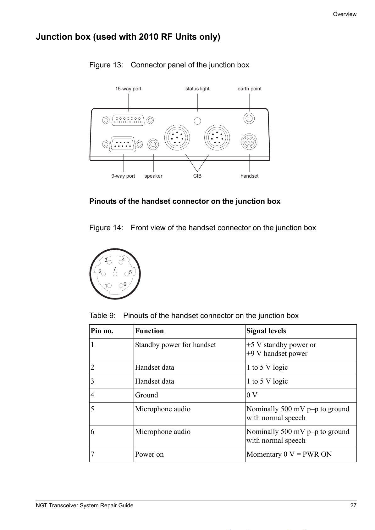
Junction box (used with 2010 RF Units only)
Figure 13: Connector panel of the junction box
Pinouts of the handset connector on the junction box
Figure 14: Front view of the handset connector on the junction box
Table 9: Pinouts of the handset connector on the junction box
Pin no. Function Signal levels
1 Standby power for handset +5 V standby power or
+9 V handset power
2 Handset data 1 to 5 V logic
3 Handset data 1 to 5 V logic
4 Ground 0 V
5 Microphone audio Nominally 500 mV p–p to ground
with normal speech
6 Microphone audio Nominally 500 mV p–p to ground
with normal speech
7 Power on Momentary 0 V = PWR ON
15-way port status light earth point
handsetCIBspeaker9-way port
1
2
3
4
5
6
7

Overview
28 NGT Transceiver System Repair Guide
Pinouts of the CIB connectors on the junction box
Figure 15: Front view of a CIB connector on the junction box
Pinouts of the speaker connector on the junction box
The speaker should be 4 Ω with a power rating of 5 W.
Table 10: Pinouts of the CIB connectors on the junction box
Pin no. Function Signal levels
1 Ground 0 V
2 System data 1 to 5 V logic
3 System data 1 to 5 V logic
4 Power on Momentary 0 V = PWR ON
5 +6 V standby +6 V
6 System audio + 5 to 10 V sync and TDM
7 System audio – 0 to 5 V sync and TDM
8 A rail protected (2 A) +13.6 V nominal
Table 11: Pinouts of the speaker connector on the junction box
Connection Function
Tip Speaker audio output
Sleeve Ground
1
2
3
4
5
6
7
8

Overview
NGT Transceiver System Repair Guide 29
Pinouts of the 9-way serial data connector on the junction box
Figure 16: Front view of the 9-way serial data connector on the junction box
Table 12: Pinouts of the 9-way serial data connector on the junction box
Pin no. Function Signal levels
1N/C
2 RS232 Receive data RS232 input
3 RS232 Transmit data RS232 output
4 DTR RS232 output
5 Ground 0 V
6 DSR RS232 input
7 RTS RS232 output
8 CTS RS232 input
9N/C
1
69
5

Overview
30 NGT Transceiver System Repair Guide
Pinouts of the 15-way GPIO connector on the junction box
Figure 17: Front view of the 15-way GPIO connector on the junction box
Table 13: Pinouts of the 15-way GPIO connector on the junction box
Pin no. Function Signal levels
1 RTS 0 to 5 V
2 RS232 Receive data RS232 input
3 RS232 Transmit data RS232 output
4 Ground 0 V
5 Tx audio input (50 kΩ balanced) 300 mV p–p ALC threshold
6 External alarm relay Contacts rated 50 V, 1 A
7 External alarm relay Closed for alarm
8 A rail +13.6 V nominal
9 CTS RS232 input
10 PTT input 5 V TTL logic active low
11 Morse input 5 V TTL logic active low
12 Spare input/output 5 V TTL logic
13 Spare input/output 5 V TTL logic
14 System audio output 1 V p–p (maximum load 1 kΩ)
15 Tx audio input (50 kΩ balanced) 300 mV p–p ALC threshold
NOTE
Pins 6, 7 and 9 may be linked internally to select normally open or closed.
The pins can be configured to switch to ground or the A rail.
1
915
8

Overview
NGT Transceiver System Repair Guide 31
Pinouts of the headphone jack on the desk console
Table 14: Pinouts of the headphone jack on the desk console
Connection Function
Ring Audio
Tip Audio
Sleeve Ground

Overview
32 NGT Transceiver System Repair Guide
This page has been left blank intentionally.

NGT Transceiver System Repair Guide 33
Brief description (2010 RF Unit with 2030 Junction Box)
This section contains the following topics:
General information (35)
Transmit path (36)
Receive path (39)
Synthesiser operation (40)
Control and switching (40)

Brief description (2010 RF Unit with 2030 Junction Box)
34 NGT Transceiver System Repair Guide
This page has been left blank intentionally.

03-01032 Issue 2

03-01032 Issue 4

Brief description (2010 RF Unit with 2030 Junction Box)
NGT Transceiver System Repair Guide 35
General information
The information in this section should be read in conjunction with the appropriate issue
of the block diagram for the NGT series Transceiver. See below to determine which issue
of the block diagram you should be viewing.
For transceivers with:
The transceiver uses double conversion in both the Receive and Transmit modes. Only
the 455 kHz sideband filter and the local oscillators VCO and REF OSC are common to
both modes of operation.
The signal routing is determined by switching and control voltages according to the
selected mode.
Codan part number of PCB assembly See...
Audio PCB (2030 Junction Box) 03-01032 Issue 2
08-05470
Application Processor PCB (2010 RF Unit)
08-05265
RF/IF PCB (2010 RF Unit)
08-05261
PA PCB (2010 RF Unit)
08-05415
08-05416
08-05511
Audio PCB (2030 Junction Box) 03-01032 Issue 4
08-05986
RF/IF PCB (2010 RF Unit)
08-05889
PA PCB (2010 RF Unit)
08-05869 or 08-06461
08-05910

Brief description (2010 RF Unit with 2030 Junction Box)
36 NGT Transceiver System Repair Guide
Transmit path
Handset transmit path
The microphone audio is amplified in the handset and passed to the junction box via the
handset bus.
Junction box transmit path
The audio from the handset is amplified and gated to produce TDM channel audio on the
Audio PCB in the junction box. There are eight time slots for the TDM, comprising one
synchronisation channel and seven audio channels.
The audio is passed to the RF unit via the CIB.
Time division multiplex audio channels
The system audio uses TDM to produce seven channels of audio and one
synchronisation pulse to reference the channel timing to pass audio between the RF unit
and the junction box(es).
The audio is sampled at a rate of 12.5 kHz by the TDM gates. The position of the audio
channel varies depending on the requirements of the system.
Figure 18: Representation of the waveform
The TDM audio is passed via SYS AUDIO+/– on the CIB.
Sync pulse
Time
Audio (channel 3)
Channels

Brief description (2010 RF Unit with 2030 Junction Box)
NGT Transceiver System Repair Guide 37
CIB transmit path
The CIB is an 8-wire bus that connects all the units in the system together:
• SYS AUDIO+/–: The audio is TDM balanced, as described on page 36, Time
division multiplex audio channels.
• SYS DATA+/–: The data uses CAN protocol. This protocol has good error detection
capabilities and performs well in high-noise environments. The data rate on the CIB
is 125 kbps.
• STBY: Standby power is a 100 mA, 6 V DC continuous supply. This is used to
backlight the key at night.
• A PROTECTED: The Protected A rail is an unregulated supply that is used to
supply power to all the units in the transceiver system. The maximum current that
this can supply is 2 A. If very long runs of the CIB cabling are required, an external
supply may be connected to the junction box to supply power locally.
• PWR ON: The power on line is used to switch the transceiver on when the line is
grounded.
• GND: Ground is the supply return wire and is connected to the negative terminal of
the battery.
RF unit transmit path
Audio Interface PCB
The audio from the junction box connects to the Audio Interface PCB. This PCB
decodes the TDM audio to normal audio.
Application Processor PCB
The transmit audio is passed to the Application Processor PCB for compression, which
converts the signal to a fixed level before passing to the RF/IF PCB.
RF/IF PCB
The audio is mixed with the local oscillator to produce double sideband. It is then filtered
by a 2.5 kHz sideband filter centred on 455 kHz, so that only the wanted sideband is
passed to the first mixer. It is then mixed with the reference oscillator to produce an IF
signal centred on 45 MHz.
The transmit signal is filtered by a BPF with a bandwidth of 15 kHz, before being passed
to the input of the second mixer.
At the second mixer, the signal mixes with the local oscillator VCO to produce the
required channel frequency. The signal is passed to the PA PCB.

Brief description (2010 RF Unit with 2030 Junction Box)
38 NGT Transceiver System Repair Guide
PA PCB
On the PA PCB, the signal is amplified then passed through the transmit/receive relay to
the selected LPF.
The output from the LPF is passed via the VSWR detector to the RF output connector.
From there it is connected by coaxial cable to the antenna.

Brief description (2010 RF Unit with 2030 Junction Box)
NGT Transceiver System Repair Guide 39
Receive path
RF unit receive path
PA PCB
The receive signal from the antenna passes through a PA LPF to the transmit/receive
relay. It is then passed to the receiver input on the RF/IF PCB.
RF/IF PCB
From the receiver input, the signal passes to the input of the first balanced mixer. Here it
mixes with the local oscillator VCO to produce an IF signal centred on 45 MHz.
The 45 MHz signal is filtered using a BPF with a bandwidth of 15 kHz, before being
passed to the second balanced mixer. The signal mixes with 44.545 MHz to produce an
IF signal centred on 455 kHz.
The output from the second mixer passes through a 2.5 kHz sideband filter so that only
the wanted sideband is fed to the high-gain AGC IF amplifier.
The amplified 455 kHz signal is demodulated to produce an audio signal and also to
operate an AGC circuit. This circuit controls the gain of the IF amplifier to prevent
overloading when strong signals are received. It also maintains constant audio output
with changing input signals.
Audio Interface PCB
The audio is passed to the Audio Interface PCB where it divides into two paths. One path
is the unprocessed (raw) audio on one TDM channel. The other path is passed to the
Application Processor PCB where the audio is enhanced (noise-reduced). This audio is
then passed back to the Audio Interface PCB and becomes another TDM audio channel.
The audio is then passed to the junction box via the CIB.
Junction box receive path
The audio from the RF unit is decoded and either raw audio or noise-reduced audio (as
selected by the user) is passed to the speaker.

Brief description (2010 RF Unit with 2030 Junction Box)
40 NGT Transceiver System Repair Guide
Synthesiser operation
The transceiver uses a single loop synthesiser. The synthesiser VCO is used as the first
mixer LO, generating an oscillator frequency in 10 Hz steps. In Receive mode, the
frequency of the oscillator ranges from 45.25 MHz to 75 MHz. In Transmit mode, the
frequency of the oscillator ranges from 46.6 MHz to 75 MHz.
The reference oscillator (REF OSC) at 44.545 MHz is used as the second mixer LO. This
frequency is also fed to two DDS ICs to produce a variable reference frequency for VCO
with 10 Hz resolution.
The second DDS IC produces 456.5 kHz (USB) and 453.5 kHz (LSB) for the Tx MOD
and Rx DEMOD circuits.
The reference oscillator at 14.848333 MHz is fed through a 44.5 MHz BPF to select the
3rd harmonic to produce the 44.545 MHz second mixer LO. The 14.848333 MHz
frequency is also fed to two DDS ICs to produce a variable reference frequency for VCO
with 10 Hz resolution.
The second DDS IC produces 456.5 kHz (USB) and 453.5 kHz (LSB) for the Tx MOD
and Rx DEMOD circuits.
Control and switching
Most functions of the transceiver are controlled by microprocessors.
A microprocessor in the handset reads the key strokes entered by the user. The keyed
data is then passed to the junction box via the handset bus. The junction box sends data
to the handset to update the display.
A microprocessor in the junction box transmits commands and data onto the CIB using
the CAN protocol. The data rate on the bus is 125 kbps.
The RF unit receives the data, decodes it and then carries out the required function.
The RF unit contains five microprocessors located on four PCBs. Incoming data first
goes to the main application microprocessor. This microprocessor then commands lower
level microprocessors to carry out the required function.
ALTERNATIVE TEXT
ALTERNATIVE TEXT

NGT Transceiver System Repair Guide 41
Brief description (2011/2012 RF Unit)
This section contains the following topics:
General information (43)
Transmit path (44)
Receive path (45)
Synthesiser operation (46)
Control and switching (46)

Brief description (2011/2012 RF Unit)
42 NGT Transceiver System Repair Guide
This page has been left blank intentionally.

03-01126

03-01190

Brief description (2011/2012 RF Unit)
NGT Transceiver System Repair Guide 43
General information
The transceiver uses double conversion in both the Receive and Transmit modes. Only
the 455 kHz sideband filter and the local oscillators VCO and REF OSC are common to
both modes of operation.
The signal routing is determined by switching and control voltages according to the
selected mode.
NOTE
The information in this section should be read in conjunction with the
appropriate block diagram for the RF unit. See below to determine which
block diagram you should be viewing.
For RF unit type... See...
2011 03-01126
2012 03-01190

Brief description (2011/2012 RF Unit)
44 NGT Transceiver System Repair Guide
Transmit path
Handset transmit path
The microphone audio is amplified in the handset and passed to the RF unit via the
handset and speaker connection cable.
RF unit transmit path
2011—Audio & Interconnect PCB
The audio from the microphone is buffered on the Audio & Interconnect PCB, then
passed to the Application Processor Handset I/F 3 V PCB for compression to convert the
signal to a fixed level. This signal is then returned to the Audio & Interconnect PCB
where it is forwarded to the RF/IF PCB.
2012—Audio Interconnect & Data I/O PCB
The audio from the microphone is buffered on the Audio Interconnect & Data I/O PCB,
then passed to the Application Processor Handset & Data I/F PCB for compression to
convert the signal to a fixed level. This signal is then returned to the Audio Interconnect
& Data I/O PCB where it is forwarded to the RF/IF PCB.
RF/IF PCB
The audio is mixed with the local oscillator to produce double sideband. It is then filtered
by a 2.5 kHz sideband filter centred on 455 kHz, so that only the wanted sideband is
passed to the first mixer. It is then mixed with the reference oscillator to produce an IF
signal centred on 45 MHz.
The transmit signal is filtered by a BPF with a bandwidth of 15 kHz, before being passed
to the input of the second mixer.
At the second mixer, the signal mixes with the local oscillator VCO to produce the
required channel frequency. The signal is passed to the PA PCB.
PA PCB
On the PA PCB, the signal is amplified then passed through the transmit/receive relay to
the selected LPF.
The output from the LPF is passed via the VSWR detector to the RF output connector.
From there it is connected by coaxial cable to the antenna.

Brief description (2011/2012 RF Unit)
NGT Transceiver System Repair Guide 45
Receive path
RF unit receive path
PA PCB
The receive signal from the antenna passes through a PA LPF to the transmit/receive
relay. It is then passed to the receiver input on the RF/IF PCB.
RF/IF PCB
From the receiver input, the signal passes via a selectable pre-amplifier to the input of the
first balanced mixer. Here it mixes with the local oscillator VCO to produce an IF signal
centred on 45 MHz.
The 45 MHz signal is filtered using a BPF with a bandwidth of 15 kHz, before being
passed to the second balanced mixer. The signal mixes with 44.545 MHz to produce an
IF signal centred on 455 kHz.
The output from the second mixer passes through a 2.5 kHz sideband filter so that only
the wanted sideband is fed to the high-gain AGC IF amplifier.
The amplified 455 kHz signal is demodulated to produce an audio signal and also to
operate an AGC circuit. This circuit controls the gain of the IF amplifier to prevent
overloading when strong signals are received. It also maintains constant audio output
with changing input levels.
2011—Audio & Interconnect PCB
The audio is passed to the Audio & Interconnect PCB where it divides into two paths.
One path is the unprocessed (raw) audio. The other path is passed to the Application
Processor Handset I/F 3 V PCB where the audio is enhanced (noise-reduced) before
returning to the Audio & Interconnect PCB. The required audio path is switch-selected
and passed to the audio amplifier, then to the speaker via the handset and speaker
connection cable.
2012—Audio Interconnect & Data I/O PCB
The audio is passed to the Audio Interconnect & Data I/O PCB where it divides into two
paths. One path is the unprocessed (raw) audio. The other path is passed to the
Application Processor Handset & Data I/F PCB where the audio is enhanced (noise-
reduced) before returning to the Audio Interconnect & Data I/O PCB. The required audio
path is switch-selected and passed to the audio amplifier, then to the speaker via the
handset and speaker connection cable.

Brief description (2011/2012 RF Unit)
46 NGT Transceiver System Repair Guide
Synthesiser operation
The transceiver uses a single loop synthesiser. The synthesiser VCO is used as the first
mixer LO, generating an oscillator frequency in 10 Hz steps. In Receive mode, the
frequency of the oscillator ranges from 45.25 MHz to 75 MHz. In Transmit mode, the
frequency of the oscillator ranges from 46.6 MHz to 75 MHz.
The reference oscillator at 14.848333 MHz is fed through a 44.5 MHz BPF to select the
3rd harmonic to produce the 44.545 MHz second mixer LO. The 14.848333 MHz
frequency is also fed to two DDS ICs to produce a variable reference frequency for VCO
with 10 Hz resolution.
The second DDS IC produces 456.5 kHz (USB) and 453.5 kHz (LSB) for the Tx MOD
and Rx DEMOD circuits.
Control and switching
Most functions of the transceiver are controlled by microprocessors.
A microprocessor in the handset reads the key strokes entered by the user. The keyed
data is then passed to the RF unit via the differential handset bus. The RF unit sends data
to the handset to update the display over the same bus.
The RF unit contains five microprocessors located on four PCBs. Incoming data first
goes to the main application microprocessor. This microprocessor then commands lower
level microprocessors to carry out the required function.

NGT Transceiver System Repair Guide 47
Interconnection diagrams and listed spares drawings
The drawings listed in this section are required during repair of an NGT series
Transceiver.
Table 15: List of drawings
Title Drawing number
Interconnection Diagram
2010 04-03223
2030 04-03562
2011 04-03437
2012 04-03533
Handset—NGT Listed Spares 16-00111-001 (sheet 1)
Desktop Console—NGT Listed Spares 16-00111-002 (sheet 1)
Junction Box—NGT Listed Spares 16-00111-003 (sheet 1)
RF Unit—NGT Listed Spares 16-00111-004 (sheet 1)
16-00111-004 (sheet 2)
RF Unit—NGT Listed Spares MS1253 16-00114 (sheet 1)
16-00114 (sheet 2)

Interconnection diagrams and listed spares drawings
48 NGT Transceiver System Repair Guide
This page has been left blank intentionally.

04-03223

04-03562
CODAN

04-03437

04-03533

16-00111-001 (sheet 1)

16-00111-002 (sheet 1)

16-00111-003 (sheet 1)
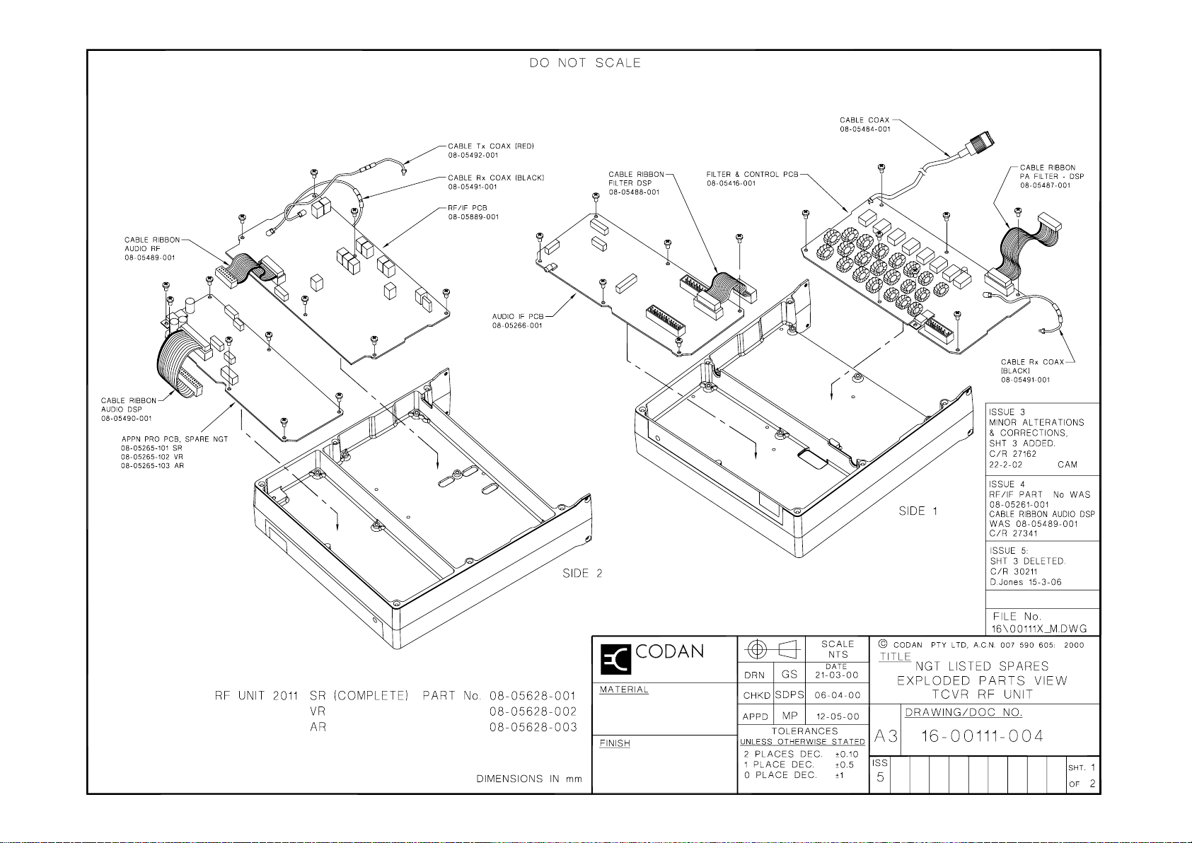
16-00111-004 (sheet 1)

16-00111-004 (sheet 2)

16-00114 (sheet 1)

16-00114 (sheet 2)
NGT Transceiver System Repair Guide 49
Functional description of PCBs
This section contains the following topics:
Handset (61)
Junction box (used with 2010 RF Units only) (63)
RF unit (68)
NOTE
The functional description should be read in conjunction with the
appropriate brief description (see page 33, Brief description (2010 RF
Unit with 2030 Junction Box) or page 41, Brief description (2011/2012
RF Unit)).

Functional description of PCBs
50 NGT Transceiver System Repair Guide
This page has been left blank intentionally.

This page has been left blank intentionally.
Functional description of PCBs
NGT Transceiver System Repair Guide 51

Functional description of PCBs
Figure 19: Handset PCB (08-05300-001)
Figure 21: Audio PCB (08-05986-001)
Figure 20: Audio PCB (08-05470-001)
Figure 22: Microprocessor PCB (08-05317-001)
52 NGT Transceiver System Repair Guide

This page has been left blank intentionally.
Functional description of PCBs
NGT Transceiver System Repair Guide 53

Functional description of PCBs
Figure 23: Audio Interface PCB (08-05266-001)
Figure 25: Audio Interconnect & Data I/O PCB (08-06261-001)
Figure 24: Audio & Interconnect PCB (08-05988-001)
Figure 26: Application Processor PCB (08-05265-001)
54 NGT Transceiver System Repair Guide

This page has been left blank intentionally.
Functional description of PCBs
NGT Transceiver System Repair Guide 55

Functional description of PCBs
Figure 27: Application Processor Handset I/F 3 V PCB (08-05987-001)
Figure 29: RF/IF PCB (08-05261-001)
Figure 28: Application Processor Handset & Data I/F PCB (08-06260-001)
Figure 30: RF/IF PCB (08-05889-001)
56 NGT Transceiver System Repair Guide

This page has been left blank intentionally.
Functional description of PCBs
NGT Transceiver System Repair Guide 57

Functional description of PCBs
Figure 31: PA PCB (08-05415-001)
Figure 33: PA PCB (08-05869-001)
Figure 32: PA PCB (08-05511-001)
Figure 34: PA PCB (08-06461-001)
58 NGT Transceiver System Repair Guide

This page has been left blank intentionally.
Functional description of PCBs
NGT Transceiver System Repair Guide 59

Functional description of PCBs
Figure 35: Filter and Control PCB (08-05416-001)
Figure 36: Filter and Control PCB (08-05910-001)
60 NGT Transceiver System Repair Guide

Functional description of PCBs
NGT Transceiver System Repair Guide 61
Handset
Handset PCB
The Handset PCB performs the following functions:
• interprets data from the Microprocessor PCB (junction box)/Audio &
Interconnect PCB (2011)/Audio Interconnect & Data I/O PCB (2012) and displays it
on the handset screen
• reads keypad entries and sends data to the Microprocessor PCB (junction
box)/Audio & Interconnect PCB (2011)/Audio Interconnect & Data I/O PCB (2012)
• provides an RS232 port for programming
• provides some pre-amplification of microphone audio
• provides brightness and contrast adjustment for LCD
The Handset PCB contains:
• a microprocessor with ROM and RAM (IC1)
• an LCD and drivers (H1)
• a connection to the keypad matrix
• a programming port (J1)
• an I/O IC to drive the handset bus (IC8)
• a microphone amplifier (IC9)
For details on the Handset PCB,
Codan part number
See...
08-05300-001 Table 16 on page 62 and
Figure 19 on page 52

Functional description of PCBs
62 NGT Transceiver System Repair Guide
08-05300-001
CAUTION
If this PCB is replaced, ensure that IC3 has the same (or later) firmware
version as the original.
Table 16: Test points for the Handset PCB (08-05300-001)
Test point Correct signal Explanation
+5V 5.0 V 5 V supply rail regulated on-board. This supplies power for the
display driver microcontroller, the display, the RS232 serial
port driver and the handset data driver.
+9V 9.0 V 9 V nominal supply rail. Only present when the transceiver is
switched on. This supplies the microphone pre-amp, display
and handset backlighting, and the RS232 serial port driver.
VEE –0.8 V to –2.4 V LCD contrast control voltage. Typically, this measures –1.3 V,
depending on the contrast setting. The negative voltage is
generated by the RS232 driver IC.
Pin 1, P8 5.4 V
9.2 V
5.4 V when the transceiver is switched off. Power is supplied
from the Audio PCB (junction box)/Audio & Interconnect PCB
(2011)/Audio Interconnect & Data I/O PCB (2012).
9.2 V when the transceiver is switched on.
Pin 6 & 7, P8 500 mV p–p Push-pull balanced amplified microphone audio.
Pin 8, P8 12.9 V
0.4 V
12.9 V when the transceiver is switched off. Power is supplied
from the Audio PCB (junction box)/Audio & Interconnect PCB
(2011)/Audio Interconnect & Data I/O PCB (2012).
0.4 V when the transceiver is switched on.

Functional description of PCBs
NGT Transceiver System Repair Guide 63
Junction box (used with 2010 RF Units only)
Audio PCB
The Audio PCB performs the following functions:
• provides amplification and volume control for speaker audio
• provides level control of beeps
• provides level control of morse tone
• provides level control of external Tx audio input (GPIO source)
• controls TDM audio sampling gates
• provides external port connections for Tx audio input, Rx audio output, PTT, and
RS232 (GPIO port)
• provides external alarm relay contacts (GPIO port)
• provides connection point for desk console
The Audio PCB contains:
• an audio amplifier (IC3)
• digital volume control elements
• Rx and Tx audio active filters
• an EPLD to control the TDM switching
For details on the Audio PCB,
Codan part number
See...
08-05470-001 Table 17 on page 64 and
Figure 20 on page 52
08-05986-001 Table 18 on page 65 and
Figure 21 on page 52

Functional description of PCBs
64 NGT Transceiver System Repair Guide
08-05470-001
CAUTION
If this PCB is replaced, ensure that IC1 has the same (or later) firmware
version as the original.
Table 17: Test points for the Audio PCB (08-05470-001)
Test point Correct signal Explanation
+5V 5.0 V 5 V supply rail regulated on-board.
+10V 10.0 V 10 V supply rail regulated on-board.
Pin 9 & 10, P3 13.6 V 13.6 V supplied from the RF unit via the CIB cable.
Pin 1, P7 5.4 V
9.2 V
5.4 V when the transceiver is switched off. Power is supplied to
the handset.
9.2 V when the transceiver is switched on.
TX_AF 1 V p–p audio Filtered and level-controlled Tx audio prior to being
multiplexed onto the CIB.
RX_AF 600 mV p–p audio Filtered and level-controlled Rx audio before being applied to
the volume control circuitry.
AUDIO_O/P High level audio Rx audio output as applied to the speaker. This can be as high as
12 V p–p at the onset of clipping, depending on the volume
level.
Pin 12, P10 1 V p–p Audio output to GPIO.
TP1
TP2
TDM audio On the CRO, this waveform should appear as 5 V p–p
amplitude (10 V p–p differential) 10 µs-wide sync pulses,
followed by seven channels of sampled audio of approximately
1 V p–p (2 V p–p differential) amplitude. TDM slot 1 typically
carries Rx audio, slot 2 carries enhanced Rx audio, and slot 3
carries Tx audio.
TP3
TP4
CAN DATA High
CAN DATA Low
CAN digital serial data stream. CAN in the NGT operates at
125 kbps. CAN High and CAN Low form a differential pair.
CAN High nominally measures 3.80 V with approx. 3 V
amplitude low-going pulses, and CAN Low nominally
measures 1.4 V with approx. 3 V amplitude high-going pulses.

Functional description of PCBs
NGT Transceiver System Repair Guide 65
08-05986-001
CAUTION
If this PCB is replaced, ensure that IC1 has the same (or later) firmware
version as the original.
Table 18: Test points for the Audio PCB (08-05986-001)
Test point Correct signal Explanation
+3V3 3.3 V 3.3 V supply rail regulated on-board.
+5V 5.0 V 5 V supply rail regulated on-board.
+10V 10.0 V 10 V supply rail regulated on-board.
Pin 9 & 10, P3 13.6 V 13.6 V supplied from the RF unit via the CIB cable.
Pin 1, P7 5.4 V
9.2 V
5.4 V when the transceiver is switched off. Power is supplied to
the handset.
9.2 V when the transceiver is switched on.
TX_AF 1 V p–p audio Filtered and level-controlled Tx audio prior to being
multiplexed onto the CIB.
RX_AF 1 V p–p audio Filtered and level-controlled Rx audio before being applied to
the volume control circuitry.
AUDIO_O/P High level audio Rx audio output as applied to the speaker. This can be as high as
12 V p–p at the onset of clipping, depending on the volume
level.
Pin 12, P10 1 V p–p Audio output to GPIO.
TP1
TP2
TDM audio On the CRO, this waveform should appear as 5 V p–p
amplitude (10 V p–p differential) 10 µs-wide sync pulses,
followed by seven channels of sampled audio of approximately
1 V p–p (2 V p–p differential) amplitude. TDM slot 1 typically
carries Rx audio, slot 2 carries enhanced Rx audio, and slot 3
carries Tx audio.
TP3
TP4
CAN DATA High
CAN DATA Low
CAN digital serial data stream. CAN in the NGT operates at
125 kbps. CAN High and CAN Low form a differential pair.
CAN High nominally measures 3.80 V with approx. 3 V
amplitude low-going pulses, and CAN Low nominally
measures 1.4 V with approx. 3 V amplitude high-going pulses.

Functional description of PCBs
66 NGT Transceiver System Repair Guide
Microprocessor PCB
The Microprocessor PCB performs the following functions:
• generates local speaker beeps and morse code tones when required
• sends and receives commands from the handset
• sends and receives commands from the RF unit via the CIB
• stores user data: Address List, Phone Link List, Keypad List, junction box control
macros
• controls arbitration of the system audio bus
The Microprocessor PCB contains:
• a microprocessor (IC1)
• a static RAM (IC8)
• a program flash ROM (IC4)
• a CAN controller (IC11)
• a CAN I/O IC
• a UART and RS232 I/O driver IC
• a tone generator
• an I/O data driver for handset bus
• the TPE and Service mode links
For details on the Microprocessor PCB,
Codan part number
See...
08-05317-001 Table 19 on page 67 and
Figure 22 on page 52

Functional description of PCBs
NGT Transceiver System Repair Guide 67
08-05317-001
CAUTION
If this PCB is replaced, ensure that IC4 has the same (or later) firmware
version as the original.
Table 19: Test points for the Microprocessor PCB (08-05317-001)
Test point Correct signal Explanation
+3V3 3.3 V 3.3 V supply rail regulated on-board.
Pin 1, IC13 5.0 V 5 V supply rail regulated on-board.
Pin 17 & 18, X1 13.6 V 13.6 V supplied from the Audio PCB.
Pin 4, IC7 16 MHz square
wave
Buffered version of the clock to the microprocessor IC1.
Absence of this clock signal means IC1 is not running correctly.
Z2 3.6864 MHz Clock for IC10.

Functional description of PCBs
68 NGT Transceiver System Repair Guide
RF unit
Audio Interface PCB (2010 RF Unit only)
The Audio Interface PCB performs the following functions:
• converts balanced CIB audio into single-ended Tx and Rx audio
• indicates to the Application Processor PCB to mute the audio output when an Rx
signal is not present
• provides a mute detector circuit with logic level output for the Application
Processor PCB
• converts balanced CIB data into single-ended TTL data stream
• provides routing of Tx audio to the RF/IF PCB
• decodes and encodes TDM system audio
• generates sync timing pulses for the TDM system audio
• provides power on/off function; switches volts to the power relay on the Filter and
Control PCB
• provides battery-backed real time clock
• provides current-limited, overload-protected, battery DC supply to the CIB
The Audio Interface PCB contains:
• a PIC microprocessor (IC12)
• an EPLD (IC11)
• a CAN I/O IC
• TDM sampling gates
• a mute detector circuit
• a fuse that may be reset electronically (IC14)
For details on the Audio Interface PCB,
Codan part number
See...
08-05266-001 Table 20 on page 69 and
Figure 23 on page 54

Functional description of PCBs
NGT Transceiver System Repair Guide 69
08-05266-001
CAUTION
If this PCB is replaced, ensure that IC11 and IC12 have the same (or later)
firmware versions as the originals.
Table 20: Test points for the Audio Interface PCB (08-05266-001)
Test Point Correct Signal Explanation
+5V 5.0 V 5 V supply rail regulated on-board.
+10V 10.0 V 10 V supply rail regulated on-board.
A 13.6 V 13.6 V supplied from the Filter and Control PCB.
A PROT 13.6 V Protected power supply voltage. It is supplied to the CIB and
the antenna control cable. It is current limited and short-circuit
protected.
Pin 5, P1 13 V
0.4 V
13 V when the transceiver is switched off.
0.4 V when the transceiver is switched on. Switched in the
handset.
+6V_STBY 6.2 V Standby power for the handset supplied via the CIB and the
junction box.
RESET 5.0 V Resets microprocessors when low.
RX_AUDIO 800 mV p–p Rx audio supplied from the RF/IF PCB.
TX_AUDIO1 700 mV p–p Tx audio supplied to the Application Processor PCB for digital
enhancing.
TX_AUDIO2 1 V p–p Digitally enhanced Tx audio supplied to the RF/IF PCB.
MUTE
5V
0V
Mute detect.
5 V when a signal is present.
0 V when no signal is present.
SYNC_ERR 0 V TDM audio synchronisation error status.
MASTER_MODE 5.0 V TDM master indicator. This shows which RF unit is generating
the TDM synchronisation pulses when multiple RF units are
present on one bus. In the test configuration, this should be
5.0 V.
SYS_AUDIO1
SYS_AUDIO2
TDM audio On the CRO, this waveform should appear as 5 V p–p
amplitude (10 V p–p differential) 10 µs-wide sync pulses,
followed by seven channels of sampled audio of approximately
1 V p–p (2 V p–p differential) amplitude. TDM slot 1 typically
carries Rx audio, slot 2 carries enhanced Rx audio, and slot 3
carries Tx audio.
 Loading...