

Page 1

GR716-MINI
Development Board
2019 User's Manual
The most important thing we build is trust
GR716-MINI
Development Board
User's Manual
GR716-MINI-UM, 2019, Version 0.2 www.cobham.com/gaisler
Page 2

GR716-MINI
Intentionally Blank
GR716-MINI-UM, May 2019, Version 0.2 2 www.cobham.com/gaisler
Page 3

GR716-MINI
Table of Contents
1 Introduction......................................................................................................................5
1.1 Scope of the Document.......................................................................................5
1.2 Reference Documents..........................................................................................5
2 Abbreviations...................................................................................................................6
3 Introduction......................................................................................................................7
3.1 Overview.............................................................................................................7
3.2 Handling..............................................................................................................8
4 Board Design....................................................................................................................9
4.1 Board Block Diagram..........................................................................................9
4.2 Board Mechanical Configuration......................................................................10
4.3 GR716 Microcontroller.....................................................................................12
4.4 Memory.............................................................................................................13
4.5 Expansion/Interface Connector.........................................................................14
4.6 LVDS Interfaces................................................................................................15
4.7 FTDI Serial to USB Interface............................................................................15
4.8 Analog Signals...................................................................................................16
4.9 GPIO..................................................................................................................17
4.10 Bootstrap Signals...............................................................................................18
4.11 Debug Support Unit Interfaces..........................................................................19
4.12 Oscillators and Clock Inputs.............................................................................20
4.13 Power Supply and Voltage Regulation..............................................................21
4.14 Reset Circuit and Button...................................................................................22
4.15 Watchdog...........................................................................................................22
5 Setting Up and Using the Board...................................................................................23
6 Interfaces and Configuration.......................................................................................24
6.1 List of Connectors.............................................................................................24
6.2 List of Oscillators, Switches and LED's............................................................26
7 Change Record...............................................................................................................29
GR716-MINI-UM, May 2019, Version 0.2 3 www.cobham.com/gaisler
Page 4

GR716-MINI
List of Figures
Figure 3-1: GR716-MINI Development Board....................................................................................7
Figure 4-1: GR716-MINI Board Block Diagram.................................................................................9
Figure .4-2: GR716-MINI Board Dimensions (top side)...................................................................10
Figure .4-3: GR716-MINI Board Dimensions (bottom side - expansion connector).........................10
Figure 4-4: Example of a Carrier board..............................................................................................11
Figure 4-5: GR716 Microcontroller Block Diagram..........................................................................12
Figure 4-6: GR716 Package...............................................................................................................12
Figure 4-7: SPI Boot Memory Connections.......................................................................................13
Figure 4-8: SRAM Signal Connections..............................................................................................13
Figure 4-9: Expansion/Interface Connector.......................................................................................14
Figure 4-10: Block diagram of FTDI Serial to USB Interface...........................................................15
Figure 4-11: MMCX analog connector interface...............................................................................16
Figure 4-12: Debug Support Unit connections...................................................................................19
Figure 4-13: Board level Clock Distribution Scheme........................................................................20
Figure 4-14: Power Regulation Scheme.............................................................................................21
Figure 6-1: PCB Top View.................................................................................................................27
Figure 6-2: PCB Bottom View...........................................................................................................27
Figure 6-3: PCB Top View (Photo)....................................................................................................28
Figure 6-4: PCB Bottom View (Photo)..............................................................................................28
List of Tables
Table 1: List of Expansion Connector signals....................................................................................14
Table 2: FTDI USB-Serial Port Assignment......................................................................................15
Table 3: List of GPIO pins connected to Expansion Connector.........................................................17
Table 4: Bootstrap Resistor Settings...................................................................................................18
Table 5: Default Setting of Jumpers...................................................................................................23
Table 6: List of Connectors................................................................................................................24
Table 7: J1 USB type Micro B connector – FTDI Serial Link...........................................................24
Table 8: J2,J3,J4,J5 MMCX miniature coax connectors....................................................................24
Table 9: Expansion connector P1 Pin-out...........................................................................................25
Table 10: List and definition of Oscillators and Crystals...................................................................26
Table 11: List and definition of PCB mounted LED's........................................................................26
Table 12: List and definition of Switches...........................................................................................26
GR716-MINI-UM, May 2019, Version 0.2 4 www.cobham.com/gaisler
Page 5

GR716-MINI
1 Introduction
1.1 Scope of the Document
This document provides a User's Manual and Interface document for the “GR716MINI” Development and Demonstration board.
The work has been performed by Cobham Gaisler AB, Göteborg, Sweden.
1.2 Reference Documents
[RD1] GR716, Data Sheet and User's Manual",Cobham Gaisler, GR716-UM-DS, available
from http://www.gaisler.com/index.php/products/components/GR716
[RD2] GR716-MINI_schematic.pdf, Schematic
[RD3] GR716-MINI_assy_drawing.pdf, Assembly Drawing
[RD4] GRMON3 User's Manual, available from:
https://www.gaisler.com/index.php/products/debug-tools/grmon3
GR716-MINI-UM, May 2019, Version 0.2 5 www.cobham.com/gaisler
Page 6

GR716-MINI
2 Abbreviations
ASIC Application Specific Integrated Circuit.
DSU Debug Support Unit
EDAC Error Detection and Correction
ESA European Space Agency
ESD Electro-Static Discharge
ESTEC European Space Research and Technology Center
GPIO General Purpose Input / Output
IC Integrated Circuit
I/O Input/Output
IP Intellectual Property
LDO Low Drop-Out
PCB Printed Circuit Board
POL Point of Load
SOC System On a Chip
SPW Spacewire
TBC To Be Confirmed
TBD To Be Defined
GR716-MINI-UM, May 2019, Version 0.2 6 www.cobham.com/gaisler
Page 7
GR716-MINI
3 Introduction
3.1 Overview
This document describes the GR716-MINI Development Board.
This equipment is intended to be used as a platform for the demonstration of the
Cobham Gaisler GR716 RAD Hard Microcontroller.
Furthermore, this board provides developers with a convenient hardware platform for
the evaluation and development of software for the GR716 microcontroller.
The GR716 Microcontroller features a fault-tolerant LEON3 SPARC V8 processor,
communication interfaces and on-chip ADC, DAC, Power-on-Reset, Oscillator, Brownout detection, LVDS transceivers, regulators to support for single 3.3V supply, ideally
suited for space and other high-rel applications.
Because not all features of the GR716 can be simultaneously operated, the GR716-MINI
Development Board comprises a custom designed PCB providing a compact
implementation with a representative array of interfaces and features.
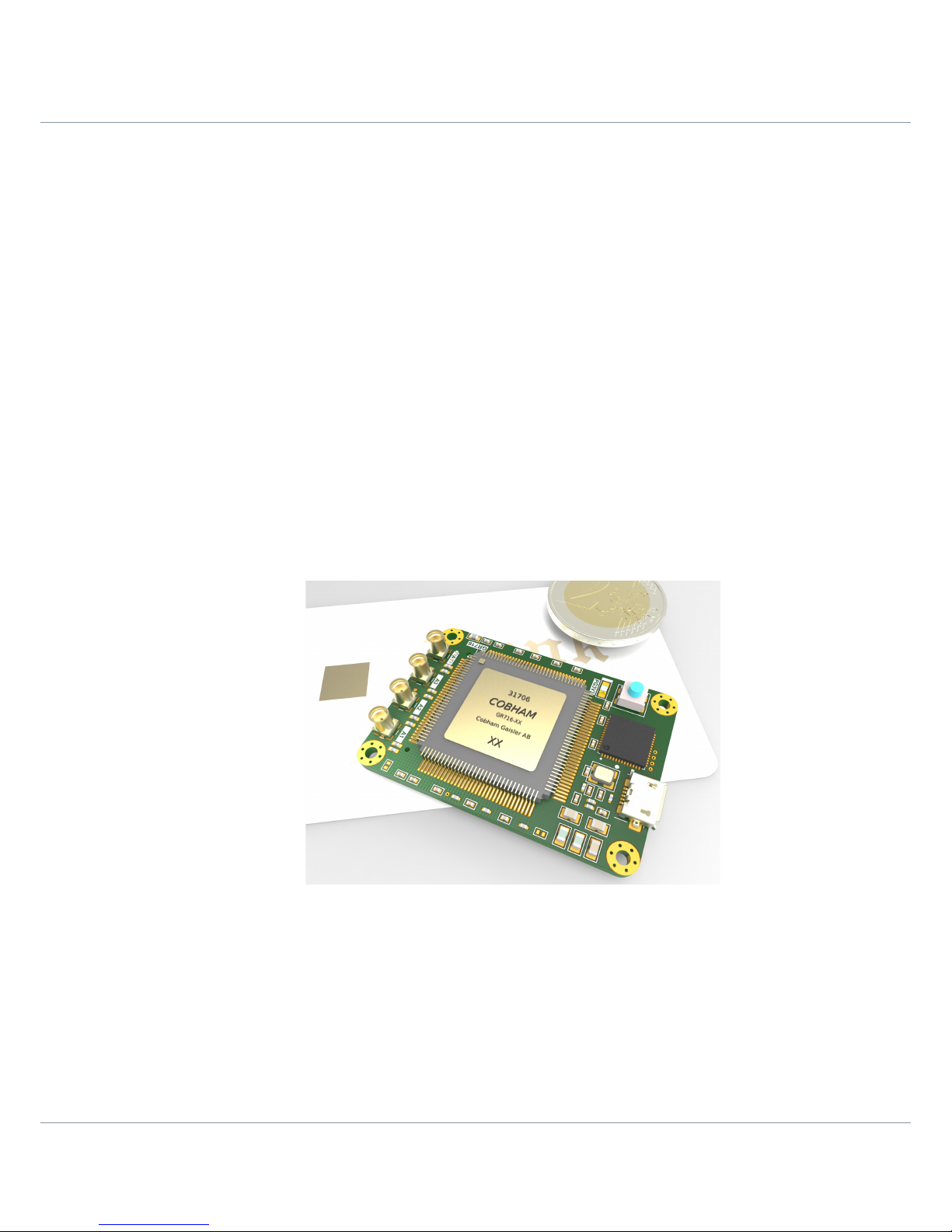
The board contains the following main items as detailed in section 4 of this document:
• size 35 x 50mm
• USB interface via FTDI FT4232 providing DSU plus 2 x UART
• on-board regulator converting from USB 5V to 3.3V.
• 16 Mbit SRAM (Cypress CY7C1069G in BGA package)
GR716-MINI-UM, May 2019, Version 0.2 7 www.cobham.com/gaisler
Figure 3-1: GR716-MINI Development Board
Page 8
GR716-MINI
• 256 Mbit SPI flash (MX25L25635FZ2I-10G in 8 pin WSON package)
• On board crystal (25MHz TBC)
• 4 x MMCX coax connectors for 4x ADC or 4x DAC (or combination)
• Miniature 80 pin Expansion connector (bottom side) with connections for
◦ Reset_IN & Reset_OUT
◦ External SPW and SYS clocks
◦ Vref_Buf_out
◦ 3 x LVDS RX + 3 x LVDS TX pairs
◦ Analog 4 x DAC + 8 x ADC (or use as standard 12 x GPIO)
◦ 13 GPIO
Debug interface support is demonstrated on the board with support for debugging via
the following interface:
• DSU-UART via FTDI USB interface
3.2 Handling
ATTENTION: OBSERVE PRECAUTIONS FOR
HANDLING ELECTROSTATIC SENSITIVE DEVICES
This unit contains sensitive electronic components which can be damaged by
Electrostatic Discharges (ESD). When handling or installing the unit observe
appropriate precautions and ESD safe practices.
When not in use, store the unit in an electrostatic protective container or bag.
When configuring the jumpers on the board, or connecting/disconnecting cables, ensure
that the unit is in an un-powered state.
When operating the board in a 'stand-alone' configuration, the power supply should be
current limited to prevent damage to the board or power supply in the event of an overcurrent situation.
This board is intended for commercial use and evaluation in a standard laboratory
environment, nominally, 20°C. All devices are standard commercial types, intended for
use over the standard commercial operating temperature range (0 to 70ºC).
GR716-MINI-UM, May 2019, Version 0.2 8 www.cobham.com/gaisler
Page 9
GR716-MINI
4 Board Design
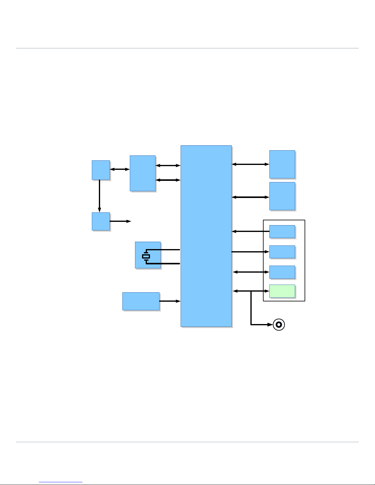
4.1 Board Block Diagram
The GR716-MINI Board provides the electrical functions and interfaces as represented in
the block diagram, Figure .4-2.
Note that not all features and interfaces are available at the same time, and the
configuration of on-board resistors plus programming of registers is required to access
some of the features.
GR716-MINI-UM, May 2019, Version 0.2 9 www.cobham.com/gaisler
Figure 4-1: GR716-MINI Board Block Diagram
CRYSTAL
CRYSTAL
SRAM
8 bit
SRAM
8 bit
GR716
MICRO-
CONTROLLER
GR716
MICRO-
CONTROLLER
13 x GPIO
13 x GPIO
JTAG
(FTDI-USB)
JTAG
(FTDI-USB)
EXPANSION CONNECTOR
DCDC
DCDC
MICRO
USB
MICRO
USB
SPI
FLASH
SPI
FLASH
LVDS in
(3 pairs)
LVDS in
(3 pairs)
LVDS out
(3 pairs)
LVDS out
(3 pairs)
12 x GPIO
12 x GPIO
4 x ANALOG
(ADC/DAC)
BOOTSTRAP/
CONFIGURATION
BOOTSTRAP/
CONFIGURATION
3.3V
DSU
2x UART
5V
Page 10

GR716-MINI
4.2 Board Mechanical Configuration
The board (50 x 35mm) and can be used 'stand-alone' on the bench-top simply using an
external USB cable as the main communication and power interface (+5V).
For mounting of the board on a carrier or expansion board, four M2 mounting holes are
provided in the corners of the board, as shown in the figure below.
GR716-MINI-UM, May 2019, Version 0.2 10 www.cobham.com/gaisler
Figure .4-2: GR716-MINI Board Dimensions (top side)
Figure .4-3: GR716-MINI Board Dimensions (bottom side - expansion connector)
Page 11

GR716-MINI
GR716-MINI-UM, May 2019, Version 0.2 11 www.cobham.com/gaisler
Figure 4-4: Example of a Carrier board
Page 12

GR716-MINI
4.3 GR716 Microcontroller
The Cobham Gaisler GR716 Microcontroller features a fault-tolerant LEON3 SPARC
V8 processor, communication interfaces and on-chip ADC, DAC, Power-on-Reset,
Oscillator, Brown-out detection, LVDS transceivers, regulators to support for single
3.3V supply, ideally suited for space and other high-rel applications.
The GR716 Microcontroller is a complex device with many modes of operation. For the
details of the interfaces, operation and programming, refer to[RD1].
The GR716 microcontroller is packaged in a 132-pin, 0.635mm pitch Ceramic Quad
Flat Pack package (housing: 24 x 24 mm).
GR716-MINI-UM, May 2019, Version 0.2 12 www.cobham.com/gaisler
Figure 4-5: GR716 Microcontroller Block Diagram
Figure 4-6: GR716 Package
Page 13

GR716-MINI
4.4 Memory
The memory configuration installed on the board comprises:
• 256 Mbit SPI serial boot prom (MX25L25635FZ2I-10G))
• 8 Mbit SRAM, 8 bit wide (CY7C1069G30)
The SPI boot memory is connected directly to the SPIM interface of the GR716 Microcontroller. Although the SPI memory can operate in a x4 data mode, on this board, only
a x1 data mode is used.
The SRAM is connected to the GR716 Microcontroller using the GPIO[50..49],
GPIO[34..0], GPIO[18..0] signals as shown in the figure below.
GR716-MINI-UM, May 2019, Version 0.2 13 www.cobham.com/gaisler
Figure 4-8: SRAM Signal Connections
Figure 4-7: SPI Boot Memory Connections
Page 14

GR716-MINI
4.5 Expansion/Interface Connector
To allow connection to external circuits, the bottom side of the board includes an 80 pin
low-profile expansion connector.
The connector pin out and type are listed in section 6.1 and the signals include:
EXT_CLK External 3.3V CMOS oscillator input for the main system clock, as
alternative to the on-board generated 20MHz clock
EXT_SPWCLK External 3.3V CMOS oscillator input for the Spacewire clock, as
alternative to the on-board generated 20MHz clock
3 x LVDS_IN pairs 3 LVDS input pairs, configurable acc section 4.6
3 x LVDS_OUT pairs 3 LVDS input pairs, configurable acc section 4.6
RESET_IN External input to reset circuit in GR716
RESET_OUT Output from reset circuit in GR716 for external use
VREF_BUF Buffered reference voltage output (1.000V nom.)
25 x GPIO (up to) 25 General purpose I/O signals, acc section 4.9
3.3V input Power input for external supply, acc section 4.13
Table 1: List of Expansion Connector signals
GR716-MINI-UM, May 2019, Version 0.2 14 www.cobham.com/gaisler
Figure 4-9: Expansion/Interface Connector
Page 15

GR716-MINI
4.6 LVDS Interfaces
The GR716 microcontroller provides a set of three LVDS input pairs and 3 LVDS
output pairs which are configurable from software via configuration registers to provide
SpaceWire or SPI4SPACE interfaces.
These signals are connected from the GR716 microcontroller to the Expansion
connector.
100 Ohm Termination resistors and fail-safe resistors for the LVDS receiver signals are
mounted on the board close to the receiver.
4.7 FTDI Serial to USB Interface
The GR716-MINI board provides an FTDI FT4232HL Serial to USB interface chip
which provides up to 4 serial ports which connect to a single Micro-B USB connector
(J1). This USB port can be connected to a host computer to allow communication over
serial interfaces to Host PC's which do not have conventional 9 pin D-sub type RS232
connectors.
On this board, the port assignment is as follows:
Pin Function Alternative signal
A-port DSU serial interface (DSURX, DSUTX) -
B-port Not assigned -
C-port UART port 2 (RXD,TXD,CTSN,RTSN) GPIO[59..56]
D-Port UART port 3 (RXD,TXD,CTSN,RTSN) GPIO[61..63]
Table 2: FTDI USB-Serial Port Assignment
GR716-MINI-UM, May 2019, Version 0.2 15 www.cobham.com/gaisler
Figure 4-10: Block diagram of FTDI Serial to USB Interface
GR716
HOST
TERMINAL/COMPUTER
USB
FTDI
DSU-SERIAL
UART2
UART3
Page 16

GR716-MINI
4.8 Analog Signals
The GR716-MINI board provides four micro-miniature (MMCX) coaxial connectors to
allow access to up to 4 ADC inputs or 4 DAC outputs of the GR716 microcontroller.
As shown in Figure 4-11, depending on which resistors are installed, each MMCX
connector can be either an ADC input or a DAC output.
Access to the ADC/DAC configurable from software via configuration registers, and for
further information please refer to [RD1]
The nominal input range for the ADC inputs is 0 – 2.0V
The DAC outputs are current outputs with a full-scale range of 0 – 4mA.
No current limiting or overvoltage protection components are
included on the GPIO/Analog signals of the GR716-MINI board.
The signals are connected directly from the microcontroller to the
coaxial/expansion connector. Care must therefore be taken to
ensure that any external circuitry connected does not exceed the
allowable voltage limits for the input/output pins.
GR716-MINI-UM, May 2019, Version 0.2 16 www.cobham.com/gaisler
Figure 4-11: MMCX analog connector interface
Page 17

GR716-MINI
4.9 GPIO
A total of 25 GPIO pins are connected from the GR716 Microcontroller to the
Expansion connector. These General purpose I/O pins are 3.3V LVCMOS voltage
levels. The following GPIO pins are connected.
Pin
Alternative function
GPIO55
-
GPIO54
-
GPIO53
-
GPIO52
-
GPIO51
-
GPIO48
DAC3
GPIO47
DAC2
GPIO46
DAC1
GPIO45
DAC0
GPIO44
ADC7
GPIO43
ADC6
GPIO42
ADC5
GPIO41
ADC4
GPIO40
ADC3
GPIO39
ADC2
GPIO38
ADC1
GPIO37
ADC0
GPIO36
-
GPIO35
-
GPIO24
-
GPIO23
-
GPIO22
-
GPIO21
-
GPIO20
-
GPIO19
-
Table 3: List of GPIO pins connected to Expansion Connector
Note: that some pins have a dual function and can be used instead
as ADC or DAC signals. Care must be taken to account for this.
No current limiting or overvoltage protection components are
included on the GPIO signals of the GR716-MINI board. The
signals are connected directly from the microcontroller to the
expansion connector. Care must therefore be taken to ensure that
any external circuitry connected does not exceed the allowable
voltage limits for the input/output pins.
GR716-MINI-UM, May 2019, Version 0.2 17 www.cobham.com/gaisler
Page 18

GR716-MINI
4.10 Bootstrap Signals
A number of features of the GR716 microcontroller are required to be set at power-on of
the processor, by means of bootstrap pins. A number of GPIO and function pins are predefined for this purpose.
Either the pull-up or the pull-down resistor should be installed to defined the desired
setting, according the definition Table 22 of [RD1].
Pin Function Pull-up
'1'
Pull-down
'0'
Default
GPIO0 Disable EDAC R4 R8 Pull-up
GPIO17 Bypass Internal Boot Prom R3 R7 Pull-down
GPIO62 Enable Memory Test R2 R6 Pull-down
GPIO63 Redundant Memory Available R1 R5 Pull-down
DSUTX Copy ASW image/SPW default frequency R23 R27 Pull-up
SPIM_MOSI Remote Access/Boot from Memory R32 R35 Pull-down
SPIM_SCK Boot Source 0 R31 R34 Pull-down
SPIM-SEL Boot Source 1 R30 R33 Pull-down
Table 4: Bootstrap Resistor Settings
GR716-MINI-UM, May 2019, Version 0.2 18 www.cobham.com/gaisler
Page 19

GR716-MINI
4.11 Debug Support Unit Interfaces
Program download and debugging to the processor is performed using the GRMON
Debug Monitor tool from Cobham Gaisler ([RD4]). The GR716 microcontroller
provides a UART based DSU interface for Debug and control of the processor by means
of a host terminal, as represented in Figure 4-12.
Four control signals from the Debug Support Unit interface to the processor are
implemented:
DSUTX Debug UART Transmit
DSURX Debug UART Receive
DSUEN This signal is pulled high on the board to enable Debugging
DSUBRE This signal is pulled low on the board
The DSUTX and DSURX signals are connected to the FTDI UART to USB converter
chip, allowing easy connection to a host PC using a USB cable.
GR716-MINI-UM, May 2019, Version 0.2 19 www.cobham.com/gaisler
Figure 4-12: Debug Support Unit connections
GR716
DSUBRE→
HOST
TERMINAL/COMPUTER
USB
DSUEN→
FTDI
DSURX→
DSUTX←
Page 20

GR716-MINI
4.12 Oscillators and Clock Inputs
The oscillator and clock scheme for the GR716-MINI Board is shown in Figure 4-13.
Two oscillator inputs are required: CLK for the main system clock, and SPW_CLK for
the SpaceWire clock of the microcontroller
To allow the GR716 Microcontroller to operate in a stand alone manner a soldered
20MHz crystal is installed on the board which connected to the Crystal oscillator
interface for the GR716.
This generates a 20MHz output clock, XO_OUT, which is connected to the CLK and
SPW_CLK inputs with zero-ohm resistors.
In an alternative scenario, it may be preferred to have a separate CLK or SYS_CLK to
allow different frequencies to be used. In this case the 0R resistors can be removed, and
instead the 'not-fitted' resistors be placed with zero-ohms to allow an external 3.3V
LVCMOS oscillator input to provided via the expansion connector.
For more details of the internal Crystal Oscillator, PLL structure and clock gating
features of the GR716, please refer to sections 9 and 10 of [RD1].
A separate 12 MHz crystal is required for the FTDI interface IC.
GR716-MINI-UM, May 2019, Version 0.2 20 www.cobham.com/gaisler
Figure 4-13: Board level Clock Distribution Scheme
GR716
microcontroller
GR716
microcontroller
SPW_CLK
CLK
XO_1
FTDI
PHY
FTDI
PHY
XTAL
12 MHz
Y2
XTAL
20 MHz
Y1
XO_2
XO_OUT
0R 0R
NF
NF
EXPANSION
CONNECTOR
EXPANSION
CONNECTOR
Page 21

GR716-MINI
4.13 Power Supply and Voltage Regulation
The power configuration is shown in Figure 4-14.
On this board, the microcontroller is configured to operate from a single +3.3V power
rail. The VDD_CORE (1.8V) is generated by a LDO regulator inside the GR716 itself.
To allow the board to be powered from the +5V supply provided on a standard USB
connector/cable, a LMZ21701 micro Point-of-Load regulator is included on the board
which generates the 3.3V for the rest of the GR716-MINI board.
In an alternative scenario, when the GR716-MINI board is installed on an Expansion
board or Motherboard, it is intended that the Motherboard should generate a regulated
3.3V supply and provide this via the Expansion connector.
In this configuration, the jumper JP1 should be removed to disconnect the USB cable
voltage, and the regulator is disabled by pulling its Enable signal low with the MB pin
on the expansion connector
Note: it is not the intention that the on-board POL regulator is used to provide
significant current toward other loads on the Expansion Board/Motherboard.
GR716-MINI-UM, May 2019, Version 0.2 21 www.cobham.com/gaisler
Figure 4-14: Power Regulation Scheme
VUSB
+3V3
DCDC
FT4232
GR716
5V nom.
17V max
LMZ21701
1A max
VDDA_ADC
3V3
VDDA_DAC
3V3
VDDA_REF
VDDA_LVDS
VDD_LDO_IN
VDD_IO
VDD_CORE
FILTER
FILTER
FILTER
SRAM
FLASH
EXPANSION
CONNECTOR
3V3
3V3
3V3
JP1
GND
MB
EN
USB cable
Page 22

GR716-MINI
4.14 Reset Circuit and Button
The GR716 microcontroller includes an internal RESET circuit with Brown-out detector
to reset the processor and its peripherals (see section 8 of [RD1]).
The resulting low reset signal is present on the microcontroller pin RESET_OUT_N.
This signal is connected to the expansion connector, P1.
To provide a manual reset of the microcontroller, a miniature push button switch, S1, is
provided on the PCB which connects to the RESET_IN_N signal.
This signal is also present on the expansion connector P1, and can be driven from an
external circuity if required.
4.15 Watchdog
The GR716 microcontroller includes an internal Watchdog timer function which can be
used for the purpose of generating a system reset in the event of a software malfunction
or crash. Please refer to [RD1].
GR716-MINI-UM, May 2019, Version 0.2 22 www.cobham.com/gaisler
Page 23

GR716-MINI
5 Setting Up and Using the Board
The board is provided with a default configuration set by bootstrap resistors. These
define the configuration at power on of the board
Other configurations may be defined by the user, by installing/removing the bootstrap
resistors.
For additional information, refer to [RD2] and for information about the Bootstrap
signals, refer to section 4.10.
There is one miniature jumper on the board as shown in Table 5.
Jumper Comment
JP1 Install to allow 5V supply from USB cable to provide power to the board.
Remove if board is installed on a motherboard and +3V3 power is provided
from the carrier board via connector P1
Table 5: Default Setting of Jumpers
To operate the board stand alone on the bench top, connect the board with a Micro USB
cable to a USB port on a host computer/laptop. This provides +5V supply to the board.
ATTENTION! To prevent damage to board, please ensure that the
correct power supply voltage and polarity is used with the board.
Do not exceed +17V at the power supply input, as this may damage
the board.
The POWER LED should be illuminated indicating that the power
supply is present and the board is generating the +3.3V it requires.
Upon power on, the Processor will start copy a ASW container from beginning at the
memory location 0x02000000, which is the start of the external SPI FLASH. If the SPI
FLASH is 'empty' or no valid program is installed, the first executed instruction will be
invalid, and the processor will halt with an ERROR condition.
To perform program download and software debugging on the hardware it is necessary
to use the Cobham Gaisler GRMON3 debugging software, installed on a host PC (as
represented in Figure 4-12). Please refer to the GRMON3 documentation for the
installation of the software on the host PC (Linux or Windows), and for the installation
of the associated hardware dongle.
To perform software download and debugging on the processor, a link from the Host
computer to the DSU interface of the board is necessary. As described in section 4.11
this is achieved via the FTDI USB interface.
Program download and debugging can be performed in the usual manner with
GRMON3. More information on the usage, commands and debugging features of
GRMON3, is given in the GRMON3 Users Manuals and associated documentation,
[RD4].
GR716-MINI-UM, May 2019, Version 0.2 23 www.cobham.com/gaisler
Page 24

GR716-MINI
6 Interfaces and Configuration
6.1 List of Connectors
Name Function Type Description
J1 FTDI-USB USB-Micro-B Configurable serial to USB I/F via FTDI chip
acc.ording section 4.7
J2 ANALOG-1 MMCX-jack Coaxial connector ADC-1 or DAC-1
J3 ANALOG-2 MMCX-jack Coaxial connector ADC-2 or DAC-2
J4 ANALOG-3 MMCX-jack Coaxial connector ADC-3 or DAC-3
J5 ANALOG-4 MMCX-jack Coaxial connector ADC-4 or DAC-4
PI EXPANSION HIROSE_FX11-80p Expansion connector
Table 6: List of Connectors
Pin Name Comment
1 VBUS +5V (from external host)
2 DM Data Minus
3 DP Data Plus
4 ID Not used
5 DGND Ground
Table 7: J1 USB type Micro B connector – FTDI Serial Link
Pin Name Comment
Inner ANALOG Refer to section 4.8
Outer AGND Ground
Table 8: J2,J3,J4,J5 MMCX miniature coax connectors
GR716-MINI-UM, May 2019, Version 0.2 24 www.cobham.com/gaisler
Page 25

GR716-MINI
Table 9: Expansion connector P1 Pin-out
GR716-MINI-UM, May 2019, Version 0.2 25 www.cobham.com/gaisler
Page 26

GR716-MINI
6.2 List of Oscillators, Switches and LED's
Name Function Description
Y1 USB-XTAL 20 MHz, SMD soldered
Y2 FTDI-XTAL 12 MHz, SMD soldered
Table 10: List and definition of Oscillators and Crystals
Name Function Description
D1 POWER 3.3V power
Table 11: List and definition of PCB mounted LED's
Name Function Description
S1 RESET Push button RESET switch
Table 12: List and definition of Switches
GR716-MINI-UM, May 2019, Version 0.2 26 www.cobham.com/gaisler
Page 27

GR716-MINI
GR716-MINI-UM, May 2019, Version 0.2 27 www.cobham.com/gaisler
Figure 6-1: PCB Top View
Figure 6-2: PCB Bottom View
Page 28

GR716-MINI
GR716-MINI-UM, May 2019, Version 0.2 28 www.cobham.com/gaisler
Figure 6-3: PCB Top View (Photo)
Figure 6-4: PCB Bottom View (Photo)
Page 29

GR716-MINI
7 Change Record
Issue Date Section / Page Description
0.0 2018-10-18 All Draft Issue
0.1 2018-11-25 4.10 Updated default bootstraps to match SPI Flash boot
5 Corrected start address
4.2 Swapped figure 4-3
0.2 2019-05-02
All Corrected frequency of crystal and default bootstrap
GR716-MINI-UM, May 2019, Version 0.2 29 www.cobham.com/gaisler
Page 30

GR716-MINI
Cobham Gaisler AB
Kungsgatan 12
411 19 Göteborg
Sweden
www.cobham.com/gaisler
sales@gaisler.com
T: +46 31 7758650
F: +46 31 421407
Cobham Gaisler AB, reserves the right to make changes to any products and services described herein at any
time without notice. Consult Cobham or an authorized sales representative to verify that the information in
this document is current before using this product. Cobham does not assume any responsibility or liability
arising out of the application or use of any product or service described herein, except as expressly agreed
to in writing by Cobham; nor does the purchase, lease, or use of a product or service from Cobham convey a
license under any patent rights, copyrights, trademark rights, or any other of the intellectual rights of
Cobham or of third parties. All information is provided as is. There is no warranty that it is correct or suitable
for any purpose, neither implicit nor explicit.
Copyright © 2019 Cobham Gaisler AB
GR716-MINI-UM, May 2019, Version 0.2 30 www.cobham.com/gaisler
 Loading...