

Page 1

GR716-CPCI-DEV
Development Board
2019 User's Manual
The most important thing we build is trust
GR716-CPCI-DEV
Development Board
User's Manual
GR716-CPCI-DEV-UM, 2019, Version 0.2 www.cobham.com/gaisler
Page 2

GR716-CPCI-DEV
Intentionally Blank
GR716-CPCI-DEV-UM, May 2019, Version 0.2 2 www.cobham.com/gaisler
Page 3

GR716-CPCI-DEV
Table of Contents
1 Introduction......................................................................................................................7
1.1 Scope of the Document.......................................................................................7
1.2 Reference Documents..........................................................................................7
2 Abbreviations...................................................................................................................8
3 Introduction......................................................................................................................9
3.1 Overview.............................................................................................................9
3.2 Handling............................................................................................................11
4 Board Design..................................................................................................................12
4.1 Board Block Diagram........................................................................................12
4.2 Board Mechanical Configuration......................................................................13
4.3 GR716-BOARD and Expansion Boards...........................................................14
4.4 Interface Configuration Board...........................................................................16
4.5 GPIO..................................................................................................................17
4.6 SPW...................................................................................................................17
4.7 SPI4S.................................................................................................................17
4.8 LVDS.................................................................................................................18
4.9 UART-A / UART-B / UART-C..........................................................................18
4.10 CAN...................................................................................................................18
4.11 MIL1553............................................................................................................19
4.12 SPI0 / SPI1........................................................................................................19
4.13 PACKETWIRE..................................................................................................19
4.14 DAC0-3 & ADC0-7...........................................................................................19
4.15 Bootstrap Signals...............................................................................................19
4.16 Debug Support Unit Interfaces..........................................................................20
4.17 Oscillators and Clock Inputs.............................................................................21
4.18 Power Supply and Voltage Regulation..............................................................21
4.19 Reset Circuit and Button...................................................................................22
5 Setting Up and Using the Board...................................................................................23
6 Interfaces and Configuration.......................................................................................24
6.1 List of Connectors.............................................................................................24
6.2 List of Headers..................................................................................................33
6.3 List of Oscillators, Switches and LED's............................................................33
GR716-CPCI-DEV-UM, May 2019, Version 0.2 3 www.cobham.com/gaisler
Page 4

GR716-CPCI-DEV
7 Change Record...............................................................................................................39
GR716-CPCI-DEV-UM, May 2019, Version 0.2 4 www.cobham.com/gaisler
Page 5

GR716-CPCI-DEV
List of Figures
Figure 3-1: GR716-CPCI-DEV Development Board...........................................................................9
Figure 4-1: GR716-CPCI-DEV Board Block Diagram......................................................................12
Figure 4-2: GR716-CPCI-DEV Board Dimensions...........................................................................13
Figure 4-3: GR716-BOARD mounted on a GR716-CPCI-DEV Carrier board.................................14
Figure 4-4: GR716-BOARD..............................................................................................................15
Figure 4-5: GR716-TEST-MEMORY BOARD.................................................................................15
Figure 4-6: Interface Configuration Board.........................................................................................16
Figure 4-7: Installed Interface Configuration Board..........................................................................16
Figure 4-8: GPIO interface.................................................................................................................17
Figure 4-9: Dual purpose LVDS Signal Header.................................................................................18
Figure 4-10: Debug Support Unit connections...................................................................................20
Figure 4-11: Power Regulation Scheme.............................................................................................22
Figure 6-1: GR716-CPCI-DEV Front Panel......................................................................................25
Figure 6-2: PCB Top View.................................................................................................................35
Figure 6-3: PCB Bottom View...........................................................................................................36
Figure 6-4: PCB Top View (Photo)....................................................................................................37
Figure 7-1: PCB Bottom View (Photo)..............................................................................................38
GR716-CPCI-DEV-UM, May 2019, Version 0.2 5 www.cobham.com/gaisler
Page 6

GR716-CPCI-DEV
List of Tables
Table 1: UART interface Combinations.............................................................................................18
Table 2: Bootstrap Resistor Settings...................................................................................................20
Table 3: List of Connectors................................................................................................................24
Table 4: Expansion connector P1 & P2 Pin-out.................................................................................26
Table 5: Expansion connector P3 & P4 Pin-out.................................................................................26
Table 6: J1 USB type Micro B connector – FTDI Serial Link...........................................................27
Table 7: J2 GPIO Header Pin out.......................................................................................................27
Table 8: J3 GPIO Header Pin out.......................................................................................................28
Table 9: J4 GPIO Header Pin out.......................................................................................................28
Table 10: J5 GPIO Header Pin out.....................................................................................................29
Table 11: J6 SPW/SPI4S Header........................................................................................................29
Table 12: J7 SPW-0 Header................................................................................................................30
Table 13: J8 SPI4S-R Connector........................................................................................................30
Table 14: J9, J10, J11 UART Interface Headers.................................................................................30
Table 15: J12 CAN Interface Headers................................................................................................30
Table 16: J13 CAN Interface Headers................................................................................................31
Table 17: J14 & J15 CAN Interface Headers.....................................................................................31
Table 18: J15 PW Interface Headers..................................................................................................31
Table 19: J17-J31 MMCX miniature coax connectors.......................................................................31
Table 20: J32 POWER – External Power Connector.........................................................................31
Table 21: J33 POWER – External Power Connector - Alternative....................................................32
Table 22: J34 Power-Out connector...................................................................................................32
Table 23: J35, J36, J36 Connectors for Interface Configuration........................................................32
Table 24: List of Jumpers...................................................................................................................33
Table 25: List and definition of Oscillators and Crystals...................................................................33
Table 26: List and definition of PCB mounted LED's........................................................................33
Table 27: List and definition of Switches...........................................................................................33
Table 28: Definition of Switch S1 functions......................................................................................34
GR716-CPCI-DEV-UM, May 2019, Version 0.2 6 www.cobham.com/gaisler
Page 7

GR716-CPCI-DEV
1 Introduction
1.1 Scope of the Document
This document provides a User's Manual and Interface document for the “GR716CPCI-DEV” Development and Demonstration board.
The work has been performed by Cobham Gaisler AB, Göteborg, Sweden.
1.2 Reference Documents
[RD1] GR716, Data Sheet and User's Manual",Cobham Gaisler, GR716-UM-DS, available
from http://www.gaisler.com/index.php/products/components/GR716
[RD2] GR716-CPCI-DEV_schematic.pdf, Schematic
[RD3] GR716-CPCI-DEV_assy_drawing.pdf, Assembly Drawing
[RD4] GRMON3 User's Manual, available from:
https://www.gaisler.com/index.php/products/debug-tools/grmon3
[RD5] GR716-BOARD User Manual.pdf, User Manual
GR716-CPCI-DEV-UM, May 2019, Version 0.2 7 www.cobham.com/gaisler
Page 8

GR716-CPCI-DEV
2 Abbreviations
ASIC Application Specific Integrated Circuit.
DSU Debug Support Unit
EDAC Error Detection and Correction
ESA European Space Agency
ESD Electro-Static Discharge
ESTEC European Space Research and Technology Center
GPIO General Purpose Input / Output
IC Integrated Circuit
I/O Input/Output
IP Intellectual Property
LDO Low Drop-Out
PCB Printed Circuit Board
POL Point of Load
SOC System On a Chip
SPW Spacewire
TBC To Be Confirmed
TBD To Be Defined
GR716-CPCI-DEV-UM, May 2019, Version 0.2 8 www.cobham.com/gaisler
Page 9
GR716-CPCI-DEV
3 Introduction
3.1 Overview
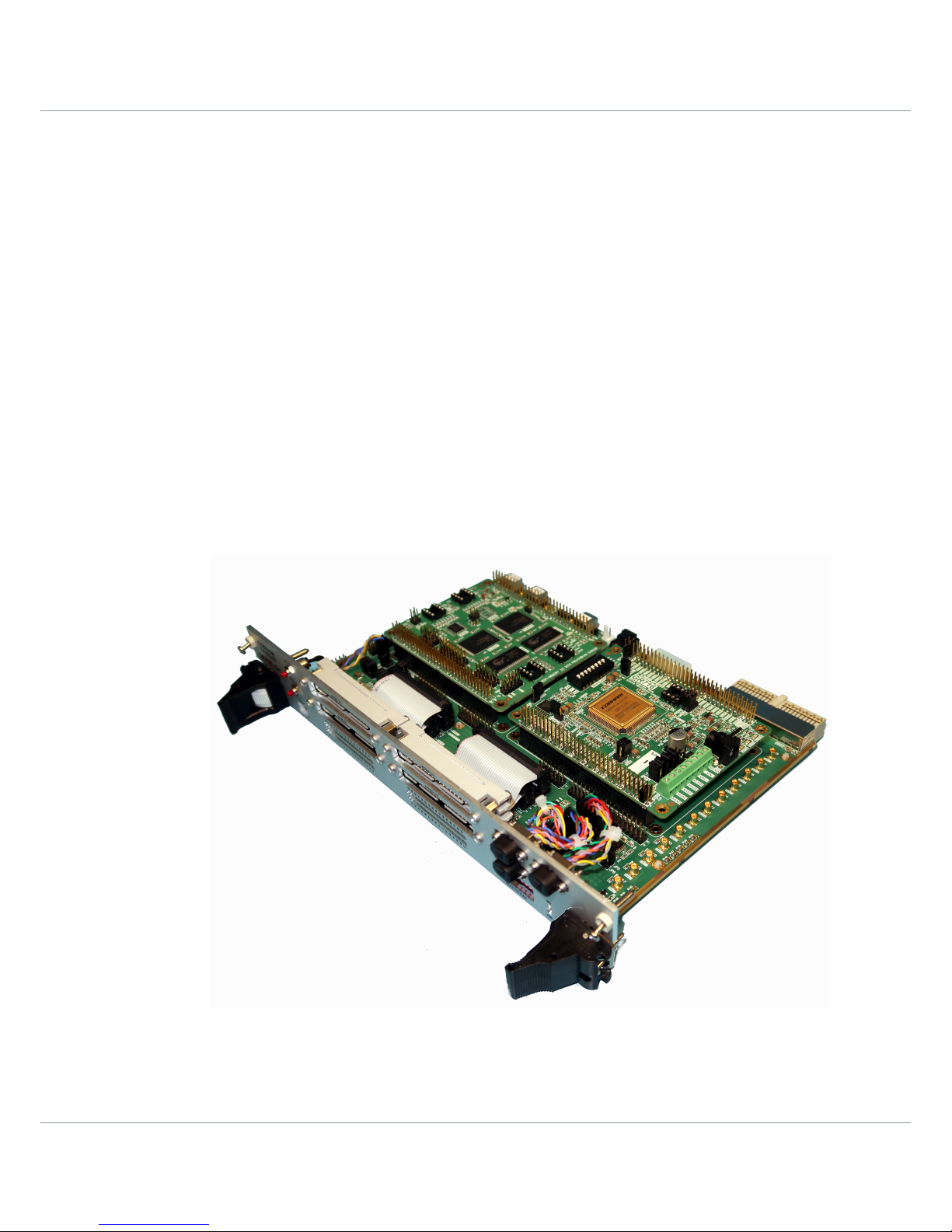
This document describes the GR716-CPCI-DEV Development Board.
Together with the GR716-DEV board, this equipment is intended to be used as a
platform for the demonstration of the Cobham Gaisler GR716 RAD Hard
Microcontroller.
Furthermore, this board provides developers with a convenient hardware platform for
the evaluation and development of software for the GR716 microcontroller, and allows
the GR716-DEV board to be installed in a CPCI rack for further integration with other
development equipment.
The GR716 Microcontroller features a fault-tolerant LEON3 SPARC V8 processor,
communication interfaces and on-chip ADC, DAC, Power-on-Reset, Oscillator, Brownout detection, LVDS transceivers, regulators to support for single 3.3V supply, ideally
suited for space and other high-rel applications.
GR716-CPCI-DEV-UM, May 2019, Version 0.2 9 www.cobham.com/gaisler
Figure 3-1: GR716-CPCI-DEV Development Board
Page 10

GR716-CPCI-DEV
The board contains the following main items as detailed in section 4 of this document:
• CPCI 6U format (233.35 x 160mm)
• two sites for plug on modules with two 2x32 pin stackable 0.1” headers
• plug on board for configuration of interface routing to peripherals
• connector for single VIN power input (+5V to +12V)
• front panel with
◦ 0.1” header connectors for 64 GPIO signals (plus ground)
◦ LED’s as status indicators for GPIO signals
◦ two Spacewire connecotrs (MDM9S)
◦ connector for SPI4Space interface (MDM9S)
◦ DIP switch for bootstrap settings
◦ mini USB connector for FTDI-USB interface
◦ LED indicators for Power and ResetOut status
◦ RESET_IN and DSUBREAK push button switches
• on-board headers for ribbon cable connection to
◦ Packetwire interface
◦ CAN interface
◦ DSU plus UART interfaces
◦ MIL1553 interface
◦ SPI peripherals
• miniature coax connectors for 8 x ADC and 4 x DAC analog signals
• jumpers for power supply configuration
• on-board regulators converting from VIN to 3.3V & 1.8V
• sockets for optional on-board oscillator s for
◦ SYSCLK
◦ SPWCLK
◦ MIL1553CLK
◦ PWMCLK
GR716-CPCI-DEV-UM, May 2019, Version 0.2 10 www.cobham.com/gaisler
Page 11

GR716-CPCI-DEV
3.2 Handling
ATTENTION: OBSERVE PRECAUTIONS FOR
HANDLING ELECTROSTATIC SENSITIVE DEVICES
This unit contains sensitive electronic components which can be damaged by
Electrostatic Discharges (ESD). When handling or installing the unit observe
appropriate precautions and ESD safe practices.
When not in use, store the unit in an electrostatic protective container or bag.
When configuring the jumpers on the board, or connecting/disconnecting cables, ensure
that the unit is in an un-powered state.
When operating the board in a 'stand-alone' configuration, the power supply should be
current limited to prevent damage to the board or power supply in the event of an overcurrent situation.
This board is intended for commercial use and evaluation in a standard laboratory
environment, nominally, 20°C. All devices are standard commercial types, intended for
use over the standard commercial operating temperature range (0 to 70ºC).
GR716-CPCI-DEV-UM, May 2019, Version 0.2 11 www.cobham.com/gaisler
Page 12
GR716-CPCI-DEV
4 Board Design
4.1 Board Block Diagram
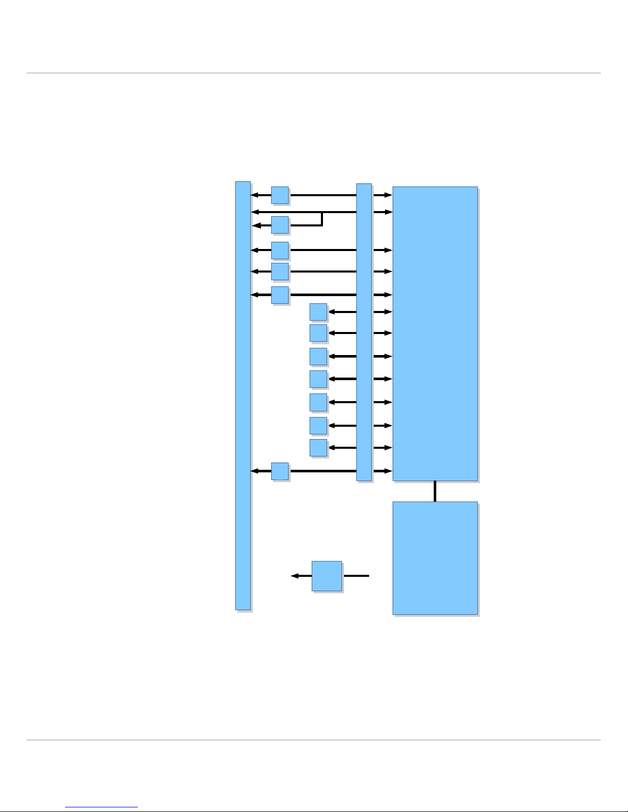
The GR716-CPCI-DEV Board provides the electrical functions and interfaces as
represented in the block diagram Figure 4-1.
Note that not all features and interfaces are simultaneously available since the pins of
the GR716 microcontroller have multiple functions. The available interfaces depends on
the configuration and programming of the registers of the GR716 Microcontroller, and
on the connections made by the Interface Configuration Module.
GR716-CPCI-DEV-UM, May 2019, Version 0.2 12 www.cobham.com/gaisler
Figure 4-1: GR716-CPCI-DEV Board Block Diagram
EXPANSION
SLOT FOR
GR716-BOARD
EXPANSION
SLOT FOR
GR716-BOARD
DCDC
DCDC
3.3V
VIN
FRONT PANEL
FRONT PANEL
EXPANSION
SLOT FOR
GR716-TEST-
MEMORY
OR USER
EXPANSION
EXPANSION
SLOT FOR
GR716-TEST-
MEMORY
OR USER
EXPANSION
GPIO (64x)
FTDI USB
GPIO-LED
(64x)
SPW
SPI4S
SPW/SPI4S
CAN
7 x UART
PW
MIL1553
2 x SPI
4 x DAC
8 x ADC
BOOTSTRAP
INTERFACE CONFIGURATION MODULE
INTERFACE CONFIGURATION MODULE
Page 13

GR716-CPCI-DEV
4.2 Board Mechanical Configuration
The board (233.35 x 160mm) and can be used 'stand-alone' on the bench-top simply an
external +12V power supply connected to connector J32.
A 6U format, 2 slot sized CPCI front panel is fitted to allow the board to be installed in
a CPCI rack.
GR716-CPCI-DEV-UM, May 2019, Version 0.2 13 www.cobham.com/gaisler
Figure 4-2: GR716-CPCI-DEV Board Dimensions
Page 14

GR716-CPCI-DEV
4.3 GR716-BOARD and Expansion Boards
The GR716-CPCI-DEV provides two sites with two 2x32 pin headers to allow the board
to function as a carrier board for the GR716-BOARD (Figure 4-4).
The first set of headers (P1, P2) is intended for mounting the GR716-BOARD as shown
in Figure 4-3
The second set of headers connect with a one-to-one correspondence with the first set
and is intended for the mounting a GR716-TEST-MEMORY board (Figure 4-5), to
provide the GR716-BOARD with extended FLASH and SRAM external memory.
Alternatively, the second set of headers provides a convenient way for User Defined
interface boards to be developed and connected to the GR716-CPCI-DEV, if other
functions or features are to be demonstrated.
GR716-CPCI-DEV-UM, May 2019, Version 0.2 14 www.cobham.com/gaisler
Figure 4-3: GR716-BOARD mounted on a GR716-CPCI-DEV Carrier board
Page 15

GR716-CPCI-DEV
GR716-CPCI-DEV-UM, May 2019, Version 0.2 15 www.cobham.com/gaisler
Figure 4-4: GR716-BOARD
Figure 4-5: GR716-TEST-MEMORY BOARD
Page 16

GR716-CPCI-DEV
4.4 Interface Configuration Board
Since the GR716 microcontroller has pins with multiple functions, it is necessary to
have a way to route pins from the GR716-BOARD to the interface circuits in a way that
prevents signal and interface conflicts.
This is achieved on the GR716-CPCI-DEV board by means of Interface configuration
Boards as shown in Figure 4-6.
These boards can be configured by means of installing or removing solder bridges in
order to route connections from the GPIO pins of the GR716-BOARD to the interface
circuits on the GR716-CPCI-BOARD.
The organisation of the solder bridges corresponds with the organisation of the IO
Configuration Options shown in Table 7 of [RD1].
The Interface Configuration Board mounts on to the GR716-CPCI-DEV board
undernearth the Expansion Board, as shown in Figure 4-7.
GR716-CPCI-DEV-UM, May 2019, Version 0.2 16 www.cobham.com/gaisler
Figure 4-7: Installed Interface Configuration Board
Figure 4-6: Interface Configuration Board
Page 17

GR716-CPCI-DEV
4.5 GPIO
All 64 GPIO pins can be connected from the GR716-BOARD via the Expansion
Connector to the GR716-CPCI-DEV.
These 64 general Purpose Input Output signals (3.3V LVCMOS voltage levels) are
connected to a set of 0.1” pitch pin headers and from there via ribbon cable the front
panel of the GR716-CPCI-DEV board, thus allowing easy access to these signals, either
individually, or with a ribbon cable connection. A series protection resistor of 470 Ohm
is included on each signal at the front panel connector.
To indicate the state of the GPIO pins, LED indicators are provided on the front panel.
Note that the state of some of the GPIO pins are sampled at power-up or reset of the
processor in order to determine initial conditions of a number of internal features, as
listed in Table 22 of [RD1] and as described in section 4.15.
4.6 SPW
The GR-CPCI-DEV board provides LVDS transceivers to connect the dedicated
SpaceWire interface signals of the GR716 microcontroller to a 10 pin header J7. This
header is connected with wire tails to a MDM9S connector on the front panel to provide
a standard SpaceWire interface.
4.7 SPI4S
The GR-CPCI-DEV board provides LVDS transceivers to connect the dedicated
SPI4SPACE interface signals of the GR716 microcontroller to a 10 pin header J8. This
header is connected with wire tails to a MDM9S connector on the front panel.
GR716-CPCI-DEV-UM, May 2019, Version 0.2 17 www.cobham.com/gaisler
Figure 4-8: GPIO interface
IO
CONFIGURAT ION
BOARD
PCB
64
GPIO[63..0]
SERIES
RESISTOR
470R
(x64)
GPIO[63..0]
GR716BOARD
Page 18

GR716-CPCI-DEV
4.8 LVDS
The dedicated LVDS interface signals from the GR716 microcontroller are connected to
a 10 pin header J6. Depending on the configuration of the GR716 microcontroller and
Interface Configuration board,, this interface can be used as SpaceWire or as a
SPI4SPACE interface.
This header is connected with wire tails to a MDM9S connector on the front panel.
4.9 UART-A / UART-B / UART-C
Three 20 pin headers are provided on the GR716-CPCI-DEV board to allow various
combinations of UART interfaces to be connected with a ribbon cable to a GR-CPCI-
6U-UART accessory board. This can provide up to 6 UART interfaces with RS232
transceivers and standard DSUB-9S connectors
The Headers provide the following combinations of interfaces:
Header
J9
Header
J10
Header J11 Comment
UART0 UART2 UART4 RX, TX, CTSN, RTSN signals
UART1 UART3 UART5 RX, TX, CTSN, RTSN signals
UART2 UART4 UART0 RX & TX signal
UART3 UART5 UART1 RX & TX signal
UART4 UART0 UART2 RX & TX signal
- UART1 UART3 RX & TX signal
UART-DSU - - RX & TX signal
Table 1: UART interface Combinations
4.10 CAN
The CAN signals from the GR716-BOARD are connected to a header J12.
GR716-CPCI-DEV-UM, May 2019, Version 0.2 18 www.cobham.com/gaisler
Figure 4-9: Dual purpose LVDS Signal Header
Page 19

GR716-CPCI-DEV
To provide the necessary CAN transceiver circuits, this header can be connected with a
ribbon cable to a GR-PCI-CAN accessory board.
4.11 MIL1553
The MIL1553 signals from the GR716-BOARD are connected to a header J13.
To provide the necessary MIL-1553 transceiver circuits, this header can be connected
with a ribbon cable to a GR-ACC-GR740 accessory board.
4.12 SPI0 / SPI1
The signals of the SPI0 and SPI1 interfaces from the GR716-BOARD are connected to a
header J14 & J15 respectively.
This header can be connected with a custom cable to a GR-ACC-GR740 accessory
board.
4.13 PACKETWIRE
The signals of the SPI0 and SPI1 interfaces from the GR716-BOARD are connected to a
header J16.
This header can be connected with a custom cable to a GR-TMTC-PW accessory board.
Note though that the GR-TMTC-PW does not accommodate the TX_READY and
RX_READY signals.
4.14 DAC0-3 & ADC0-7
The four DAC current outputs from the GR716-BOARD are connected to a miniature
MMCX coaxial connectors J17 to J20.
The eight ADC voltage inputs to the GR716-BOARD are connected to a miniature
MMCX coaxial connectors J21 to J27 and J29.
4.15 Bootstrap Signals
A number of features of the GR716 microcontroller are required to be set at power-on of
the processor, by means of bootstrap pins. A number of GPIO and function pins are predefined for this purpose, according the definition Table 22 of [RD1].
To define the desired setting, an 8 pole, DIP switch (S1), is provided on the front panel
of the GR716-CPCI-DEV board to connect these signals to DGND or via pull-up to
3V3.
Note: A DIP switch for setting these Bootstrap signals also exists on the GR716-
BOARD ([RD5]). The DIP switches on the GR716-BOARD should be set to ‘float’ to
ensure that there is no conflict with the DIP switch settings on the front panel of the
GR716-CPCI-DEV board.
GR716-CPCI-DEV-UM, May 2019, Version 0.2 19 www.cobham.com/gaisler
Page 20

GR716-CPCI-DEV
Pin Function Open Closed Default
GPIO0 Disable EDAC ‘1’ ‘0’ ‘1’
GPIO17 Bypass Internal Boot Prom ‘1’ ‘0’ ‘0’
GPIO62 Enable Memory Test ‘1’ ‘0’ ‘0’
GPIO63 Redundant Memory Available ‘1’ ‘0’ ‘0’
DSUTX Copy ASW image/SPW default frequency ‘1’ ‘0’ ‘0’
SPIM_MOSI Remote Access/Boot from Memory ‘1’ ‘0’ ‘0’
SPIM_SCK Boot Source 0 ‘1’ ‘0’ ‘0’
SPIM-SEL Boot Source 1 ‘1’ ‘0’ ‘0’
Table 2: Bootstrap Resistor Settings
4.16 Debug Support Unit Interfaces
Program download and debugging to the processor is performed using the GRMON
Debug Monitor tool from Cobham Gaisler ([RD4]). The GR716 microcontroller
provides a UART based DSU interface for Debug and control of the processor by means
of a host terminal, as represented in Figure 4-10.
Four control signals from the Debug Support Unit interface to the processor are
implemented:
DSUTX Debug UART Transmit
DSURX Debug UART Receive
DSUEN This signal is pulled high on the board to enable Debugging
DSUBRE This signal is pulled low on the board
These signals are connected via the Expansion Connector interface from the GR716-
BOARD to an FTDI USB interface. This allows a USB connection to be made to a host
computer.
GR716-CPCI-DEV-UM, May 2019, Version 0.2 20 www.cobham.com/gaisler
Figure 4-10: Debug Support Unit connections
GR716-BOARD
DSUBRE→
HOST
TERMINAL/COMPUTER
USB
DSUEN
→
FTDI
DSUR
X
→
DSUTX
←
EXPANSION
CONNECTOR
Page 21

GR716-CPCI-DEV
4.17 Oscillators and Clock Inputs
The GR716-CPCI-DEV Board provides four DIL sockets to allow an external oscillator
clocks to be connected to the following clock inputs of the GR716 microcontroller:
EXT_SYSCLK
EXT_SPWCLK
EXT_1553_CLK
EXT_PWMCLK
For more details of the internal Crystal Oscillator, PLL structure and clock gating
features of the GR716, please refer to sections 9 and 10 of [RD1].
4.18 Power Supply and Voltage Regulation
The power configuration is represented in Figure 4-11.
The main voltage supply input can be provided from one of the following sources:
1. VIN input supply via connector J33.
2. VIN input supply via connector J34.
3. VIN provided via CPCI Backplane connector
VIN is regulated on the GR716-CPCI-DEV board to with a local Point-of-Load DC/DC
converter to generate a +3V3 voltage supply for the local circuits on the GR716-CPCI-
DEV board.
VIN is also connected to the GR716-BOARD via the expansion connector P2, where it
is further regulated for the GR716 microcontroller, as described in [RD5].
The VIN voltage should have a nominal value of 12V. However, due to the wide input
voltage range capability of the POL DC/DC converters used, the input voltage may
range from 5V to 17V.
Note though that, due to the 15V transzorb protection diode on the GR716-CPCI-DEV
board, the input voltage on this board should not exceed 14.5V.
GR716-CPCI-DEV-UM, May 2019, Version 0.2 21 www.cobham.com/gaisler
Page 22

GR716-CPCI-DEV
4.19 Reset Circuit and Button
The GR716 microcontroller includes an internal RESET circuit with Brown-out detector
to reset the processor and its peripherals (see section 8 of [RD1]).
The resulting low reset signal is present on the microcontroller pin RESET_OUT_N.
This signal is connected to the expansion connector, P2.
A manual reset of the microcontroller can be generated using the RESET_IN_N signal.
This signal is present on the expansion connector P2, and can be driven from an
external circuity if required. A miniature push button switch is provided on the front
panel of the GR716-CPCI-DEV board to pull this signal low, when the button is pressed.
GR716-CPCI-DEV-UM, May 2019, Version 0.2 22 www.cobham.com/gaisler
Figure 4-11: Power Regulation Scheme
J33
+3V3
DCDC
5V min
12V nom
14.5V max
LMZ21701
+3V3
CPCI
CONNECTOR
J32
+VIN
EXPANSION
CONNECTOR
P2
EXPANSION
CONNECTOR
P4
Page 23

GR716-CPCI-DEV
5 Setting Up and Using the Board
The board is provided with a default configuration set by bootstrap settings.
For additional information, refer to [RD2] and for information about the Bootstrap
signals, refer to section 4.15.
To operate the board stand alone on the bench top, install the power configuration
jumpers appropriately, and +12V supply to the board connector J32.
ATTENTION! To prevent damage to board, please ensure that the
correct power supply voltage and polarity is used with the board.
Do not exceed +14.5V at the power supply input, as this may
damage the board.
The POWER_3V3 power good LED on the front panel should be
illuminated indicating that the power supply is present and the
board is generating the supply voltages that it requires.
Upon power on, the Processor will start executing instructions beginning at the memory
location 0x02000000, which is the start of the external SPI Flash. If the SPI Flash is
'empty' or no valid program is installed, the first executed instruction will be invalid,
and the processor will halt with an ERROR condition.
To perform program download and software debugging on the hardware it is necessary
to use the Cobham Gaisler GRMON3 debugging software, installed on a host PC (as
represented in Figure 4-10). Please refer to the GRMON3 documentation for the
installation of the software on the host PC (Linux or Windows), and for the installation
of the associated hardware dongle.
To perform software download and debugging on the processor, a link from the Host
computer to the DSU interface of the board is necessary. As described in section 4.16
this is achieved via the FTDI USB interface.
Program download and debugging can be performed in the usual manner with
GRMON3. More information on the usage, commands and debugging features of
GRMON3, is given in the GRMON3 Users Manuals and associated documentation,
[RD4].
GR716-CPCI-DEV-UM, May 2019, Version 0.2 23 www.cobham.com/gaisler
Page 24

GR716-CPCI-DEV
6 Interfaces and Configuration
6.1 List of Connectors
Name Function Type Description
PI EXPANSION-1 2x32 pin 0.1” Header Expansion connector-1
P2 EXPANSION-2 2x32 pin 0.1” Header Expansion connector-2
P3 EXPANSION-1 2x32 pin 0.1” Header Expansion connector-3
P4 EXPANSION-2 2x32 pin 0.1” Header Expansion connector-4
J1 FTDI-USB Mini USB FTDI Serial to USB interface
J2 GPIO[15..0] 2x17 pin 0.1” Header GPIO signals 0-15
J3 GPIO[31..16] 2x17 pin 0.1” Header GPIO signals 16-31
J4 GPIO[47..32] 2x17 pin 0.1” Header GPIO signals 32-47
J5 GPIO[63..48] 2x17 pin 0.1” Header GPIO signals 48-63
J6 SPW0 2x5 pin 0.1” Header Connects to front panel MDM9S connector
J7 SPW1 2x5 pin 0.1” Header Connects to front panel MDM9S connector
J8 SPI4S 2x5 pin 0.1” Header Connects to front panel MDM9S connector
J9 UART-A 2x10 pin 0.1” Header
J10 UART-B 2x10 pin 0.1” Header
J11 UART-C 2x10 pin 0.1” Header
J12 CAN 2x10 pin 0.1” Header
J13 MIL1553 2x10 pin 0.1” Header
J14 SPI0 2x6 pin 0.1” Header
J15 SPI1 2x6 pin 0.1” Header
J16 PACKETWIRE 2x10 pin 0.1” Header Interface signals for Packetwire interface
J17-J20 DAC0-3 MMCX
J21-J27 ADC0-6 MMCX
J28 EXT_SYSCLK MMCX
J29 ADC0-7 MMCX
J30 EXT_SPWCLK MMCX
J31 EXT_PWMCLK MMCX
J32 POWER-IN 2.1mm, centre +ve VIN (nominal +12V)
J33 POWER-IN 4 pin MOLEX Alternative power in connector (nom. +12V)
J34 POWER-OUT 2 pin MOLEX6410 Header for TBD use
J35-J37 IO-CONFIG HIROSE FX11-100S Connectors for IO ‘personality’ module
CPCI-J1 CPCI CPCI interface connector – power only
Table 3: List of Connectors
GR716-CPCI-DEV-UM, May 2019, Version 0.2 24 www.cobham.com/gaisler
Page 25

GR716-CPCI-DEV
GR716-CPCI-DEV-UM, May 2019, Version 0.2 25 www.cobham.com/gaisler
Figure 6-1: GR716-CPCI-DEV Front Panel
Page 26

GR716-CPCI-DEV
Table 4: Expansion connector P1 & P2 Pin-out
Table 5: Expansion connector P3 & P4 Pin-out
GR716-CPCI-DEV-UM, May 2019, Version 0.2 26 www.cobham.com/gaisler
Page 27

GR716-CPCI-DEV
Pin Name Comment
1 VBUS +5V (from external host)
2 DM Data Minus
3 DP Data Plus
4 ID Not used
5 DGND Ground
Table 6: J1 USB type Micro B connector – FTDI Serial Link
Function Connector Pin Function
GPIO0
1
■ □
2
DGND
GPIO1
3
□ □
4
DGND
GPIO2
5
□ □
6
DGND
GPIO3
7
□ □
8
DGND
GPIO4
9
□ □
10
DGND
GPIO5
11
□ □
12
DGND
GPIO6
13
□ □
14
DGND
GPIO7
15
□ □
16
DGND
GPIO8
17
□ □
18
DGND
GPIO9
19
□ □
20
DGND
GPIO10
21
□ □
22
DGND
GPIO11
23
□ □
24
DGND
GPIO12
25
□ □
26
DGND
GPIO13
27
□ □
28
DGND
GPIO14
29
□ □
30
DGND
GPIO15
31
□ □
32
DGND
(+3.3V)
33
□ □
34
DGND
Table 7: J2 GPIO Header Pin out
GR716-CPCI-DEV-UM, May 2019, Version 0.2 27 www.cobham.com/gaisler
Page 28

GR716-CPCI-DEV
Function Connector Pin Function
GPIO16
1
■ □
2
DGND
GPIO17
3
□ □
4
DGND
GPIO18
5
□ □
6
DGND
GPIO19
7
□ □
8
DGND
GPIO20
9
□ □
10
DGND
GPIO21
11
□ □
12
DGND
GPIO22
13
□ □
14
DGND
GPIO23
15
□ □
16
DGND
GPIO24
17
□ □
18
DGND
GPIO25
19
□ □
20
DGND
GPIO26
21
□ □
22
DGND
GPIO27
23
□ □
24
DGND
GPIO28
25
□ □
26
DGND
GPIO29
27
□ □
28
DGND
GPIO30
29
□ □
30
DGND
GPIO31
31
□ □
32
DGND
(+3.3V)
33
□ □
34
DGND
Table 8: J3 GPIO Header Pin out
Function Connector Pin Function
GPIO32
1
■ □
2
DGND
GPIO33
3
□ □
4
DGND
GPIO34
5
□ □
6
DGND
GPIO35
7
□ □
8
DGND
GPIO36
9
□ □
10
DGND
GPIO37
11
□ □
12
DGND
GPIO38
13
□ □
14
DGND
GPIO39
15
□ □
16
DGND
GPIO40
17
□ □
18
DGND
GPIO41
19
□ □
20
DGND
GPIO42
21
□ □
22
DGND
GPIO43
23
□ □
24
DGND
GPIO44
25
□ □
26
DGND
GPIO45
27
□ □
28
DGND
GPIO46
29
□ □
30
DGND
GPIO47
31
□ □
32
DGND
(+3.3V)
33
□ □
34
DGND
Table 9: J4 GPIO Header Pin out
GR716-CPCI-DEV-UM, May 2019, Version 0.2 28 www.cobham.com/gaisler
Page 29

GR716-CPCI-DEV
Function Connector Pin Function
GPIO48
1
■ □
2
DGND
GPIO49
3
□ □
4
DGND
GPIO50
5
□ □
6
DGND
GPIO51
7
□ □
8
DGND
GPIO52
9
□ □
10
DGND
GPIO53
11
□ □
12
DGND
GPIO54
13
□ □
14
DGND
GPIO55
15
□ □
16
DGND
GPIO56
17
□ □
18
DGND
GPIO57
19
□ □
20
DGND
GPIO58
21
□ □
22
DGND
GPIO59
23
□ □
24
DGND
GPIO60
25
□ □
26
DGND
GPIO61
27
□ □
28
DGND
GPIO62
29
□ □
30
DGND
GPIO63
31
□ □
32
DGND
(+3.3V)
33
□ □
34
DGND
Table 10: J5 GPIO Header Pin out
Table 11: J6 SPW/SPI4S Header
(Pins 1-9 connect 1:1 to MDM9S on front panel)
GR716-CPCI-DEV-UM, May 2019, Version 0.2 29 www.cobham.com/gaisler
Page 30

GR716-CPCI-DEV
Table 12: J7 SPW-0 Header
(Pins 1-9 connect 1:1 to MDM9S on front panel)
Table 13: J8 SPI4S-R Connector
(Pins 1-9 connect 1:1 to MDM9S on front panel)
Table 14: J9, J10, J11 UART Interface Headers
Table 15: J12 CAN Interface Headers
GR716-CPCI-DEV-UM, May 2019, Version 0.2 30 www.cobham.com/gaisler
Page 31

GR716-CPCI-DEV
Table 16: J13 CAN Interface Headers
Table 17: J14 & J15 CAN Interface Headers
Table 18: J15 PW Interface Headers
Pin Name Comment
Inner SIGNAL Signal
Outer AGND Ground
Table 19: J17-J31 MMCX miniature coax connectors
Pin Name Comment
+VE +VIN Inner Pin, +5V to +12V, typically 1 A
-VE DGND Outer Pin Return
Table 20: J32 POWER – External Power Connector
GR716-CPCI-DEV-UM, May 2019, Version 0.2 31 www.cobham.com/gaisler
Page 32

GR716-CPCI-DEV
Pin Name Comment
1 +VIN +VIN (+12V nominal)
2 DGND Ground
3 DGND Ground
4 nc Not connected
Table 21: J33 POWER – External Power Connector - Alternative
Pin Name Comment
1 DGND Ground
2 +VIN +VIN (+12V nominal)
Table 22: J34 Power-Out connector
Table 23: J35, J36, J36 Connectors for Interface Configuration
GR716-CPCI-DEV-UM, May 2019, Version 0.2 32 www.cobham.com/gaisler
Page 33

GR716-CPCI-DEV
6.2 List of Headers
Name Function Type Description
JP1 RESET/BREAK 2x2 pin 0.1” Header Conn. to front panel push button switches
JP2 I2C 2x3 pin 0.1” Header Enable I2C connection to FTDI interface
JP3 UART-0 2x4 pin 0.1” Header Enable UART-0 connection to FTDI interface
JP4 UART-1 2x4 pin 0.1” Header Enable UART-1 connection to FTDI interface
JP5 SPI4S 1x2 pin 0.1” Header Disable SPI4S interface
Table 24: List of Jumpers
6.3 List of Oscillators, Switches and LED's
Name Function Description
X1 EXT_PWMCLCK 8 pin DIL socket for TBD MHz 3.3V oscillator
X2 EXT_SYSCLK 8 pin DIL socket for TBD MHz 3.3V oscillator
X3 EXT_SPWCLCK 8 pin DIL socket for TBD MHz 3.3V oscillator
X4 EXT_MIL1553 8 pin DIL socket for TBD MHz 3.3V oscillator
Y1 FTDI clock 12 MHz crystal, SMD soldered
Table 25: List and definition of Oscillators and Crystals
Name Function Description
D1A/B-D32A/B GPIO 64 LED indicators for GPIO signal status
D33A POWER_3V3 3.3V power good
D33B RESET_OUT RESET_OUT signal from GR716-BOARD
Table 26: List and definition of PCB mounted LED's
Name Function Description
S1 8 pole SPDT DIP switch Pull-up/Float/Pull-Down Bootstrap settings – see Table 28
Table 27: List and definition of Switches
GR716-CPCI-DEV-UM, May 2019, Version 0.2 33 www.cobham.com/gaisler
Page 34

GR716-CPCI-DEV
Name Function Description
S1-1 GPIO0 Disable EDAC
S1-2 GPIO17 Bypass Internal Boot PROM
S1-3 GPIO62 Enable Memory Test
S1-4 GPIO63 Redundant Memory available
S1-5 DSUTX Copy ASW image
S1-6 SPIM_SEL Boot Source 0
S1-7 SPIM-SCK Boot Source 1
S1-8 SPIM-MOSI Remote access/Boot from memory
Table 28: Definition of Switch S1 functions
(refer to [RD1])
GR716-CPCI-DEV-UM, May 2019, Version 0.2 34 www.cobham.com/gaisler
Page 35

GR716-CPCI-DEV
GR716-CPCI-DEV-UM, May 2019, Version 0.2 35 www.cobham.com/gaisler
Figure 6-2: PCB Top View
Page 36

GR716-CPCI-DEV
GR716-CPCI-DEV-UM, May 2019, Version 0.2 36 www.cobham.com/gaisler
Figure 6-3: PCB Bottom View
Page 37

GR716-CPCI-DEV
GR716-CPCI-DEV-UM, May 2019, Version 0.2 37 www.cobham.com/gaisler
Figure 6-4: PCB Top View (Photo)
Page 38

GR716-CPCI-DEV
GR716-CPCI-DEV-UM, May 2019, Version 0.2 38 www.cobham.com/gaisler
Figure 7-1: PCB Bottom View (Photo)
Page 39

GR716-CPCI-DEV
7 Change Record
Issue Date Section / Page Description
0.0 2019-05-02 All Draft Issue
0.1 2019-11-25 4.15 Updated default values
5 Updated boot start address
6.3 Updated function for GPIO[0] and GPIO[17]
0.2 2019-05-02 All Corrected typos
GR716-CPCI-DEV-UM, May 2019, Version 0.2 39 www.cobham.com/gaisler
Page 40

GR716-CPCI-DEV
Cobham Gaisler AB
Kungsgatan 12
411 19 Göteborg
Sweden
www.cobham.com/gaisler
sales@gaisler.com
T: +46 31 7758650
F: +46 31 421407
Cobham Gaisler AB, reserves the right to make changes to any products and services described herein at any
time without notice. Consult Cobham or an authorized sales representative to verify that the information in
this document is current before using this product. Cobham does not assume any responsibility or liability
arising out of the application or use of any product or service described herein, except as expressly agreed
to in writing by Cobham; nor does the purchase, lease, or use of a product or service from Cobham convey a
license under any patent rights, copyrights, trademark rights, or any other of the intellectual rights of
Cobham or of third parties. All information is provided as is. There is no warranty that it is correct or suitable
for any purpose, neither implicit nor explicit.
Copyright © 2019 Cobham Gaisler AB
GR716-CPCI-DEV-UM, May 2019, Version 0.2 40 www.cobham.com/gaisler
 Loading...