

Page 1
GR716
LEON3FT Microcontroller
2019 Advanced Data Sheet and User’s Manual
The most important thing we build is trust
Features
• Fault-tolerant SPARC V8 processor with 31 register
windows, 192KiB EDAC protected tightly coupled
memory and support for reduced instruction set.
• Double precision IEEE-754 floating point unit
• Advanced on-chip debug support unit
• Memory protection units
• 8-bit external PROM/SRAM interface with BCH EDAC
protection
• Boot from external SRAM/PROM, SPI or I
2
C memory
protected by EDAC and dual memory redundancy
• SpaceWire interface with time distribution support
• SPI for Space master and slave interface
• MIL-STD-1553B interface
• CAN 2.0B controller interface
• PacketWire with CRC acceleration support
• On-chip 12-bit DAC and two 11-bit ADC
• Programmable PWM interface
• UARTs, SPI, I
2
C, GPIO, Timers with Watchdog, Inter-
rupt controller, Status registers, UART debug, etc.
• Configurable I/O switch matrix
Floating
Point
Unit
Local
Dual-port
Instruction
RAM
Main bus
FTMCTRL
UART
I2CMST /
I2CSLV
SPICTRL
GRGPIO
GRPULSE
GRPWM
On-chip
LDO
Integer
Unit
AMBA
Interface
On-chip
Oscillator
PLL
Debug
Support
Unit
Local
Dual-port
Data
RAM
Memory
Scrubber
SPIMCTRL
IRQ Control
Timers
AHBSTAT
GRADCDAC
On-chip DAC
On-chip ADC
Brownout
Detector
Power-on
reset
LEON3
Statistics
Unit
Debug bus
DMA bus
AHB2AHB
Bridge
AHBROM
MEMPROT
CLKGATE
GPREG
LSTAT
UART
Dbg Link
AHB2AHB
Bridge
AHB
Trace
DMA
Controller
APBCTRL
Bridges
1553B
SpaceWire
I2C to AHB
SPI to AHB
GRPWRX
(MAP)
GRPWTX
GRCAN
AHB
UART
Description
The GR716 device is a fault-tolerant LEON3
SPARC V8 processor with various communication
interfaces and on-chip ADC, DAC, Power-onReset, Oscillator, Brown-out detection, LVDS
transceivers, regulators to support single 3.3V
supply, ideally suited for space and other high-rel
applications.
Specification
• System frequency up-to 50 MHz
• SpaceWire links up-to 100 Mbps
• CQFP132 hermetically sealed ceramic package
• Total Ionizing Dose (TID) up to 100 krad (Si)
• Single-Event Latch-up Immunity (SEL) to LET
> 118 MeV-cm
• Single-Event Upset (SEU) below 10
2
mg
-6
errors per
TH
device and day in space environment (TBC)
• Support for single 3.3V supply
Applications
The GR716 microcontroller is an advanced microcontroller, targeting high reliability space and aeronautics applications.
Support for many different standard interfaces makes
the GR716 microcontroller ideal for supervision, monitoring and control in a satellite, such as:
• propulsion system control
• sensor bus control
• robotics applications control
• simple motor control
• mechanism control
• power control
• particle detector instrumentation
• radiation environment monitoring
• thermal control
• antenna pointing control
• AOCS / GNC (Gyro, IMU, MTM)
• remote terminal unit control
• simple instrument control
• wireless networking
Availability
The GR716 microcontroller is currently available as engineering samples. Contact Cobham Gaisler for information on flight model schedule.
GR716-DS-UM, May 2019, Version 1.29 www.cobham.com/gaisler
Page 2

GR716
1 Introduction.............................................................................................................................. 9
1.1 Scope .......................................................................................................................................................9
1.2 Data sheet limitations ..............................................................................................................................9
1.3 Updates and feedback.............................................................................................................................. 9
1.4 Software support...................................................................................................................................... 9
1.5 Reference documents ..............................................................................................................................9
1.6 Document revision history .................................................................................................................... 10
1.7 Acronyms ..............................................................................................................................................13
1.8 Definitions .............................................................................................................................................14
1.9 Register descriptions .............................................................................................................................15
2 Architecture............................................................................................................................ 16
2.1 Key features...........................................................................................................................................17
2.2 Digital Architecture Overview .............................................................................................................. 20
2.3 Analog Architecture Overview.............................................................................................................. 28
2.4 Signal Overview....................................................................................................................................32
2.5 I/O switch matrix overview................................................................................................................... 32
2.6 I/O switch default configurations for bootstraps...................................................................................35
2.7 I/O switch matrix options, considerations and limitations .................................................................... 38
2.8 I/O switch matrix pin validation script.................................................................................................. 39
2.9 I/O switch matrix scenario examples ....................................................................................................42
2.10 Cores......................................................................................................................................................48
2.11 Memory map .........................................................................................................................................49
2.12 Interrupts ...............................................................................................................................................54
3 Signals.................................................................................................................................... 56
3.1 Bootstrap signals ...................................................................................................................................56
3.2 Configuration for flight ......................................................................................................................... 63
3.3 Complete signal list ............................................................................................................................... 64
4 Clocking................................................................................................................................. 66
4.1 PLL Configuration and Status...............................................................................................................67
4.2 Clock Source and divisor ......................................................................................................................67
4.3 System clock.......................................................................................................................................... 68
4.4 SpaceWire clock.................................................................................................................................... 68
4.5 MIL-STD-1553B clock .........................................................................................................................68
4.6 PacketWire RX Clock ........................................................................................................................... 68
4.7 ADC Clock ............................................................................................................................................68
4.8 DAC Clock ............................................................................................................................................69
4.9 PWM Clock...........................................................................................................................................69
4.10 Clock gating unit ...................................................................................................................................69
4.11 Debug AHB bus clocking......................................................................................................................69
4.12 Test mode clocking................................................................................................................................ 69
5 Reset....................................................................................................................................... 70
5.1 IO Reset.................................................................................................................................................70
6 Technical notes....................................................................................................................... 71
6.1 GRLIB AMBA plug&play scanning.....................................................................................................71
6.2 Software portability...............................................................................................................................71
7 System Startup Status and General Configuration................................................................. 72
7.1 Configuration Registers......................................................................................................................... 72
7.2 Boot Strap information register.............................................................................................................77
GR716-DS-UM, May 2019, Version 1.29 2 www.cobham.com/gaisler
Page 3

GR716
7.3 Special Configuration Registers ............................................................................................................78
8 Reset Generation and Brownout Detection............................................................................ 86
8.1 Overview ...............................................................................................................................................86
8.2 Operation ...............................................................................................................................................86
8.3 Registers ................................................................................................................................................ 87
9 Crystal (XO) Oscillator.......................................................................................................... 91
9.1 Overview ...............................................................................................................................................91
9.2 Operation ...............................................................................................................................................91
10 PLL......................................................................................................................................... 93
10.1 Overview ...............................................................................................................................................93
10.2 Operation ...............................................................................................................................................93
10.3 Registers ................................................................................................................................................ 94
11 Voltage and Current References........................................................................................... 100
11.1 Overview .............................................................................................................................................100
11.2 Operation .............................................................................................................................................100
12 ADC, Pre-Amplifier and Analog MUX ............................................................................... 101
12.1 Overview .............................................................................................................................................101
12.2 Operation .............................................................................................................................................102
12.3 Registers .............................................................................................................................................. 107
13 LDO ..................................................................................................................................... 112
13.1 Overview ............................................................................................................................................. 112
13.2 Operation ............................................................................................................................................. 112
14 Temperature Sensor.............................................................................................................. 113
14.1 Overview ............................................................................................................................................. 113
14.2 Operation ............................................................................................................................................. 113
15 DAC ..................................................................................................................................... 114
15.1 Overview ............................................................................................................................................. 114
15.2 Operation ............................................................................................................................................. 115
15.3 Registers .............................................................................................................................................. 116
16 LEON3/FT - High-performance SPARC V8 32-bit Processor ............................................ 119
16.1 Overview ............................................................................................................................................. 119
16.2 LEON3 integer unit .............................................................................................................................120
16.3 Local instruction and data RAM .........................................................................................................128
16.4 Floating-point unit...............................................................................................................................128
16.5 AMBA interface .................................................................................................................................. 129
16.6 Configuration registers ........................................................................................................................130
16.7 Software considerations ......................................................................................................................136
17 IEEE-754 Floating-Point Unit ............................................................................................. 137
17.1 Overview .............................................................................................................................................137
17.2 Functional Description ........................................................................................................................137
18 UART Serial Interface ......................................................................................................... 140
18.1 Overview .............................................................................................................................................141
18.2 Operation .............................................................................................................................................141
18.3 Baud-rate generation ........................................................................................................................... 142
18.4 Loop back mode .................................................................................................................................. 143
18.5 FIFO debug mode................................................................................................................................143
GR716-DS-UM, May 2019, Version 1.29 3 www.cobham.com/gaisler
Page 4

GR716
18.6 Interrupt generation .............................................................................................................................143
18.7 Registers .............................................................................................................................................. 144
19 Hardware Debug Support Unit ............................................................................................ 147
19.1 Overview .............................................................................................................................................147
19.2 Operation .............................................................................................................................................147
19.3 AHB trace buffer .................................................................................................................................148
19.4 Instruction trace buffer ........................................................................................................................150
19.5 Using the DSU trace buffer .................................................................................................................151
19.6 DSU memory map...............................................................................................................................151
19.7 DSU registers ...................................................................................................................................... 152
20 On-chip Dual-port Memory with EDAC Protection............................................................ 158
20.1 Overview .............................................................................................................................................158
20.2 Local Memory memory map and register ...........................................................................................161
21 Fault Tolerant PROM/SRAM Memory Interface ................................................................ 165
21.1 Overview .............................................................................................................................................165
21.2 PROM access ......................................................................................................................................166
21.3 SRAM access ......................................................................................................................................168
21.4 Memory EDAC ................................................................................................................................... 168
21.5 Bus Ready signalling...........................................................................................................................169
21.6 Access errors .......................................................................................................................................171
21.7 Registers .............................................................................................................................................. 172
22 Fault Tolerant NVRAM Memory Interface ......................................................................... 176
23 MIL-STD-1553B / AS15531 Interface ................................................................................ 177
23.1 Overview .............................................................................................................................................177
23.2 Electrical interface............................................................................................................................... 178
23.3 Operation .............................................................................................................................................178
23.4 Bus Controller Operation .................................................................................................................... 180
23.5 Remote Terminal Operation ................................................................................................................185
23.6 Bus Monitor Operation........................................................................................................................189
23.7 Registers .............................................................................................................................................. 190
24 ADC / DAC Interface .......................................................................................................... 202
24.1 Overview .............................................................................................................................................202
24.2 Operation .............................................................................................................................................204
24.3 Registers .............................................................................................................................................. 206
25 CAN 2.0 Controller.............................................................................................................. 211
25.1 Overview ............................................................................................................................................. 211
25.2 Interface............................................................................................................................................... 213
25.3 Protocol ...............................................................................................................................................213
25.4 Status and monitoring.......................................................................................................................... 214
25.5 Transmission........................................................................................................................................ 214
25.6 Reception.............................................................................................................................................217
25.7 Global reset and enable ....................................................................................................................... 220
25.8 Registers .............................................................................................................................................. 221
25.9 Memory mapping ................................................................................................................................ 230
26 Clock gating unit (Primary) ................................................................................................. 232
26.1 Overview .............................................................................................................................................232
26.2 Operation .............................................................................................................................................232
GR716-DS-UM, May 2019, Version 1.29 4 www.cobham.com/gaisler
Page 5

GR716
26.3 Registers .............................................................................................................................................. 233
27 Clock gating unit (Secondary) ............................................................................................. 236
27.1 Overview .............................................................................................................................................236
27.2 Operation .............................................................................................................................................236
27.3 Registers .............................................................................................................................................. 237
28 DMA Controller with internal AHB/APB bridge ................................................................240
28.1 Overview .............................................................................................................................................240
28.2 Configuration.......................................................................................................................................241
28.3 Operation .............................................................................................................................................250
28.4 AHB transfers......................................................................................................................................252
28.5 Interrupts .............................................................................................................................................252
28.6 Errors ...................................................................................................................................................252
28.7 Internal Buffer Readout Interface........................................................................................................ 253
28.8 Registers .............................................................................................................................................. 253
28.9 DMA Transfer Example ...................................................................................................................... 259
29 General Purpose I/O Port ..................................................................................................... 263
29.1 Overview .............................................................................................................................................264
29.2 Operation .............................................................................................................................................264
29.3 Pulse command....................................................................................................................................264
29.4 Pulse sequencer ...................................................................................................................................264
29.5 Pulse sampler......................................................................................................................................266
29.6 Registers .............................................................................................................................................. 266
30 Pulse Width Modulation Generator ..................................................................................... 277
30.1 Overview .............................................................................................................................................278
30.2 Operation .............................................................................................................................................278
30.3 Registers .............................................................................................................................................. 280
31 PacketWire Receiver............................................................................................................ 285
31.1 Overview .............................................................................................................................................285
31.2 PacketWire interface............................................................................................................................ 285
31.3 Operation .............................................................................................................................................286
31.4 Operation .............................................................................................................................................286
31.5 Registers .............................................................................................................................................. 288
32 PacketWire Transmitter........................................................................................................ 291
32.1 Overview .............................................................................................................................................291
32.2 PacketWire interface............................................................................................................................ 291
32.3 Operation .............................................................................................................................................292
32.4 Registers .............................................................................................................................................. 293
33 SpaceWire Interface and RMAP target................................................................................ 296
33.1 Overview .............................................................................................................................................296
33.2 Operation .............................................................................................................................................297
33.3 Link interface ...................................................................................................................................... 298
33.4 Time-code distribution ........................................................................................................................ 301
33.5 Interrupt distribution............................................................................................................................302
33.6 Receiver DMA channels......................................................................................................................304
33.7 Transmitter DMA channels ................................................................................................................. 310
33.8 RMAP..................................................................................................................................................313
33.9 AMBA interface .................................................................................................................................. 317
GR716-DS-UM, May 2019, Version 1.29 5 www.cobham.com/gaisler
Page 6

GR716
33.10 SpaceWire Plug-and-Play....................................................................................................................318
33.11 Registers .............................................................................................................................................. 324
34 SpaceWire - Time Distribution Protocol.............................................................................. 342
34.1 Overview .............................................................................................................................................342
34.2 Protocol ...............................................................................................................................................342
34.3 Functionality........................................................................................................................................342
34.4 Data formats ........................................................................................................................................348
34.5 Reference documents ..........................................................................................................................348
34.6 Registers .............................................................................................................................................. 349
35 General Purpose Timer Unit with Watchdog ....................................................................... 365
35.1 Overview .............................................................................................................................................365
35.2 Operation .............................................................................................................................................365
35.3 Registers .............................................................................................................................................. 367
36 General Purpose Timer Unit (Secondary)............................................................................ 371
36.1 Overview .............................................................................................................................................371
36.2 Operation .............................................................................................................................................371
36.3 Registers .............................................................................................................................................. 372
37 I2C to AHB bridge............................................................................................................... 376
37.1 Overview .............................................................................................................................................376
37.2 Operation .............................................................................................................................................377
37.3 Registers .............................................................................................................................................. 381
38 I2C master ............................................................................................................................ 384
38.1 Overview .............................................................................................................................................384
38.2 Operation .............................................................................................................................................385
38.3 Registers .............................................................................................................................................. 388
39 I2C slave .............................................................................................................................. 391
39.1 Overview .............................................................................................................................................391
39.2 Operation .............................................................................................................................................392
39.3 Registers .............................................................................................................................................. 394
40 Interrupt Controller .............................................................................................................. 398
40.1 Overview .............................................................................................................................................398
40.2 Operation .............................................................................................................................................399
40.3 Registers .............................................................................................................................................. 403
41 LEON3 Statistics Unit ......................................................................................................... 415
41.1 Overview .............................................................................................................................................415
41.2 Using the LEON3 statistics unit.......................................................................................................... 417
41.3 Registers .............................................................................................................................................. 417
42 Memory Scrubber and Status Register ................................................................................ 420
42.1 Overview .............................................................................................................................................421
42.2 Operation .............................................................................................................................................421
42.3 Registers .............................................................................................................................................. 423
43 SPI to AHB bridge ............................................................................................................... 428
43.1 Overview .............................................................................................................................................428
43.2 Transmission protocol .........................................................................................................................429
43.3 System clock requirements and sampling ...........................................................................................430
43.4 SPI instructions....................................................................................................................................430
GR716-DS-UM, May 2019, Version 1.29 6 www.cobham.com/gaisler
Page 7

GR716
43.5 Registers .............................................................................................................................................. 432
44 SPI Controller ...................................................................................................................... 434
44.1 Overview .............................................................................................................................................434
44.2 Operation .............................................................................................................................................435
44.3 Registers .............................................................................................................................................. 438
45 SPI for Space Slave Controller ............................................................................................ 445
45.1 Overview .............................................................................................................................................445
45.2 Implementation of SPI protocols......................................................................................................... 446
45.3 Transmission........................................................................................................................................ 446
45.4 Operation .............................................................................................................................................447
45.5 SPI 2 Protocol Handler........................................................................................................................447
45.6 Message Header - Command Token.................................................................................................... 448
45.7 Redundancy ......................................................................................................................................... 454
45.8 Registers .............................................................................................................................................. 455
46 SPI Memory Controller........................................................................................................ 460
46.1 Overview .............................................................................................................................................461
46.2 Operation .............................................................................................................................................461
46.3 Registers .............................................................................................................................................. 464
47 AMBA Protection Unit ........................................................................................................ 467
47.1 Overview .............................................................................................................................................467
47.2 Operation .............................................................................................................................................468
47.3 Registers .............................................................................................................................................. 468
47.4 Example of configure and use the Memory protection .......................................................................484
48 Serial Debug and remote access Interface ........................................................................... 486
48.1 Overview .............................................................................................................................................487
48.2 Operation .............................................................................................................................................487
48.3 Registers .............................................................................................................................................. 488
49 AHB Status Registers .......................................................................................................... 490
49.1 Overview .............................................................................................................................................490
49.2 Operation .............................................................................................................................................490
49.3 Registers .............................................................................................................................................. 491
50 Trace buffer.......................................................................................................................... 493
50.1 Overview .............................................................................................................................................493
50.2 Operation .............................................................................................................................................494
50.3 Using the AHB trace buffer................................................................................................................. 495
50.4 Registers .............................................................................................................................................. 496
51 Boot ROM............................................................................................................................ 499
51.1 Overview .............................................................................................................................................499
51.2 ROM Architecture............................................................................................................................... 500
51.3 Loader description............................................................................................................................... 505
51.4 Standby description ............................................................................................................................. 505
51.5 State at handover to application software............................................................................................506
51.6 Boot source requirements.................................................................................................................... 507
51.7 Protection schemes.............................................................................................................................. 507
52 Electrical description ........................................................................................................... 510
52.1 Absolute maximum ratings .................................................................................................................510
52.2 Recommended operating conditions ................................................................................................... 512
GR716-DS-UM, May 2019, Version 1.29 7 www.cobham.com/gaisler
Page 8

GR716
52.3 Power supplies characteristics............................................................................................................. 513
52.4 Input voltages, leakage currents and capacitances .............................................................................. 514
52.5 Output voltages, leakage currents and capacitances ........................................................................... 515
52.6 Simplified IO buffer schematics..........................................................................................................517
52.7 DAC Electrical Characteristics ........................................................................................................... 519
52.8 ADC Electrical Characteristics ........................................................................................................... 520
52.9 Reference Voltages and Currents Electrical Characteristics ............................................................... 524
52.10 Reset and Brownout-Detector Electrical Characteristics ....................................................................524
52.11 AC characteristics................................................................................................................................526
53 Mechanical description ........................................................................................................540
53.1 Component and package .....................................................................................................................540
53.2 Pin assignment.....................................................................................................................................540
53.3 Mechanical package drawings............................................................................................................. 544
54 Ordering information ........................................................................................................... 546
55 Errata .................................................................................................................................... 547
55.1 Overview .............................................................................................................................................547
55.2 Errata description ................................................................................................................................ 547
56 Features ................................................................................................................................ 549
56.1 Overview .............................................................................................................................................549
56.2 Feature description .............................................................................................................................. 549
GR716-DS-UM, May 2019, Version 1.29 8 www.cobham.com/gaisler
Page 9

GR716
1 Introduction
1.1 Scope
This document is the advanced data sheet and user’s manual for the GR716 LEON3FT microcontroller. The GR716 microcontroller has been developed in an activity initiated by the European Space
Agency under ESTEC contract 40001117749/14/NL/AK.
1.2 Data sheet limitations
Note that this document is an advanced data sheet:
• Advanced data sheet - Product in development
• Preliminary data sheet - Shipping prototype
• Data sheet - Shipping space-grade product
1.3 Updates and feedback
Feedback can be sent to:
Cobham Gaisler AB support: support@gaisler.com
1.4 Software support
The GR716 LEON3FT microcontroller design is supported by standard toolchains provided by
Cobham Gaisler. Toolchains can be downloaded from http://www.cobham.com/gaisler.
1.5 Reference documents
[AMBA] AMBA Specification, Rev 2.0, ARM Limited
[GRLIB] GRLIB IP Library User's Manual, Cobham Gaisler, www.cobham.com/gaisler
[GRIP] GRLIB IP Core User's Manual, Cobham Gaisler, www.cobham.com/gaisler
[SPARC] The SPARC Architecture Manual, Version 8, SPARC International Inc.
[LEON-REX] LEON-REX Instruction Set Extension, Cobham Gaisler
[GRMON3] GRMON3 User's Manual, Cobham Gaisler
GR716-DS-UM, May 2019, Version 1.29 9 www.cobham.com/gaisler
Page 10

GR716
1.6 Document revision history
Change record information is provided in table 1.
Table 1. Change record
Version Date Note
1.29 May 2019 First public release
GR716-DS-UM, May 2019, Version 1.29 10 www.cobham.com/gaisler
Page 11

GR716
1.7 Acronyms
Table 2. Acronyms
Acronym Comment
AHB Advanced High-performance bus, part of [AMBA]
AMBA Advanced Microcontroller Bus Architecture
APB Advanced Peripheral Bus, part of [AMBA]
BCH Bose–Chaudhuri–Hocquenghem, class of error-correcting codes
CAN Controller Area Network, bus standard
CPU Central Processing Unit, used to refer to one LEON4 processor core.
DMA Direct Memory Access
DSU Debug Support Unit
EDAC Error Detection and Correction
FIFO First-In-First-Out, refers to buffer type
FPU Floating Point Unit
Gb
GB
GiB
Gigabit, 10
Gigabyte, 10
Gibibyte, gigabinary byte, 2
9
bits
9
bytes
30
bytes, unit defined in IEEE 1541-200
I/O Input/Output
ISR Interrupt Service Routine
JTAG Joint Test Action Group (developer of IEEE Standard 1149.1-1990)
kB
KiB
Mb, Mbit
MB, Mbyte
MiB
Kilobyte, 10
Kibibyte, 2
Megabit, 10
Megabyte, 10
Mebibyte, 2
3
bytes
10
bytes, unit defined in IEEE 1541-2002
6
bits
6
bytes
20
bytes, unit defined in IEEE 1541-2002
PROM Programmable Read Only Memory
RAM Random Access Memory
SEE Single Event Effects
SEL/SEU/
Single Event Latchup/Upset/Transient
SET
SPARC Scalable Processor ARChitecture
SW Software
UART Universal Asynchronous Receiver/Transmitter
GR716-DS-UM, May 2019, Version 1.29 11 www.cobham.com/gaisler
Page 12

GR716
1.8 Definitions
This section and the following subsections define the typographic and naming conventions used
throughout this document.
1.8.1 Bit numbering
The following conventions are used for bit numbering:
• The most significant bit (MSb) of a data type has the leftmost position
• The least significant bit of a data type has the rightmost position
• Unless otherwise indicated, the MSb of a data type has the highest bit number and the LSb the
1.8.2 Radix
The following conventions is used for writing numbers:
• Binary numbers are indicated by the prefix "0b", e.g. 0b1010.
• Hexadecimal numbers are indicated by the prefix "0x", e.g. 0xF00F
• Unless a radix is explicitly declared, the number should be considered a decimal.
lowest bit number
1.8.3 Data types
Byte (BYTE) 8 bits of data
Halfword (HWORD) 16 bits of data
Word (WORD) 32 bits of data
GR716-DS-UM, May 2019, Version 1.29 12 www.cobham.com/gaisler
Page 13
GR716
1.9 Register descriptions
An example register, showing the register layout used throughout this document, can be seen
in table 3. The values used for the reset value fields are described in table 4, and the values
used for the field type fields are described in table 5. Fields that are named RESERVED,
RES, or R are read-only fields. These fields can be written with zero or with the value read
from the same register field.
Table 3. <Address> - <Register acronym> - <Register name>
31 24 23 16 15 8 7 0
EF3 EF2 EF1 EF0
<Reset value for EF3> <Reset value for EF2> <Reset value for EF1> <Reset value for EF0>
<Field type for EF3> <Field type for EF2> <Field type for EF1> <Field type for EF0>
31: 24 Example field 3 (EF3) - <Field description>
23: 16 Example field 2 (EF2) - <Field description>
15: 8 Example field 1 (EF1) - <Field description>
7: 0 Example field 0 (EF0) - <Field description>
Table 4. Reset value definitions
Value Description
0 Reset value 0.
1 Reset value 1. Used for single-bit fields.
0xNN Hexadecimal representation of reset value. Used for multi-bit fields.
0bNN Binary representation of reset value. Used for multi-bit fields.
NR Field not reset
* Special reset condition, described in textual description of the field. Used for example when reset
value is taken from a pin.
- Don’t care / Not applicable
Table 5. Field type definitions
Value Description
r Read-only. Writes have no effect.
w Write-only. Used for a writable field in a register where the field’s read-value has no meaning.
rw Readable and writable.
rw* Readable and writable. Special condition for write, described in textual description of field.
wc Write-clear. Readable, and cleared when written with a 1
cas Readable, and writable through compare-and-swap. Only applies to SpaceWire Plug-and-Play regis-
ters.
GR716-DS-UM, May 2019, Version 1.29 13 www.cobham.com/gaisler
Page 14
GR716
2 Architecture
Floating
Point
Unit
Local
Dual-port
Instruction
RAM
Main bus
FTMCTRL
UART
I2CMST /
I2CSLV
SPICTRL
GRGPIO
GRPULSE
GRPWM
On-chip
LDO
Integer
Unit
AMBA
Interface
On-chip
Oscillator
PLL
Debug
Support
Unit
Local
Dual-port
Data
RAM
Memory
Scrubber
SPIMCTRL
IRQ Control
Timers
AHBSTAT
GRADCDAC
On-chip DAC
On-chip ADC
Brownout
Detector
Power-on
reset
LEON3
Statistics
Unit
Debug bus
DMA bus
AHB2AHB
Bridge
AHBROM
MEMPROT
CLKGATE
GPREG
LSTAT
UART
Dbg Link
AHB2AHB
Bridge
Figure 1. GR716 block diagram
AHB
Trace
DMA
Controller
APBCTRL
Bridges
1553B
SpaceWire
I2C to AHB
SPI to AHB
GRPWRX
(MAP)
GRPWTX
GRCAN
AHB
UART
The microcontroller is a single core LEON3FT SPARC V8 processor, with advanced interface protocols, that has been optimized for real-time systems and deterministic software execution. Features
such as SPARC V8E Alternate Window Pointer, interrupt zero jitter latency, SPARC V8E multiply
step instructions and the possibility to run software (including interrupt handlers) from local RAM are
supported to increase the determinism and responsiveness in the system. The LEON-REX instruction
set extension is also supported by the microcontroller and is further described in [LEON-REX].
The architecture is centered around multiple instances of the AMBA Advanced High-speed Bus
(AHB), to which the LEON3FT processor and other high-bandwidth units are connected. Low bandwidth peripherals/functions are connected to the AMBA Advanced Peripheral Bus (APB) which is
accessed through an AHB to APB bridge. The use of multiple processor buses also enables non-intrusive debugging and the possibility to have direct access to on-board memory without interrupting or
involving the LEON3FT processor.
64 external CMOS pins and six LVDS transceivers are configurable from software via configuration
registers. Pre-defined pin configurations are defined in the boot software and can be enabled by using
pull-up/pull-down resistors on external pins during reset. Pre-defined configuration of external pins
are useful in cases when the microcontroller should boot from external memories or remote controlled
via SpaceWire, UART, SPI or I2C after reset. The program controlling the microcontroller needs to
set appropriate direction and functionality on all pins after reset depending on the environment that
the microcontroller is used in. On-chip LVDS transceivers for SpaceWire and SPI for Space and dedicated pins for external SPI boot ROM boot are available and can optionally be used.
The microcontroller has a high level of integrated analog functions. Analog function integrated onchip includes Analog to digital converters, Brown out detection, Crystal Oscillator, Digital to Analog
Converters, Power-on and reset functionality and Linear Voltage Regulators for single 3.3V supply.
GR716-DS-UM, May 2019, Version 1.29 16 www.cobham.com/gaisler
Page 15

GR716
2.1 Key features
•Core
•Memories
- Fault-tolerant SPARC V8 processor with 31 register windows and support for LEONREX.
- Double precision IEEE-754 floating point unit.
- Memory protection units with 8 zones and individual access control of APB peripherals
for memory protection.
- Advanced on-chip debug support unit with trace buffers and statistic unit for software profiling.
- Single cycle instructions execution and data fetch from tightly coupled memory.
- Deterministic instruction execution and interrupt latency.
- Fast context switching (Partial write %PSR, AWP, Register file partitioning, interrupt
mapping, MVT).
- Single Vector Trap support.
- Interrupt zero jitter delay.
- 192KiB EDAC protected tightly coupled memory with single cycle access from processor
and ATOMIC bit operations.
- Embedded ROM with boot loader for initializing and remote access.
- Dedicated SPI memory interface with boot ROM capability.
- I2C memory interface with boot ROM capability.
- 8-bit SRAM/ROM (FTMCTRL) with support up to 16 MB ROM and 256 MB SRAM.
- Support for package option with embedded SRAM/PROM (FTMCTRL).
- Scrubber with programmable scrub rate for all embedded memories and external PROM/
SRAM and SPI memories.
•System
- On-chip voltage regulators for single supply support. Capability to sense core voltage for
trimming of the embedded voltage regulator for low power applications.
- Power-on-reset, brownout detection and dual watchdogs for safe operation. External reset
signal generation for reseting companion chips.
- Crystal oscillator support.
- PLL for System and SpaceWire clock generation. In-application programming of system
clock and peripheral clocks. System and SpaceWire clocks switches glitch free.
- Low power mode and individual clock gating of functions and peripherals.
- Temperature and core voltage sensor.
- External precision voltage reference for precision measurement.
- Four programmable DMA controllers with up to 16 individual channels. DMA transfers
can be triggered on events such as interrupts or bits/register changing value.
- Timer units with seven 32-bit timers including watchdog.
- Multiple bus structures for non-intrusive debug, DMA transfers and memory scrubbers.
- Atomic access support for all APB registers (AND, OR, XOR, Set&Clear).
GR716-DS-UM, May 2019, Version 1.29 17 www.cobham.com/gaisler
Page 16

GR716
- Support for NVRAM (SRAM and/or PROM) embedded in package. Support for software
boot and execution from embedded RAM for future package options.
- Peripheral access control.
- Embedded trace and statistics unit for profiling of the system.
• Peripherals
- SpaceWire with support for RMAP and Time Distribution Protocol.
- Redundant MIL-STD-1553B BRM (BC/RT/BM) interface.
- Two CAN 2.0B bus controllers.
- Six UART ports, with 16-byte FIFO.
- Two SPI master/slave serial ports.
- SPI4SPACE - hardware support for SPI protocol 0,1 and 2 in HW for SPI for SPI4SPACE.
- Two I2C master/slave serial ports.
- PacketWire interface.
- PWM with up to 16 channels. PWM clock support up to 200 MHz.
- Up to 64 general purpose input and outputs (GPIO) with external interrupt capability,
pulse generation and sampling.
- Four single ended Digital to Analog Converters (DAC), 12-bit at 3MS/s.
- Four differential or eight single ended Analog to Digital Converters (ADC) 11-bit at
200KS/s with programmable pre-amplifier and support for oversampling. Dual sample and
hold circuit integrated for simultaneously sampling.
- External ADC and DAC support up to 16-bit at 1MS/s.
•I/O
- Configurable I/O selection matrix with support for mixed signals, internal pull-up/pulldown resistors.
- LVDS transceivers for SpaceWire or SPI4SPACE.
- Dedicated SPI boot ROM support for configuration.
• Supply
- Single 3.3V±0.3V supply or separate Core Voltage 1.8V±0.18V, I/O voltage 3.3V±0.3V.
• Radiation tolerance
- Technology: 180 nm process, UMC Taiwan
- Library: DARE+ Library version 5.5, IMEC
- TID: up to 100 Krad(Si)
- SEL: > 118 MeV-cm2/mg
- SEU: Proven tolerance with hardened flip-flops and error corrections on all on-chip and
external memories
•Package
- 132-lead CQFP, 0.635 mm pitch, 24mm x 24mm, hermetically sealed with flat pins and
insulating lead-frame for customer trim and form.
•Software
- Supported by standard tools-chains and debug tools provided by Cobham Gaisler. Toolchains, simulators and debug software is available at www.cobham.com/gaisler.
GR716-DS-UM, May 2019, Version 1.29 18 www.cobham.com/gaisler
Page 17

GR716
• Boot ROM and boot options
- Remote boot directly via SpaceWire, UART, SPI or I2C.
- Direct software execution from onchip RAM, external SRAM, PROM or SPI memory.
- Direct software execution from in package embedded memory.
- Application Software Container (ASW) for boot software integrity check.
- Boot via ASW from external SRAM, PROM, SPI memory or I2C memory.
- Boot from redundant memory.
- Fast boot option.
• System configuration
- Reset and boot status.
- Individual reset and clock control for digital and analog peripherals.
- Remote reset and boot control.
- Clock source and divide control for the system, SpaceWire, SPI4S, ADC, DAC, 1553 and
PWM clock domain.
- Support for external system reset.
- Support for external clock source for the system, SpaceWire, SPI4S, 1553 and PWM.
- Automatic oscillator shutdown if oscillator not used.
- Individual programmable brown-out levels.
- Protection for erroneous I/O configuration during power-up and power-down.
- Programmable LDO output level for low power mode.
GR716-DS-UM, May 2019, Version 1.29 19 www.cobham.com/gaisler
Page 18
GR716
AHBSTAT
Onchip
ADC &
DAC
Bridge
Bridge
Bridge Bridge Bridge
Debug
Unit
(DSU)
I2C
DMA AMBA AH B
AMBA APB 0
Memory
Controller
Serial
Debug
Link
RS232
I2C
SPI
1553 A/B
Mil-1553B
BC/RT/MT
SpaceWire
Links
RMAP
CAN
2.0
LVDS /
LVTTL
CAN N/R
DMA
Controller
I/O Port
LEON3FT
SPARC V8
Mul
Trace
64kB
D-ram
FPU
PacketWire
LVDS /
LVTTL
SPI
GPIO
External
ADC &
DAC
PWM
PWM
UART
RS232
Config &
Status
DMA
Controller
Scrub &
ahbstat
AMBA
128kB
I-ram
REX
Main AMB A AHB
Memory
Prot
Embeeded
Boot ROM
Bridge
IrqCtrl &
Timers
Onchip
ADCDAC
Bridge
SPI2AHB
SPI
I2C2AHB
I2C
SPI4S
SPI
Memory
Controller
Scrubber Bus
PacketWire
Debug Control
Reset /
Clock
Reset /
Watchdog
Clock
DBG AMBA
BO
POR
BO
LDO
NVRAM
Controller
AMBA APB 1
Ext
ADC
SpacWire
TDP
AHBUART
RS232
AMBA APB 2
SPI
Memory
Ext
PROM/SRAM
Memory
NVRAM
AMBA APB 3
Status
and
Control
2.2 Digital Architecture Overview
The system is built around three 32-bit AMBA AHB buses; one 32-bit Main AHB bus, one 32-bit
DMA AHB buses and one 32-bit Debug AHB bus. The main bus connects the LEON3FT core with
all other peripheral cores in the design as well as the external memory controllers. Several peripherals
are connected through AMBA AHB/APB bridges where one of the bridges is integrated with the
DMA controller.
The debug AMBA AHB bus connects a UART serial debug communications link to the debug support unit and also to the rest of the system through an AMBA AHB bridge.
Figure 2. Simplified architecture and functional block diagram of the microcontroller
2.2.1 Processor core and memory subsystem
The microcontroller implements a LEON3FT 32-bit processor core conforming to the IEEE-1754
(SPARC V8) architecture. The microcontroller is designed for embedded applications, combining
high performance with low complexity and low power consumption. The LEON3FT core has the following main features: 7-stage pipeline with Harvard architecture, hardware multiplier and divider and
on-chip debug support. The LEON3FT processor is enhanced with fault tolerance against SEU errors.
The fault tolerance is focused on the protection of the on-chip RAM, processor register file and protection of external memory interfaces.
The LEON3FT integer pipeline is implemented with 31 register windows, SEU protection of register
file with zero impact on software timing, and hardware multiply and divide units. The multiplier is a
16x16 hardware multiplier that is iterated four times. Floating-point operations are supported by integration of a hardware floating-point unit (GRFPU-lite).
Memory protection units are located on the AMBA system bus and on AMBA DMA bus. Each protection unit monitors access on the AHB bus. When an access is made to a protected area then the protection unit will assert a signal to the memory controller that will annul the operation and respond to
the AMBA access with an AMBA ERROR response. Four areas can be protected on the system bus
and four areas can be protected on the DMA bus.
Exclusive write permission can be enforced for individual APB peripherals to protect interfaces from
erroneous writes during normal operations.
GR716-DS-UM, May 2019, Version 1.29 20 www.cobham.com/gaisler
Page 19

GR716
To protect tightly coupled instruction and data memory directly connected to the processor core from
software the LEON3FT hardware watchpoints (located within the processor integer unit) can function
as memory protection registers for both the instruction and data RAM.
Several features are supported in the architecture in order to enhance it for embedded microcontroller
applications:
• Support for SPARC V8E write partial %psr
• Support for SPARC V8E Alternative Window Pointer
• Support of the SPARC V8E Multiply step instructions
The microcontroller program execution is deterministic due to the microcontroller being cache-less,
and AMBA accesses made by the processor being unaffected by other AMBA masters in the microcontroller. The processor uses separate EDAC protected instruction and data memories with fixed
latencies. The instruction memory latency is 1 system clock and the delay for the data memory is 1
system clock. The local instruction and data memory in the system have the same latency and behaviour in the corrected as in the uncorrected case. This also applies to the CPU, so dynamic SEU handling schemes such as the LEON3FT pipeline restart on error options is not be used.
The microcontroller has 64 KiB of shared data RAM and 128 KiB of tightly coupled instruction memory connected to the processor. The tightly coupled instruction and data RAM can be accessed via the
AMBA buses. This AMBA access can be used to upload new software into the instruction memory or
read/write data to/from any AMBA master in the system. The access to the data memory will not
affect or delay any access made by the processor on the AMBA bus.
The processor or any AMBA master can access the external PROM/SRAM or SPI memory controller
for program execution or reading/writing data. The external SRAM memory can be protected by the
scrubber located on the main system bus. The scrubber connected to the main system bus will block
access for the processor to the external memories during scrub execution. The scrub rate can be configured and should be set to an acceptable rate for the mission. The scrubber access will not block the
AMBA bus since masters and slaves on the main system bus support split transactions.
GR716-DS-UM, May 2019, Version 1.29 21 www.cobham.com/gaisler
Page 20

GR716
2.2.2 DMA controller
The microcontroller has four parallel DMA controllers. The GRDMAC core provides a flexible direct
memory access controller. The DMA controller can perform burst transfers of data between AHB and
APB peripherals at aligned or unaligned memory addresses. The GRDMAC core has multiple AHB
master interfaces for access to AHB peripheral bus and direct access to all APB slaves. The GRDMAC is able to perform programmable sequences of data transfers between any slaves in AMBA
address space. The IP core is able to transfer data between peripherals and memory and between
memory areas. If the accessed memory is internal or external does not matter, as long as the memory
is mapped into AMBA address space reachable from the AHB bus where the DMA controller is
mapped.
The DMA controller configuration registers are accessible through an APB interface. Each DMA controller can be flexibly configured by means of two descriptor chains residing in main memory: a
Memory to Buffer (M2B) chain and a Buffer to Memory (B2M) chain. Each chain is composed of a
linked list of descriptors, where each descriptor specifies an AHB address and the size of the data to
read/write, supporting a scatter/gather behavior.
Once enabled, the DMA controller will proceed in reading the descriptor chains, then reading memory mapped addresses specified by the M2B chain and filling its internal buffer. It will then write the
content of the buffer back to memory-mapped addresses by elaborating the B2M descriptor chain.
The DMA controller supports a simplified mode of operation, with only one channel. In this mode of
operation only one descriptor is present for each of the M2B and B2M chains. These two descriptors
are written directly in the core's register via APB.
The DMA controller will offload the CPU and provide DMA capabilities to IP cores in the microcontroller design that do not have an internal DMA engine. The DMA controller can be programmed to
initiate DMA transfers on events, such as interrupts, to the GRDMAC core to achieve timely readouts
of values. An example of use can be found the detailed description of the DMA controller in section
28.
2.2.3 Interrupt handling
The microcontroller supports interrupt time stamping and interrupt handling mechanism to ensure that
a fixed number of clock cycles occurs between the assertion of an interrupt and the processor's jump
to the trap table. Depending on the software application, several types of time stamping can be of
interest:
• Timestamp when interrupt line is raised from peripheral IP core. This time is of particular importance when time needs to be synchronized with an external event.
• Timestamp when processor acknowledges the interrupt. This stamp is primarily of interest in system characterization where users may want to measure the time it takes for the processor to divert
execution flow to the interrupt service routine after the processor has discovered the pending
interrupt.
• Timestamp when software enters ISR. This timestamp is typically taken by software by reading a
timer register when the ISR is entered.
Interrupt time stamping is controlled via the Interrupt Timestamp Control register(s) described in section 40. Each Interrupt Timestamp Control register contains a field (TSTAMP) that contains the number of timestamp register sets that the core implements. A timestamp register sets consist of one
Interrupt Timestamp Counter register, one Interrupt Timestamp Control register, one Interrupt Assertion Timestamp register and one Interrupt Acknowledge Timestamp register.
Software enables time stamping for a specific interrupt via an Interrupt Timestamp Control Register.
When the selected interrupt line is asserted, software will save the current value of the interrupt timestamp counter into the Interrupt Assertion Timestamp register. When the processor acknowledges the
interrupt, the Interrupt Timestamp Control register will be set and the current value of the timestamp
GR716-DS-UM, May 2019, Version 1.29 22 www.cobham.com/gaisler
Page 21

GR716
counter will be saved in the Interrupt Acknowledge Timestamp Register. The difference between the
Interrupt Assertion timestamp and the Interrupt Acknowledge timestamp is the number of system
clock cycles that was required for the processor to react to the interrupt and divert execution to the
trap handler.
2.2.4 Reset and software boot
The reset default behavior for all included cores, except the LEON3FT processor, is to enter an idle
state upon reset. The internal reset signal will be asserted as a result of power-on. In the idle state the
cores do not initiate any transactions nor keep any output signals in an idle state. This is of particular
concern for bidirectional signals to prevent contention.
The LEON3FT processor will normally start executing from a predefined start address 0x0000000 at
reset. The start of execution can be prevented by assertion of an external break signal. If the break signal is asserted then the processor will enter power-down mode after reset. This will allow software
upload from an external entity that can then start the processor at a dynamically specified address, by
writing to the interrupt controller's register interface. Processor can optionally be forced via bootstraps to be forced to start from external PROM, SRAM, MRAM, SPI or I2C memory. This mode
could be used if the application requires separate boot code than the one existing in the LEON3FT
microcontroller boot ROM. Boot addresses for external PROM and SPI memory are defined in section 2.11.
A boot ROM application is placed at address 0x00000000 and is normally executed after reset. The
boot application supports system functions controllability via external bootstrap registers. The application always starts executing after reset and checking the value of external bootstrap signals. Based
on these signals the processor performs tasks such as load software to internal RAM from an external
memory device, enable remote access via SpaceWire, SPI, UART or I2C. See section 3.1 for more
information about bootstrap options for the boot ROM.
In the case of boot from I2C, the boot ROM application will copy the content of the I2C into the onboard memory and start to execute the software setup by application.
A protocol to guard against the system trying to boot using a corrupt boot image is implemented using
a protected image format containing an image header, boot code, data checksum and header checksum, see section 51. Extra protection can be enabled via bootstraps by reading identical images from
redundant memories but needs to be configured before booting via an external boot strap.
Self-test and diagnostic test of the CPU and internal RAMs can be enabled via bootstraps. The internal ROM will check for Stuck-At and Transition errors in local instruction and data ram. Stuck-At or
Transition error(s) will result an error reported in the boot report, see 51.2.5.
2.2.5 Direct boot from external memory
Custom boot options are supported via bootstrap options to bypass the internal boot ROM code. The
LEON3FT microcontroller can be configured to boot directly from external ROM, external SRAM,
external SPI Memory or internal NVRAM in package (GR716 with internal NVRAM is currently not
available).
2.2.6 Atomic access
The microcontroller supports atomic bit and bit field access for all APB peripherals and in internal
data memory when accessed from the LEON3FT processor. The atomic access is supported via
address mirrors of the peripheral and local data ram. The microcontroller supports the following
atomic operations:
• Configuration register will 'or' data written from processor with contents of control register
• Configuration register will 'and' data written from processor with contents of control register
• Configuration register will 'xor' data written from processor with contents of control register
GR716-DS-UM, May 2019, Version 1.29 23 www.cobham.com/gaisler
Page 22

GR716
• Configuration register will set and cleared using a double store from the processor written from
the processor.
The actual bit field operation is performed in the APB bridge and in the local on-chip data RAM and
will have no impact on the instruction execution or delay of data fetch. Atomic accesses are further
described in section 2.12.
2.2.7 Remote access and control
The microcontroller can be accessed and controlled by an external control unit via SpaceWire
(RMAP), UART, SPI or I2C without using processor support. Full access, except for debug features
on the debug AMBA bus, will be granted to SpaceWire, UART, SPI or I2C if enabled at startup via
bootstraps after reset:
• SpaceWire: Remote Memory Access Protocol (RMAP) provides full remote access to the entire
AMBA address space of the microcontroller. See section for GRSPW2 for more information
• UART: Support for reading and writing to register via special protocol over UART provides full
remote access to the entire AMBA address space of the microcontroller. See section for
AHBUART for more information
• SPI: Support for reading and writing to register via special protocol over SPI provides full
remote access to the entire AMBA address space of the microcontroller. See section for
SPI2AHB for more information
• I2C: Support for reading and writing to register via special protocol over I2C provides full
remote access to the entire AMBA address space of the microcontroller. See section for
I2C2AHB for more information
All the communication interfaces above can be implemented to be functional directly after the microcontroller leaves reset, no initialisation from the processor is required. The communication links can
also be disabled by the processor, a feature that can be required for safety.
When debugging the microcontroller, the DSU is used to load software and initiate the program
counter. In the case when new software is remotely updated via SpaceWire, UART, SPI or I2C, a special feature in the interrupt handler is implemented to restart the system and to start execution of new
software. For more information see section 40.2.7 to 40.2.9.
2.2.8 Pin sharing
A I/O switch matrix allows most of the GR716 microcontroller pins functionality to be configurable
and to be shared between several peripherals. The I/O switch matrix provides a flexible solution
where enabling one core changes the I/O switch matrix so that the current core gets connected to I/O
pads.
The microcontroller comprises on-chip ADC/DAC. The on-chip ADC/DAC requires special mixed
digital and analog I/Os. The mixed digital and analog I/O is controlled via configuration registers and
needs to be set to analog mode when an ADC or DAC is going to be used.
SPI4SPACE supports on-chip LVDS transceivers and CMOS I/Os. The redundant SPI4SPACE channel can be accessed via CMOS pins and the primary SPI4SPACE channel is accessed via on-chip
LVD S.
2.2.9 Integrated ADC and DAC
The ADC digital control logic supports functions to control the on-chip ADC and to offload the processor. Support for automatic oversampling on all channels, sample sequencer and digital level comparators are examples of features integrated to offload the processor. The integrated DMA controller
can also be used to off-load the processor by automatic transfers of sample values to/from the integrated data and ADC/DAC.
GR716-DS-UM, May 2019, Version 1.29 24 www.cobham.com/gaisler
Page 23

GR716
2.2.10 Debug and statistics
An external debug host can access the microcontroller Debug Support Unit (DSU) via UART
(RS232). The DSU can be used to access instruction trace buffers and registers of the LEON3FT processor. The DSU has also support for tracing AHB accesses that can be used for performance monitoring. For more information about the functionality see section 19. Since the DSU is connected to an
AMBA AHB bus and is accessed via debug communication links also connected to AMBA AHB, all
debug accesses will generate traffic over AMBA AHB. In order for the debugging to be completely
non-intrusive this debug traffic is separated from the non-debug AHB traffic.
The microcontroller includes a LEON3 statistics unit that allows the debugger to count a wide range
of events without interrupting or controlling execution. See section 41 for more information about the
LEON3 statistics unit.
The GR716 microcontroller have one dedicated Serial Debug interface. The Serial Debug unit is
directly connected to the AMBA debug bus. The Serial Debug unit have a unique AMBA address
described in chapter 2.11.
The debug interface is intended to be used during software development and have direct access to the
internal state of the processor and trace buffers. This interface can be disabled during mission via
external pin configuration i.e. tie DSU_EN to low.
The Serial Debug interface unit is fully described in section 48
2.2.11 AMBA Error detection
The microcontroller includes status registers to store information about AMBA AHB accesses triggering an error response on the Main and DMA AMBA bus. Error response on the AMBA main bus is
stored in either the memory scrubber unit or AHB Status unit 2. Error response triggered on the DMA
bus is stored in the AHB Status unit 1.
The Main AMBA bus can be configured to fetch all AMBA error responses in the memory scrubber,
see chapter 7.3.3. The system default configuration is to only fetch AMBA errors from the external
memory controllers in the memory scrubber. All other AMBA error responses on the Main bus will be
fetched in the AHB Status unit 2.
GR716-DS-UM, May 2019, Version 1.29 25 www.cobham.com/gaisler
Page 24
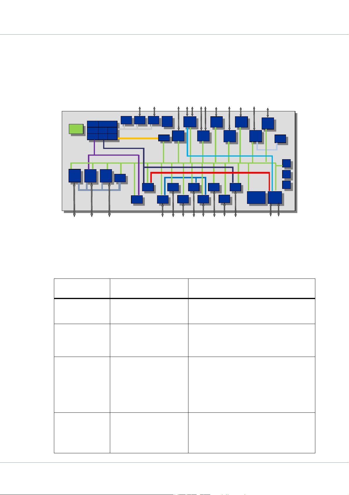
GR716
Onchip
ADC &
DAC
AHBSTAT
I2C
Memory
Controller
RS232
I2C
SPI
1553 A/B
Mil-1553B
BC/RT/MT
SpaceWire
Links
RMAP
CAN
2.0
LVDS /
LVTTL
CAN N/R
DMA
Controller
I/O Port
LEON3FT
SPARC V8
Mul
Trace
64kB
D-ram
FPU
PacketWire
LVDS /
LVTTL
SPI
GPIO
External
ADC &
DAC
PWM
PWM
UART
RS232
Config &
Status
DMA
Controller
Scrub &
ahbstat
AMBA
128kB
I-ram
REX
Memory
Prot
Embeeded
Boot ROM
IrqCtrl &
Timers
Onchip
ADCDAC
SPI2AHB
SPI
I2C2AHB
I2C
SPI4S
SPI
Memory
Controller
PacketWire
Debug Control
Reset /
Clock
Reset /
Watchdog
Clock
BO
POR
BO
LDO
NVRAM
Controller
Ext
ADC
SpacWire
TDP
AHBUART
SPI
Memory
Ext
PROM/SRAM
Memory
NVRAM
Status
and
Control
RS232
WatchDog
Interrupt (Part of AMBA Bus Structure)
TDP
EDAC Errors
EDAC Errors
Scrubber
1553
Reset
Request
PWM
Interrupt, Power-Down, Restart
Memory Protection
AHBSTAT
Debug
(DSU)
Trace
Unit
TRACE
L3STAT
Unit
Serial
Debug
Link
2.2.12 Internal communication
Triggers, events and synchronization signals that require immediate response are distributed outside
the internal AMBA bus structure. This section explains the different connections next to the internal
AMBA structure.
Signal connections are visually shown in figure 3 and described in table 6 in this section.
Figure 3. Internal communication paths outside AMBA bus structure
Table 6. Internal communication paths outside the AMBA bus structure
Connecting functional
Internal bus name
EDAC Error AMBA status, local instruc-
EDAC Error Scrubber
blocks Description
Connection for monitoring of correctable errors
tion memory and local data
memory
AMBA status functionality
in scrubber, external memory controller and NVRAM
signaled from the internal data and instruction
memory.
Connection for monitoring of correctable errors
signaled from the memory controller and
NVRAM controller.
controller
Interrupt Bus All blocks connected to the
Memory protection Protection unit, external
internal AMBA structure
memory controller,
NVRAM controller, local
instruction memory and
local data memory
GR716-DS-UM, May 2019, Version 1.29 26 www.cobham.com/gaisler
Connection for distributing events from/to all
peripherals and digital functionality. The inter-
nal interrupt bus distributes all 64 unique inter-
rupts IDs in table 29. The interrupt bus is used
to program event driven functions e.g. the
DMA channel 0 to respond to a specific Inter-
rupt ID in table 29.
Connection for blocking write access to pro-
tected areas. Protection unit grants or denies
the ongoing AMBA access via the memory
protection bus.
Page 25

GR716
Table 6. Internal communication paths outside the AMBA bus structure
Connecting functional
Internal bus name
Processor Interrupt, Power Down
and Restart
blocks Description
LEON3FT, Interrupt controller and Primary Clock
gating unit.
The interrupts generated on the interrupt bus
are all forwarded to the interrupt controller.
The interrupt controller prioritizes, masks and
propagates the interrupt with the highest prior-
ity to the processor. This bus is also used for
request for Power-Down of the processor and
restart of the processor. Power down request
from the processor is described in section
16.2.16 and reboot is described in section
40.2.7.
Watch Dog Timer unit 0 and reset
request logic
Watch dog timer unit drives a watchdog signal
on this bus to request restart of the system.
Watch dog functionality is described in section
35. User can override reset request with control
register described in section 7.3.
1553 Reset Request MIL-1553 peripheral inter-
faces and reset request logic
MIL-1553B codec request for reset of MIL-
1553B interface support.
TDP MIL-1553B and SpaceWire Internal bus for communication between the
SpaceWire Time Distribution Protocol core and
the SpaceWire interface or the MIL-1553B
interface. For more information see section 34.
DSU DSU and LEON3FT Debug interface for direct access and control of
the LEON3FT processor from debug interface.
PWM PWM, GPIO, DAC and
ADC
PWM synchronization tick outputs. Ticks or
events can be programmed individually for
each PWM to be generated at PWM compare
points, PWM period match, or not generated at
all. PWM ticks are distributed in the system to
synchronize events to the PWM output.
L3STAT To LEON3 Statistical Unit Connection for counting events in the system
defined in table 558 under section "
tion specific events
from REQ/GNT signals
" and in section "Events generated
". Bus is only passively lis-
Implementa-
tening.
TRACE From AMBA infrastructure
to Trace buffer
Main and DMA AMBA buses are routed to the
trace buffer. Trace buffer is passively listening
to signals.
GR716-DS-UM, May 2019, Version 1.29 27 www.cobham.com/gaisler
Page 26
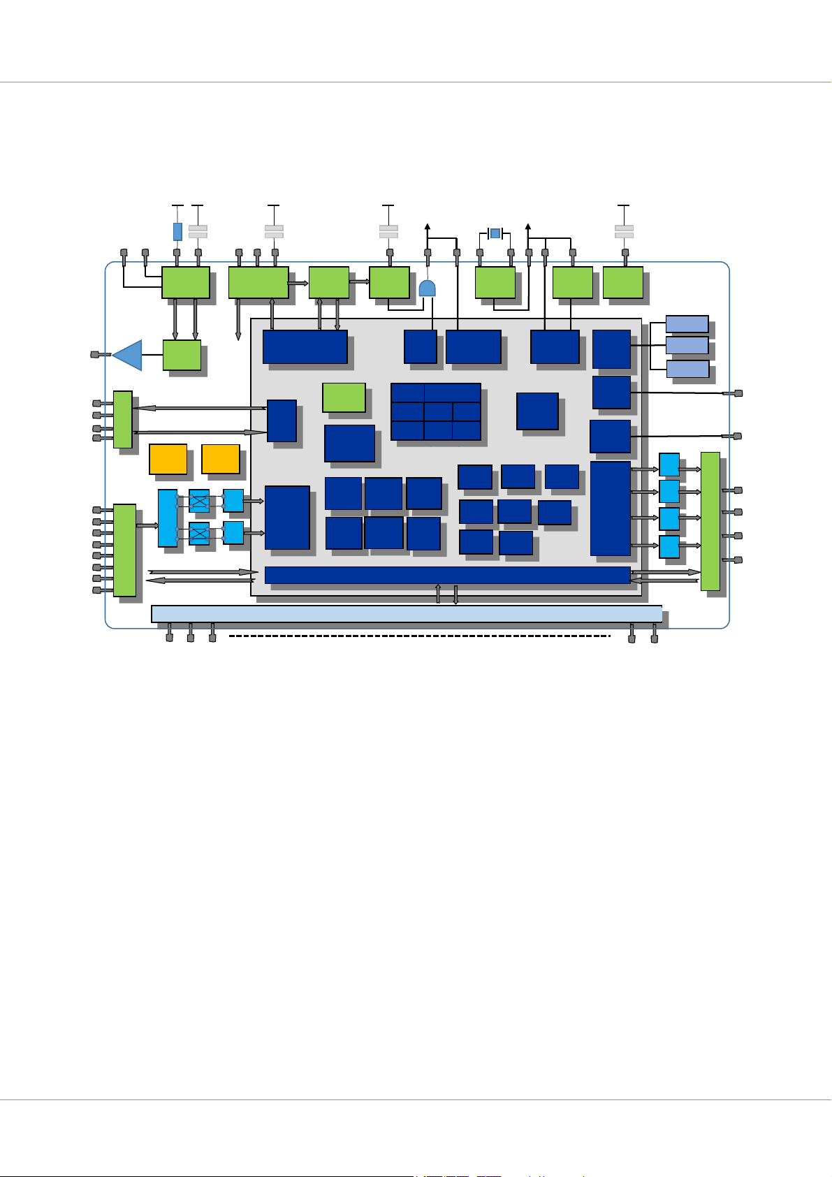
GR716
Memory
Controller
Mil-1553B
BC/RT/MT
SpaceWire
Links
RMAP
CAN
2.0
PacketWire
DMA
Controller
Scrub &
ahbstat
LEON3FT
SPARC V8
Mul
Trace
64kB
D-ram
FPU
AMBA
128kB
I-ram
REX
Memory
Prot
Embeeded
Boot ROM
IrqCtrl &
Timers
UART
SPI4S
BandGap
Ref
LVDS
BO POR XO PLL LDO
(PLL)
Mixed GPIO
MUX
ADC
ADC
LDO
(Core)
Control &
Status
LVDS
MUX
Clock Logic
Onchip
ADCDAC
Digital Mux Logic
Onchip
ADCDAC
Mixed GPIO
Digital GPIO
WDT
Logic
Reset
Logic
Debug
SPIM
Temp
Sensor
Core
Voltage
Sence
Internal
Ref
gen
VREF
Rref
5.11Kohm
C_1v8V
3.3V Supply
1.8V Supply
C_RST
C_PLL
Ext Reset
(RESET_OUT_N)
Ext Clock
Ext Xtal
4Mhz – 25Mhz
DAC DAC DAC DAC
FLASH
ROM
SRAM
NVRAM
I2C
PWM
SPI
GPIO
AMBA
Infrastructure
IntRST_N
Int Vref
Int Iref
Vref
4.7nF
VDDA_REF
VSSA_REF
VDD_CORE
VSSA_PLL
GND_COREVSSA_REF
Vrefbuf
2.3 Analog Architecture Overview
The analog/mixed and power-supply IP blocks are presented here. In figure 4, a simplified block diagram shows these blocks and their analog and power interconnections in the GR716 microcontroller.
Figure 4. Simplified block diagram of the analog/mixed and power-supply IPs in the GR716 microcontroller.
Generally, note that when the XO-oscillator and PLL are used to generate the GR716 microcontroller
clocks, these two blocks must be correctly connected and configured to obtain correct digital functionality of the GR716 microcontroller. Moreover, to obtain correct analog functionality of the GR716
microcontroller, the voltage and current references, set by Vref and Rref, must be correctly connected
and configured, since they provide the GR716 microcontroller with the internal references and bias
currents required by several other IPs in Figure 4.
2.3.1 Reset and Brownout-detector
The RESET and Brownout-detector blocks supervise the supply voltages as shown in Figure 4. The
RESET block provides reset of the internal GR716 microcontroller logic. The internal reset signal,
IntRST_N, is available externally as a 3.3V CMOS output, RESET_OUT_N. The IntRST_N and
RESET_OUT_N signals are low when VDD_CORE is too low. There is also a reset release delay at
power up, starting to count when VDD_CORE goes above its reset threshold level. The Brownout
detectors are intended to be used as pre-warnings to the GR716 microcontroller that some supply voltage(s) has started to go down, so the CPU can perform a well-controlled system shutdown before any
reset detectors are activated. The Brownout detectors are implemented as one detector block on each
supply to be supervised, and each of them has a programmable threshold level that can be set individually. Each Brownout-detector output signal can be programmed by an interrupt mask bit to generate
an interrupt, and typically, the interrupt routine can be used to shut down the system in a controlled
way.
GR716-DS-UM, May 2019, Version 1.29 28 www.cobham.com/gaisler
Page 27

GR716
2.3.2 XO oscillator
The oscillator (XO) is supplied by the LEON3FT microcontroller core voltage, VDD_CORE (1.8V).
The oscillator output is a 3.3V CMOS output and is available on an external pin.
2.3.3 PLL
The PLL is supplied by 1.8V from an internal LDO, which should have an external decoupling capacitor on the PLL supply pin (1.8V). This supply pin shall be left open, with exception of this decoupling capacitor. The PLL provides several internal clock outputs, typically used as clock for the
SpaceWire interface, etc. The PLL reference-clock input is a 3.3V CMOS input, to which the XOoscillator clock output can be directly connected, or any other clock signal generated on PCB fulfilling the electrical specification of this input. The PLL reference-clock input is allowed to be asynchronous to any other clocks in the GR716 microcontroller.
2.3.4 Voltage reference
The reference blocks are supplied by VDDA_REF. This supply needs to have the best voltage integrity on the chip. Therefore, no fast load-current steps are present in any of the on-chip blocks using
this supply. It is essential that especially this supply has good PCB decoupling/filtering (across
VDDA_REF and VSSA_REF) in order to not feed external disturbances from PCB supplies into this
supply. The analog internal references are generated in two steps. First, a reference voltage is generated by an on-chip band-gap reference, which should have an external decoupling capacitor on the
VREF pin. Alternatively, the on-chip reference block can be turned off; then, an external reference
voltage must be applied to this pin (including the right decoupling capacitance needed in that voltagereference implementation). Second, this reference voltage is buffered and put out on the VREFBUF
pin. This reference voltage is also used by an internal current generator, which puts this voltage across
an external reference resistor, RREF on PCB, to generate a precision reference current. Since this reference current is used to generate both the current reference to each DAC and the internal bias cur-
rents required by several other on-chip blocks, RREF can not be chosen arbitrarily to get any desired
DAC full-scale value; it shall be 5.11kohm (or 4.64kohm + 464ohm).
GR716-DS-UM, May 2019, Version 1.29 29 www.cobham.com/gaisler
Page 28

GR716
2.3.5 On-chip ADC
There are two independent ADC blocks. Each ADC is a 11bit/200kSps SAR converter, and has an
analog MUX in-front of it, which means that one MUX channel at a time can be measured. The ADC
can be programmed to single-ended 11-bit range (0 - VREF) using one input pin per channel, or to
differential-input 11-bit range (-VREF to VREF) using two input pins per channel. In-between the
ADC and MUX, there is a fully differential pre-amplifier, which has three programmable gain-settings (x1, x2, x4). It is to be used together with the fully-differential ADC setting. The input impedance is in the order of 5-20 kohm (TBC) when the pre-amplifier is in use. The pre-amplifier can be bypassed by programming; then, the DC input impedance is high (dominated by MUX leakage currents). These three blocks are supplied by VDDA_ADC and VSSA_ADC. This supply is not the analog reference for ADC measurements; however, it must still be really well decoupled/filtered at high
frequencies (>~1MHz) to not degrade the ADC performance.
The ADC supply ground, VSSA_ADC, must always be hardwired to the same PCB ground point as
VSSA_REF, directly outside the Microcontroller package. Otherwise, the ADC measurement range
will be incorrect, since the reference voltage from the on-chip band-gap reference is a single-ended
signal referred to VSSA_REF, whereas the reference input of the on-chip ADC is a single-ended input
referred to VSSA_ADC.
2.3.6 On-chip DAC
There are four independent 12bit/3MSps DAC blocks. The DAC output is a sourcing-current singleended output, typically to be loaded by virtual ground generated by an op-amp on PCB, or by a passive impedance connected to PCB ground providing the output voltage directly across this impedance.
These four DAC blocks are supplied by VDDA_DAC and VSSA_DAC. In the same way as for the
ADC, it is enough to provide really good decoupling/filtering at high frequencies (>~1MHz).
2.3.7 LDO
The LDO provides VDD_CORE with a regulated 1.8V, and needs a 3.3V input supply. The LDO can
be by-passed and, then, the VDD_CORE pins are directly fed with 1.8V regulated supply voltage
from PCB. In this case, the 3.3V LDO input pins must not be connected to any low-impedance node
other than VDD_CORE; one other possibility is to leave the LDO input pins open (non-connected),
but the recommendation is to connect them directly to VDD_CORE. In any case, all VDD_CORE
pins must be decoupled on PCB with a small capacitor (in the order of 10nF) directly at each
VDD_CORE/GND pin pair. When in use, the LDO is always capable of supplying the full maximum
current consumption needed by VDD_CORE. However, the LDO will cause additional on-chip power
dissipation - the core average current times the LDO voltage drop - which will further increase the
junction temperature. Therefore, when running the core logic such that the core current is high, it is
critical to carefully check that the maximum allowed junction temperature is never exceeded in the
thermal situation at hand. This should of course be checked in all application implementations with
the GR716 microcontroller, but is especially important to do carefully when the LDO is in use at the
same time as core current can be high.
GR716-DS-UM, May 2019, Version 1.29 30 www.cobham.com/gaisler
Page 29

GR716
2.3.8 Temperature Sensor
There is a temperature sensor implemented on the GR716 microcontroller chip. Its output signal is a
monotonic voltage versus temperature, and is measured by the on-chip ADC in the same way as any
other MUX channel. Its output is not threshold detected or used in any other on-chip block, so if a
chip over-temperature protection is desired, the user needs to measure the sensor and take adequate
actions in the system application at hand.
2.3.9 Core Voltage (VDD_CORE) Monitor
The core voltage level can be monitored via the on-chip ADC. The voltage measured can be used by
the application to trim the core voltage when the on-chip LDO is active. Default Core voltage trim
value is to have maximum core voltage to always guarantee functionality in worst case corners at
maximum supported clock frequency. For low power applications the core voltage can be decreased
to optimum level in order to minimize power consumption.
GR716-DS-UM, May 2019, Version 1.29 31 www.cobham.com/gaisler
Page 30
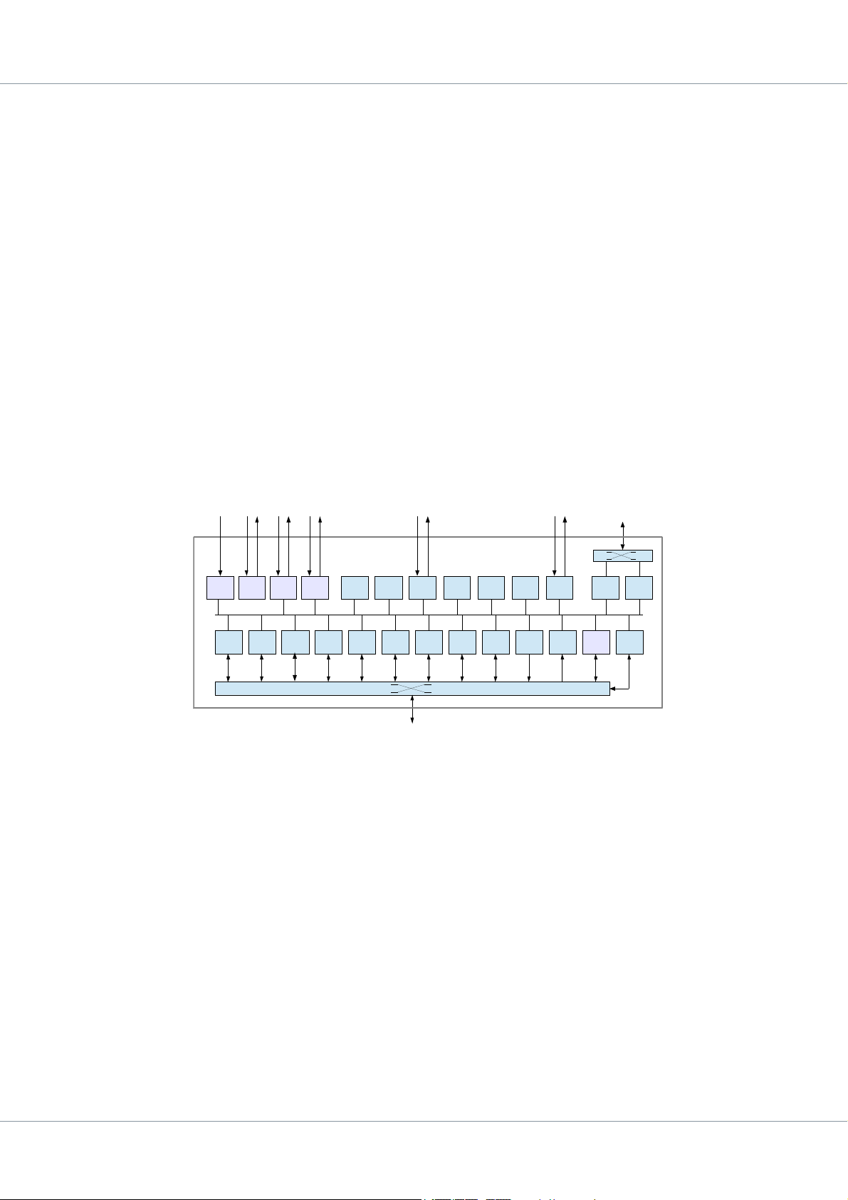
GR716
MCTRL SPI UART ADCDAC I2C GPIO SPW CAN PWRX PW TX1553B
OnChip
ADCDAC
GPREG
Mixed Signal General Puropse
Inputs and outputs
SPW
SPI
For S pac e
LVD S fo r
SpaceWire or
SPI-for-Space
192K RAM
SPI Boot
ROM
IRQ TIMERSLDO
POR
& BO
PLL LSTAT DSULEON3XO
Power
supply
Oscillato r
Power
Sense
and
reset
SpaceWire
clock and
PLL status
DSU
enable,
break and
statu s
External
SPI Boot
ROM
2.4 Signal Overview
The GR716 microcontroller has 64 external general purpose user input and outputs, 6 LVDS transceivers and dedicated SPI memory interface. Almost all 64 external inputs and outputs and LVDS
transceivers have multiple functionality. Functionality is selected by the application software during
startup and configuration. During startup i.e. after reset all user input and outputs are configured as
inputs.
LVDS transmitters are disabled after reset and only enabled if SpaceWire or SPI for Space is enabled.
2.5 I/O switch matrix overview
This section provides a introduction to the I/O switch matrix and gives a presentation to the predefined set of pin configuration.
The I/O switch matrix provides access to several I/O units. When an interface is not activated, its pins
automatically become general purpose I/O. After reset, all I/O switch matrix pins are defined as inputs
until programmed otherwise. Configuration and assigning of functions to external I/O is flexible and
is controlled by software via registers described in section 7.1.
Figure 5 shows an overview of how the various I/O units are connected to the I/O switch matrix.
Figure 5.
Architectural block diagram showing connections to the I/O switch matrix
Table 2.6 shows a listing of all external CMOS pins in the I/O switch matrix and what functions can
be assign to external pins. Table 2.6 also shows configuration registers to assign specific function or
pin to external I/O. To assign a specific function or pin to an external interface the “column” value
should be written into the table ’row’ I/O configuration register and bit field. E.g. n register
SYS.CFG.GP0.GP5 described in section 7.1.
GR716-DS-UM, May 2019, Version 1.29 32 www.cobham.com/gaisler
Page 31

GR716-DS-UM, May 2019, Version 1.29 33 www.cobham.com/gaisler
Table 7. IO configuration option table 1
0x0 0x1 0x2 0x3 0x4 0x5 0x6 0x7 0x8 0x9 0xA 0xB 0xC 0xD 0xE
GPIO0 UART_RTSN0 MEM_ADDR0 1553_RXENA PWRX_BUSYN CAN_TX0 SPIM_SLV1 ADC-DAC_A0 PWM0
GPIO1 UART_CTNS0 MEM_ADDR1 1553_TXA PWRX_CLK CAN_RX0 SPIM_SCK1 ADCDAC_A1 PWM1
GPIO2 UART_TX0 MEM_ADDR2 1553_RXA PWRX_DATA CAN_SEL0 I2CM_SDA0 SPIM_MOSI1 ADCDAC_A2 PWM2
GPIO3 UART_RX0 MEM_ADDR3 1553_RXNA PWRX_ABORT CAN_RX1 I2CM_SCL0 SPIM_MISO1 ADCDAC_A3 PWM3
GPIO4 UART_CTSN1 MEM_ADDR4 1553_TXNA PWRX_VALID CAN_TX1 I2CM_SDA1 SPI_SCK0 ADCDAC_A4 PWM4
GPIO5 UART_RTSN1 MEM_ADDR5 1553_TXINHA PWRX_RDY CAN_SEL1 I2CM_SCL1 SPI_MISO0 ADCDAC_A5 PWM5
SYS.CFG.GP0
GPIO6 UART_TX1 MEM_ADDR6 1553_RXB PWTX_VALID I2CS_SDA0 SPI_MOSI0 ADCDAC_A6 PWM6
GPIO7 UART_RX1 MEM_ADDR7 1553_RXNB PWTX_CLK I2CS_SCL0 SPI_SEL0 ADCDAC_A7 PWM7
GPIO8 UART_CTSN2 MEM_ADDR8 1553_RXENB PWTX_BUSYN I2CS_SDA1 SPI_SLV0_0 PWM8
GPIO9 UART_RTSN2 MEM_ADDR9 1553_TXB PWTX_READY I2CS_SCL1 SPI_SLV0_1 PWM9
GPIO10 UART_TX2 MEM_ADDR10 1553_CLK PWTX_DATA I2CS_SDA2 SPI_SLV0_2 PWM10
GPIO11 UART_RX2 MEM_ADDR11 1553_TXNB PWTX_ABORT I2CS_SCL2 SP I_SLV0_3 PWM11
GPIO12 MEM_ADDR12 1553_TXINHB PWM12
GPIO13 UART_CTSN3 MEM_ADDR13 CAN_TX0 SPI_SCK1 ADCDAC_D0 PWM13
SYS.CFG.GP1
GPIO14 UART_RTSN3 MEM_ADDR14 CAN_RX0 SPI_MISO1 ADCDAC_D1 PWM14
GPIO15 UART_TX3 MEM_ADDR15 CAN_SEL0 SPI_MOSI1 ADCDAC_D2 PWM15
GPIO16 UART_RX3 MEM_ADDR16 CAN_ RX1 SPI_SEL1 ADCDAC_D3
GPIO17 UART_RTSN4 MEM_ADDR17 CAN_TX1 SPI_SLV1_0 ADCDAC_A0
GPIO18 UART_TX4 MEM_ADDR18 CAN_SEL1 SPI_SLV1_1 ADCDAC_A1
GPIO19 UART_RX4 RAM_CSN0 ADCDAC_D4 TDP_SETET
GPIO20 UART_CTSN4 RAM_CSN1 ADCDAC_D5 TDP_E_ET_I
GPIO21 UART_CTSN5 RAM_CSN2 SPI_SLV1_2 ADCDAC_D6 PWM12 SPW_RXS
SYS.CFG.GP2
GPIO22 UART_RTSN5 RAM_CSN3 SPI_SLV1_3 ADCDAC_D7 PWM13 SPW_RXD
GPIO23 UART_TX5 ROM_CSN0 ADCDAC_D8 PWM14 SPW_TXS
GPIO24 UART_RX5 ROM_CSN1 ADCDAC_D9 PWM15 SPW_TXD
GPIO25 MEM_DATA0 PWRX_VALID I2CM_SDA0 SPI_SCK0 ADCDAC_D10 PWM0
GPIO26 MEM_DATA1 PWRX_CLK I2CM_SCL0 SP I_MISO0 ADCDAC_D11 PWM1
GPIO27 MEM_DATA2 PWRX_DATA I2CM_SDA1 SPI_MOSI0 ADCDAC_D12 PWM2
GPIO28 MEM_DATA3 PWRX_ABORT I2CM_SCL1 SPI_SEL0 ADCDAC_D13 PWM3
GPIO29 MEM_DATA4 PWRX_BUSYN I2CS_SDA0 SPI_SLV0_0 ADCDAC_D14 PWM4
SYS.CFG.GP3
GPIO30 MEM_DATA5 PWRX_RDY I2CS_SCL0 SPI_SLV0_1 ADCDAC_D15 PWM5
GPIO31 MEM_DATA6 PWTX_VALID I2CS_SDA1 SPI_SLV0_2 ADC_RC PWM6
GPIO32 MEM_DATA 7 PWTX_CLK I2CS_SCL1 SPI_SLV0_3 DAC_WR PWM7
GPIO33 UART_CTSN3 MEM_OEN PWTX_BUSYN I2CM_SDA0 ADC _CS PWM8
GPIO34 UART_RTSN3 MEM_WRN PWTX_READY I2CM_SCL0 ADC_RDY PWM9
GPIO35 UART_TX3 ROM_CSN0 PWTX_DATA I2CS_SDA0 ADC_TRIG PWM10 MEM_BRDYN
GPIO36 UART_RX3 ROM_CSN1 PWTX_ABORT I2CS_SCL0 ADCDAC_D6 PWM11 MEM_BEXCN
GPIO37 UART_RTSN4 1553_RXENA PWRX_VALID CAN_TX0 SPI_SLV0_3 ADC0 ADCDAC_D7 PWM0
SYS.CFG.GP4
GPIO38 UART_TX4 1553_TXA PWRX_CLK CAN_RX0 SPI_SLV0_2 ADC1 PWM1
GPIO39 UART_RX4 1553_RXA PWRX_DATA CAN_SEL0 I2CS_SDA1 SP I_SLV0_1 ADC2 PWM2
GR716
Page 32

GR716
GR716-DS-UM, May 2019, Version 1.29 34 www.cobham.com/gaisler
0x0 0x1 0x2 0x3 0x4 0x5 0x6 0x7 0x8 0x9 0xA 0xB 0xC 0xD 0xE
GPIO40 UART_CTSN4 1553_RXNA PWRX_ABORT I2CS_SCL1 SPI_SLV0_0 ADC3 ADC_RCPWM3
GPIO41 UART_CTSN5 RAM_CSN2 1553_TXNA PWRX_BYN CAN _TX0 I2CM_SDA0 SPI_SCK0 ADC4 DAC_WR PWM0
GPIO42 UART_RTSN5 RAM_CSN3 1553_TXINHA P WRX_RDY CAN_RX0 I2CM_SCL0 SPI_MISO0 ADC5 ADC_CS PWM1
GPIO43 UART_TX5 ROM_CSN0 1553_RXB PWTX_VALID CAN_SEL0 I2CS_SDA0 SPI_MOSI0 ADC6 ADC_RDY PWM2
GPIO44 UART_RX5 ROM_CSN1 1553_RXNB PWTX_CLK CAN_RX1 I2CS_SCL0 SPI_SEL0 ADC7 ADC_TRIG PWM3
GPIO45 UART_RX0 1553_RXENB PWTX_BUSYN CAN_RX1 SPI_SLV1_1 DAC0 PWM4
SYS.CFG.GP5
GPIO46 UART_TX0 1553_TXB PWTX_RDY SPI_SLV1_0 DAC1 ADCDAC_D15 PWM5
GPIO47 UART_CTSN0 1553_CLK PWTX_DATA CAN_TX1 I2CM_SDA1 SPI_SCK1 DAC2 ADCDAC_D14 PWM6
GPIO48 UART_RTSN0 1553_TXNB PWTX_ABORT CAN_SEL1 I2CM_SCL1 SPI_MISO1 DAC3 ADCDAC_D13 PWM15
GPIO49 UART_CTSN0 MEM_ADDR19 1553_TXINHB I2CS_SDA2 SPI_MOSI1 ADCDAC_D0 PWM0 SPIM_SLV1 AHBUART_TX TDP_SETET
GPIO50 UART_TX0 MEM_ADDR20 I2CS_SCL2 SPI_SEL1 ADCDA C_D1 PWM1 SPIM_SCK1 AHBUART_RX TDP_E_ET_I
GPIO51 UART_RX0 MEM_ADDR21 1553_RXENA SPI_MOSI1 ADCDAC_D2 PWM2 SPIM_MOSI1 TDP_PULSE0
GPIO52 UART_CTSN1 MEM_ADDR22 1553_TXA PWRX_VALID I2CM_SDA0 SPI_SEL1 ADCDAC_D3 PWM3 SPIM_MISO1 TDP_PULSE1
GPIO53 UART_RTSN1 1553_RXA PWRX_C LK I2CM_SCL0 SPIS_SCK0 ADCDAC_D4 PWM4 SPI4S_SCK0
SYS.CFG.GP6
GPIO54 UART_TX1 1553_RXNA PWRX_DATA I2CM_SDA1 SPIS_MISO0 ADCDAC_D5 PWM5 SPI4S_MISO0
GPIO55 UART_RX1 1553_TXNA PWRX_ABORT I2CM_SCL1 SPIS_MOSI0 ADCDAC_D6 PWM6 SPI4S_MOSI0
GPIO56 UART_CTSN2 1553_TXINHA PWRX_BSYN I2CS_SDA0 SPIS_SLV0 ADCDAC_D7 PWM7 SPI4S_SLV0
GPIO57 UART_RTSN2 1553_RXB PWRX_RDY I2CS_SCL0 SPI_SCK0 ADCDAC_D8 PWM8
GPIO58 UART_TXN2 1553_RXNB PWTX_VALID CAN_TX0 I2CS_SDA1 SPI_MISO0 ADCDAC_D9 PWM9
GPIO59 UART_RXN2 1553_RXENB PWTX_CLK CAN_RX0 I2CS_SCL1 SPI_MOSI0 ADCDAC_D10 P WM10
GPIO60 UART_CTSN3 1553_TXB PWTX_BUSYN CAN_SEL0 I2CS_SDA2 SPI_SEL0 ADCDAC_D11 PWM11 TDP_PULSE2
GPIO61 UART_RXN3 1553_CLK PWTX_RDY CAN_RX1 I2CS_SCL2 SPI_SLV0_0 ADCDAC_D12 PWM12 TDP_PULSE3
SYS.CFG.GP7
GPIO62 UART_TX3 ROM_CSN0 1553_TXNB PWTX_DATA CAN_TX1 SPI_SLV0_1 ADCDAC_A0 PWM13 TDP_PULSE4
GPIO63 UART_RTSN3 ROM_CSN1 1553_TXINHB PWTX_ABORT CAN_SEL1 SPI_SLV0_2 ADCDAC_A1 PWM14 TDP_PULSE5
Page 33

GR716
2.6 I/O switch default configurations for bootstraps
This chapter lists external pin connection for all valid boot strap options.
2.6.1 External pin configuration for SpaceWire remote access
This section describes valid bootstrap configuration for SpaceWire remote access.
Table 8. Remote SpaceWire pin configurations
Pin Name Interface Name Functional description
LVDS_RX[1] RXD SpaceWire receiver data interface
LVDS_RX[2] RXS SpaceWire receiver strobe interface
LVDS_TX[0] TXD SpaceWire transmitter data interface
LVDS_TX[1] TXS SpaceWire transmitter strobe interface
Note 1: Remote SpaceWire interface uses LVDS type interface
2.6.2 External pin configuration for UART remote access
This section describes valid bootstrap configuration for UART remote access.
Table 9. Remote UART access pin configurations
Pin Name Interface Name Functional description
GPIO[49] TX UART transmitter interface
GPIO[50] RX UART receiver interface
Note 1: Interface uses CMOS type interface
2.6.3 External pin configuration for I2C remote access
This section describes valid bootstrap configuration for I2C remote access.
Table 10. Remote I2C access pin configurations
Pin Name Interface Name Functional description
GPIO[49] SDA I2C Serial Data interface
GPIO[50] SCL I2C Serial Clock interface
Note 1: Interface uses CMOS type interface
2.6.4 External pin configuration for SPI remote access
This section describes valid bootstrap configuration for SPI remote access.
Table 11. Remote SPI access pin configurations
Pin Name Interface Name Functional description
GPIO[53] SCK SPI Slave Clock interface
GPIO[54] MISO SPI Master input Slave output interface
GPIO[55] MOSI SPI Master output Slave input interface
GPIO[56] SLV SPI Slave Select interface
Note 1: Interface uses CMOS type interface
GR716-DS-UM, May 2019, Version 1.29 35 www.cobham.com/gaisler
Page 34

GR716
2.6.5 External pin configuration for external SPI boot memory
This section describes valid bootstrap configuration for external SPI memory.
Table 12. SPI memory pin configurations
Pin Name Interface Name Functional description
SPIM_MOSI MOSI SPI Memory master output slave input
SPIM_SCK SCK SPI Memory master clock output
SPIM_SEL SEL SPI Memory slave select output
SPIM_MISO MISO SPI Memory master input slave output
GPIO[2] MOSI Redundant SPI Memory master output slave input
GPIO[1] SCK Redundant SPI Memory master clock output
GPIO[0] SEL Redundant SPI Memory slave select output
GPIO[3] MISO Redundant SPI Memory master input slave output
Note 1: Interface uses CMOS type interface
2.6.6 External pin configuration for external SRAM boot memory
This section describes valid bootstrap configuration for external SRAM.
Table 13. SRAM memory pin configurations
Pin Name Interface Name Functional description
GPIO[0] ADDR[0] Memory address interface
GPIO[1] ADDR[1]
GPIO[2] ADDR[2]
GPIO[3] ADDR[3]
GPIO[4] ADDR[4]
GPIO[5] ADDR[5]
GPIO[6] ADDR[6]
GPIO[7] ADDR[7]
GPIO[8] ADDR[8]
GPIO[9] ADDR[9]
GPIO[10] ADDR[10]
GPIO[11] ADDR[11]
GPIO[12] ADDR[12]
GPIO[13] ADDR[13]
GPIO[14] ADDR[14]
GPIO[15] ADDR[15]
GPIO[16] ADDR[16]
GPIO[17] ADDR[17]
GPIO[18] ADDR[18]
GPIO[33] OEN Output interface
GPIO[34] WRN Writen enable interface
GR716-DS-UM, May 2019, Version 1.29 36 www.cobham.com/gaisler
Page 35
GR716
Table 13. SRAM memory pin configurations
Pin Name Interface Name Functional description
GPIO[25] DATA[0] Data interface
GPIO[26] DATA[1]
GPIO[27] DATA[2]
GPIO[28] DATA[3]
GPIO[29] DATA[4]
GPIO[30] DATA[5]
GPIO[31] DATA[6]
GPIO[32] DATA[7]
GPIO[19] CSN[0] Chip Select
GPIO[20] CSN[1] Redundant Chip Select
Note 1: Interface uses CMOS type interface
2.6.7 External pin configuration for external PROM/FLASH boot memory
This section describes valid bootstrap configuration for external PROM/FLASH.
Table 14. PROM/FLASH memory pin configurations
Pin Name Interface Name Functional description
GPIO[0] ADDR[0] Memory address interface
GPIO[1] ADDR[1]
GPIO[2] ADDR[2]
GPIO[3] ADDR[3]
GPIO[4] ADDR[4]
GPIO[5] ADDR[5]
GPIO[6] ADDR[6]
GPIO[7] ADDR[7]
GPIO[8] ADDR[8]
GPIO[9] ADDR[9]
GPIO[10] ADDR[10]
GPIO[11] ADDR[11]
GPIO[12] ADDR[12]
GPIO[13] ADDR[13]
GPIO[14] ADDR[14]
GPIO[15] ADDR[15]
GPIO[16] ADDR[16]
GPIO[17] ADDR[17]
GPIO[18] ADDR[18]
33 OEN Output interface
34 WRN Writen enable interface
GR716-DS-UM, May 2019, Version 1.29 37 www.cobham.com/gaisler
Page 36
GR716
Table 14. PROM/FLASH memory pin configurations
Pin Name Interface Name Functional description
GPIO[25] DATA[0] Data interface
GPIO[26] DATA[1]
GPIO[27] DATA[2]
GPIO[28] DATA[3]
GPIO[29] DATA[4]
GPIO[30] DATA[5]
GPIO[31] DATA[6]
GPIO[32] DATA[7]
GPIO[35] CSN[0] Chip Select
GPIO[36] CSN[1] Redundant Chip Select
Note 1: Interface uses CMOS type interface
2.6.8 External pin configuration for external I2C boot memory
This section describes valid bootstrap configuration for external I2C memory.
Table 15. I2C memory pin configurations
Pin Name Interface Name Functional description
GPIO[2] SDA I2C Serial Data interface
GPIO[3] SCL I2C Serial Clock interface
GPIO[4] SDA Redundant I2C Serial Data interface
GPIO[5] SCL Redundant I2C Serial Clock interface
Note 1: Interface uses CMOS type interface
2.7 I/O switch matrix options, considerations and limitations
This chapter lists options and limitations when using different interfaces in the IO switch.
2.7.1 SPI interfaces
The SPI interface can switch from being a Master to Slave interface and vice versa. In general this is
not a problem and adds flexibility to the I/O mux concept except for the ’slave select’ signal. The
’slave select’ signal will change direction when switching from Slave i.e. slave select input signal to
Master interface i.e. slave select output. In the worst scenario this can permanently damage the internal driver and receiver. To mitigate this problem the Master Slave select output and Slave Select input
has been assigned to different I/Os.
In a situation where the application board only requires the SPI interface to either be Slave or Master
the option is given to the designer to assign the extra pin to another system interface.
2.7.2 External Memory interface
The external PROM/SRAM interface occupies many external I/Os due parallel data and address
buses. The system should only allocate the number of address and chip-select pins needed for the
application. E.g. a system that only requires 256KiB of memory only need to allocate and use 18
external address lines and 1 chip-select i.e. the system can assign 4 pins to another system interface.
There is also a potential saving to make if the functionality ’bus ready’ and ’bus exception’ isn’t used.
GR716-DS-UM, May 2019, Version 1.29 38 www.cobham.com/gaisler
Page 37

GR716
2.7.3 External ADC and DAC interface
The number of pins used for the external ADC and DAC interface depends upon the number of external ADC and DAC channel the application shall support. The interface can use up to 8 address lines in
order to address and control multiple ADC and DAC outside the GR716 microcontroller. On the other
hand, if very few or only one ADC or DAC is used the 8 address lines can be assigned to another system interface.
2.8 I/O switch matrix pin validation script
This an introduction to the validation script provided upon request in order to validate pin configurations and to generate constants for the I/O switch configuration registers. The intention of the script is
to help the user of the GR716 microcontroller to validate a configuration according to table 2.6 and to
quickly setup a system for test. The script should not be used for any other purpose than test and
debug of systems using the GR716 microcontroller.
2.8.1 Functional pin mapping sections
The I/O configuration script is written in TCL and contains lists for mapping functional pins to physical pins on the GR716 microcontroller as described in table 2.6. Each functional group maps individual functional pins to physical external pins. Example of UART0 configuration description are shown
in table 16.
Table 16. UART0 functional pin mapping to external pins of the GR716 microcontroller
set uart0_cfg0 { {uart0_cfg0} {
{ 1 1 uart_ctsn(0) in}
{ 0 1 uart_rtsn(0) out}
{ 2 1 uart_tx(0) out}
{ 3 1 uart_rx(0) in}
} }
Table 16 specifies the following for the configuration UART0_CFG0:
• functional pin UART_CTSN(0) of UART0 to mapped to external physical pin GPIO(0)
• functional pin UART_RTSN(0) of UART0 to mapped to external physical pin GPIO(1)
• functional pin UART_TX(0) of UART0 to mapped to external physical pin GPIO(2)
• functional pin UART_RX(0) of UART0 to mapped to external physical pin GPIO(3)
Functions can have multiple I/O configurations and are then differentiated by adding a consecutive
number to the name of the configuration. All interface options described in table 2.6 are described in
the I/O mux script.
2.8.2 I/O configuration sections
The I/O configuration section specifies all functional groups to be available on physical pins. The
functions and configurations are listed and named in this section. Example of using UART0, UART1
and UART3 are listed in table 16.
Table 17. Example of mapping UART0, UART1 and UART2 to external pins of the GR716 microcontroller
set iomx_uart0_cfg [list \
$auart_cfg0 $uart2_cfg0 $uart3_cfg1 \
]
GR716-DS-UM, May 2019, Version 1.29 39 www.cobham.com/gaisler
Page 38

GR716
2.8.3 Usage of the pin validation script
Script needs to be modified and loaded into GRMON. After script been loaded the TCL command
gen_config can be run to generate the external I/O configuration register settings.
Table 18. Example of executing I/O configuration script
grmon2> source iomx.tcl
grmon2> gen_config $iomx_uart0_cfg
...
grmon2>
2.8.4 Output of the pin validation script
The I/O script can be executed from within GRMON using the build-in TCL support. Here is an
example of running the script for setting up the system using with SpaceWire, 1 UART and external
SPI memory.
Table 19. Example of output from running the pin validation script when successful
grmon2> source iomx.tcl
grmon2> gen_config $iomx_apw_uart0_spi0_cfg
# Pin list
pin[0]: uart_ctsn(0)
pin[1]: uart_rtsn(0)
pin[2]: uart_tx(0)
pin[3]: uart_rx(0)
pin[12]: spim_sck(0)
pin[13]: spim_miso(0)
pin[14]: spim_mosi(0)
pin[15]: spim_slv(0)
pin[16]: spw_rxd
pin[17]: spw_rxs
pin[18]: spw_txs
pin[19]: spw_txd
// C constant
const int iomx[8] = {
0x00001111,
0x11110000,
0x00002222,
0x00000000,
0x00000000,
0x00000000,
0x00000000,
0x00000000};
grmon2>
GR716-DS-UM, May 2019, Version 1.29 40 www.cobham.com/gaisler
Page 39

GR716
The script outputs:
• A section specifying all pins that are dedicated to specific interface. (All other pins are considered as GPIOs)
• A section that can be imported directly to standard ’C’ program for configuration of I/O mux registers, see section 7.1.
2.8.5 Erroneous pin configuration
Script checks for conflicting pins and a third section will be printed when running the scripts.
Table 20. Example of output from running the pin validation script when conflicting pins are detected
grmon2> source iomx.tcl
...
Error: conflicting pin config
Double-mapped signal:
uart_ctsn(3) uart_rtsn(3) uart_tx(3) uart_rx(3)
grmon2>
The last printed section will print the pins violating the selected pins configuration.
2.8.6 Validation of custom pin configuration
The supplied validation scripts contains variables for valid pin placement of each interface specified
in table 2.6. See script for valid names.
2.8.7 Script limitations
The script is provided "as-is" and only checks for valid configurations according to pre-defined pin
allocations for specific interfaces defined in the script.
The script will not check pins placement or direction selected is correct according to target system or
PCB board.
GR716-DS-UM, May 2019, Version 1.29 41 www.cobham.com/gaisler
Page 40

GR716
2.9 I/O switch matrix scenario examples
This chapter gives examples of how to configure the GR716 microcontroller and the I/O mux for following scenarios:
• Sensor / Actuator Node using external SRAM to store data
• Bus bridge using external SRAM to store data
• Bus bridge booting from external serial ROM
This chapter presents examples of I/O mux configuration tables. The configuration tables e.g. table 22
should be interpreted as follow:
• Each row represent an external I/O on the GR716 microcontroller device
• The first column states the register and bits used to control the external I/O
• The columns marked with a hexadecimal number states the value the function are selected with.
For reference see table
• The columns marked with <namn>.<index> are a combined user scenarios and gives the fixed
functions and pins for the scenario
• Empty entries in columns marked with <namn>.<index> indicates that the user can assign any
valid function to the external pin according to table
2.6.
2.6.
2.9.1 Scenario #1 - Sensor / Actuator Node
This chapter describes how to configure the I/O mux to node bus either via SPW, CAN or MIL-1553B
and at the same run internal or external ADC.
The following assumptions are made for the system:
• All on-chip ADCs and DACs is used (or external ADC / DAC).
• External RAM needs to be greater than 128KiB. (If the application needs less than that the internal on-chip memory should be used in order to utilize the pins on the device more efficiently).
For this example we assume 256KiB is needed.
• Boot from external PROM is required.
In table 21 options of I/O configuration for using SPW, MIL-1553B and CAN as node bus are
depicted. Note that SpaceWire is connected on dedicated pins.
GR716-DS-UM, May 2019, Version 1.29 42 www.cobham.com/gaisler
Page 41

GR716
IO Config Register MIL.CFG1 MIL.CFG2 CAN.CFG1 CAN.CFG2 SPW.CFG1 SPW.CFG2
SYS.CFG.GP0.GP0 MEM_ADDR0 MEM_ADDR0 MEM_ADDR0 MEM_ADDR0 MEM_ADDR0 MEM_ADDR0
SYS.CFG.GP0.GP1 MEM_ADDR1 MEM_ADDR1 MEM_ADDR1 MEM_ADDR1 MEM_ADDR1 MEM_ADDR1
SYS.CFG.GP0.GP2 MEM_ADDR2 MEM_ADDR2 MEM_ADDR2 MEM_ADDR2 MEM_ADDR2 MEM_ADDR2
SYS.CFG.GP0.GP3 MEM_ADDR3 MEM_ADDR3 MEM_ADDR3 MEM_ADDR3 MEM_ADDR3 MEM_ADDR3
SYS.CFG.GP0.GP4 MEM_ADDR4 MEM_ADDR4 MEM_ADDR4 MEM_ADDR4 MEM_ADDR4 MEM_ADDR4
SYS.CFG.GP0.GP5 MEM_ADDR5 MEM_ADDR5 MEM_ADDR5 MEM_ADDR5 MEM_ADDR5 MEM_ADDR5
SYS.CFG.GP0.GP6 MEM_ADDR6 MEM_ADDR6 MEM_ADDR6 MEM_ADDR6 MEM_ADDR6 MEM_ADDR6
SYS.CFG.GP0.GP7 MEM_ADDR7 MEM_ADDR7 MEM_ADDR7 MEM_ADDR7 MEM_ADDR7 MEM_ADDR7
SYS.CFG.GP1.GP0 MEM_ADDR8 MEM_ADDR8 MEM_ADDR8 MEM_ADDR8 MEM_ADDR8 MEM_ADDR8
SYS.CFG.GP1.GP1 MEM_ADDR9 MEM_ADDR9 MEM_ADDR9 MEM_ADDR9 MEM_ADDR9 MEM_ADDR9
SYS.CFG.GP1.GP2 MEM_ADDR10 MEM_ADDR10 MEM_ADDR10 MEM_ADDR10 MEM_ADDR10 MEM_ADDR10
SYS.CFG.GP1.GP3 MEM_ADDR11 MEM_ADDR11 MEM_ADDR11 MEM_ADDR11 MEM_ADDR11 MEM_ADDR11
SYS.CFG.GP1.GP4 MEM_ADDR12 MEM_ADDR12 MEM_ADDR12 MEM_ADDR12 MEM_ADDR12 MEM_ADDR12
SYS.CFG.GP1.GP5 MEM_ADDR13 MEM_ADDR13 MEM_ADDR13 MEM_ADDR13 MEM_ADDR13 MEM_ADDR13
SYS.CFG.GP1.GP6 MEM_ADDR14 MEM_ADDR14 MEM_ADDR14 MEM_ADDR14 MEM_ADDR14 MEM_ADDR14
SYS.CFG.GP1.GP7 MEM_ADDR15 MEM_ADDR15 MEM_ADDR15 MEM_ADDR15 MEM_ADDR15 MEM_ADDR15
SYS.CFG.GP2.GP0 MEM_ADDR16 MEM_ADDR16 MEM_ADDR16 MEM_ADDR16 MEM_ADDR16 MEM_ADDR16
SYS.CFG.GP2.GP1 MEM_ADDR17 ADCDAC_A0 MEM_ADDR17 ADCDAC_A0 MEM_ADDR17 ADCDAC_A0
SYS.CFG.GP2.GP2 MEM_ADDR18 ADCDAC_A1 MEM_ADDR18 ADCDAC_A1 MEM_ADDR18 ADCDAC_A1
SYS.CFG.GP2.GP3 RAM_CSN0 RAM_CSN0 RAM_CSN0 RAM_CSN0 RAM_CSN0 RAM_CSN0
SYS.CFG.GP2.GP4 RAM_CSN1 ADCDAC_D5 RAM_CSN1 RAM_CSN1 RAM_CSN1 RAM_CSN1
SYS.CFG.GP2.GP5 RAM_CSN2 ADCDAC_D6 RAM_CSN2 RAM_CSN2 SPW_RXD
SYS.CFG.GP2.GP6 RAM_CSN3 ADCDAC_D7 RAM_CSN3 RAM_CSN3 SPW_RXS
SYS.CFG.GP2.GP7 ROM_CSN0 ADCDAC_D8 ROM_CSN0 ROM_CSN0 SPW_TXS
SYS.CFG.GP3.GP0 ROM_CSN1 ADCDAC_D9 ROM_CSN1 ROM_CSN1 SPW_TXD
SYS.CFG.GP3.GP1 MEM_DATA0 MEM_DATA0 MEM_DATA0 MEM_DATA0 MEM_DATA0 MEM_DATA0
SYS.CFG.GP3.GP2 MEM_DATA1 MEM_DATA1 MEM_DATA1 MEM_DATA1 MEM_DATA1 MEM_DATA1
SYS.CFG.GP3.GP3 MEM_DATA2 MEM_DATA2 MEM_DATA2 MEM_DATA2 MEM_DATA2 MEM_DATA2
SYS.CFG.GP3.GP4 MEM_DATA3 MEM_DATA3 MEM_DATA3 MEM_DATA3 MEM_DATA3 MEM_DATA3
SYS.CFG.GP3.GP5 MEM_DATA4 MEM_DATA4 MEM_DATA4 MEM_DATA4 MEM_DATA4 MEM_DATA4
SYS.CFG.GP3.GP6 MEM_DATA5 MEM_DATA5 MEM_DATA5 MEM_DATA5 MEM_DATA5 MEM_DATA5
SYS.CFG.GP3.GP7 MEM_DATA6 MEM_DATA6 MEM_DATA6 MEM_DATA6 MEM_DATA6 MEM_DATA6
SYS.CFG.GP4.GP0 MEM_DATA7 MEM_DATA7 MEM_DATA7 MEM_DATA7 MEM_DATA7 MEM_DATA7
SYS.CFG.GP4.GP1 MEM_OEN MEM_OEN MEM_OEN MEM_OEN MEM_OEN MEM_OEN
SYS.CFG.GP4.GP2 MEM_WRN MEM_WRN MEM_WRN MEM_WRN MEM_WRN MEM_WRN
SYS.CFG.GP4.GP3 ROM_CSN0 ROM_CSN0 ROM_CSN0
SYS.CFG.GP4.GP4 ROM_CSN1 ROM_CSN1 ROM_CSN1
SYS.CFG.GP4.GP5 ADC0 1553_RXENA ADC0 CAN_TX0
SYS.CFG.GP4.GP6 ADC1 1553_TXA ADC1 CAN_RX0
SYS.CFG.GP4.GP7 ADC2 1553_RXA ADC2 CAN_SEL0
SYS.CFG.GP5.GP0 ADC3 ADC_RC ADC3 ADC_RC ADC_RC
SYS.CFG.GP5.GP1 ADC4 DAC_WR ADC4 DAC_WR DAC_WR
SYS.CFG.GP5.GP2 ADC5 ADC_CS ADC5 ADC_CS ADC_CS
SYS.CFG.GP5.GP3 ADC6 ADC_RDY ADC6 ADC_RDY ADC_RDY
SYS.CFG.GP5.GP4 ADC7 ADC_TRIG ADC7 ADC_TRIG ADC_TRIG
SYS.CFG.GP5.GP5 DAC0 1553_RXENB DAC0 CAN_RX1
SYS.CFG.GP5.GP6 DAC1 1553_TXB DAC1 ADCDAC_D15 ADCDAC_D15
SYS.CFG.GP5.GP7 DAC2 1553_CLK DAC2 ADCDAC_D14 ADCDAC_D14
SYS.CFG.GP6.GP0 DAC3 ADCDAC_D13 DAC3 ADCDAC_D13 ADCDAC_D13
SYS.CFG.GP6.GP1 ADCDAC_D0 ADCDAC_D0 ADCDAC_D0
SYS.CFG.GP6.GP2 ADCDAC_D1 ADCDAC_D1 ADCDAC_D1
SYS.CFG.GP6.GP3 1553_RXENA ADCDAC_D2 ADCDAC_D2 ADCDAC_D2
SYS.CFG.GP6.GP4 1553_TXA ADCDAC_D3 ADCDAC_D3 ADCDAC_D3
SYS.CFG.GP6.GP5 1553_RXA ADCDAC_D4 ADCDAC_D4 ADCDAC_D4
SYS.CFG.GP6.GP6 1553_RXNA 1553_RXNA ADCDAC_D5 ADCDAC_D5
SYS.CFG.GP6.GP7 1553_TXNA 1553_TXNA ADCDAC_D6 ADCDAC_D6
SYS.CFG.GP7.GP0 1553_TXINHA 1553_TXINHA ADCDAC_D7 ADCDAC_D7
SYS.CFG.GP7.GP1 1553_RXB 1553_RXB ADCDAC_D8 ADCDAC_D8
SYS.CFG.GP7.GP2 1553_RXNB 1553_RXNB CAN_TX0 ADCDAC_D9 ADCDAC_D9
SYS.CFG.GP7.GP3 1553_RXENB ADCDAC_D10 CAN_RX0 ADCDAC_D10 ADCDAC_D10
SYS.CFG.GP7.GP4 1553_TXB ADCDAC_D11 CAN_SEL0 ADCDAC_D11 ADCDAC_D11
SYS.CFG.GP7.GP5 1553_CLK ADCDAC_D12 CAN_RX1 ADCDAC_D12 ADCDAC_D12
SYS.CFG.GP7.GP6 1553_TXNB 1553_TXNB CAN_TX1 CAN_TX1
SYS.CFG.GP7.GP7 1553_TXINHB 1553_TXINHB CAN_SEL1 CAN_SEL1
MIL1553 CAN SpaceWire
Table 21. Examples of I/O configuration for using SPW, MIL-1553B and CAN as node bus
GR716-DS-UM, May 2019, Version 1.29 43 www.cobham.com/gaisler
Page 42

GR716
2.9.2 Scenario #2 - Bus bridge
This chapter describes how to configure the I/O mux for a node bus bridge.
The following assumptions are made for the system:
• External RAM needs to be greater than 128KiB. (If the application needs less than that the internal on-chip memory should be used in order to utilize the pins on the device more efficiently).
For this example we assume at least 256KiB is needed.
• Boot from external PROM is required.
• Connects to spacecraft bus either via 1553B or SpaceWire, and on the other side to node bus via
CAN.
In table 22 two example of I/O configurations for Node bus bridge are shown.
Note that SpaceWire is assumed to be connected on dedicated pins see BRIDGE.CFG1 in table 22. If
SpaceWire redundancy is required configuration BRIDGE.CFG2 in table 22 should be used.
GR716-DS-UM, May 2019, Version 1.29 44 www.cobham.com/gaisler
Page 43
GR716
IO Config Register BRIDGE.CFG1 BRIDGE.CFG2
SYS.CFG.GP0.GP0 MEM_ADDR0 MEM_ADDR0
SYS.CFG.GP0.GP1 MEM_ADDR1 MEM_ADDR1
SYS.CFG.GP0.GP2 MEM_ADDR2 MEM_ADDR2
SYS.CFG.GP0.GP3 MEM_ADDR3 MEM_ADDR3
SYS.CFG.GP0.GP4 MEM_ADDR4 MEM_ADDR4
SYS.CFG.GP0.GP5 MEM_ADDR5 MEM_ADDR5
SYS.CFG.GP0.GP6 MEM_ADDR6 MEM_ADDR6
SYS.CFG.GP0.GP7 MEM_ADDR7 MEM_ADDR7
SYS.CFG.GP1.GP0 MEM_ADDR8 MEM_ADDR8
SYS.CFG.GP1.GP1 MEM_ADDR9 MEM_ADDR9
SYS.CFG.GP1.GP2 MEM_ADDR10 MEM_ADDR10
SYS.CFG.GP1.GP3 MEM_ADDR11 MEM_ADDR11
SYS.CFG.GP1.GP4 MEM_ADDR12 MEM_ADDR12
SYS.CFG.GP1.GP5 MEM_ADDR13 MEM_ADDR13
SYS.CFG.GP1.GP6 MEM_ADDR14 MEM_ADDR14
SYS.CFG.GP1.GP7 MEM_ADDR15 MEM_ADDR15
SYS.CFG.GP2.GP0 MEM_ADDR16 MEM_ADDR16
SYS.CFG.GP2.GP1 MEM_ADDR17 MEM_ADDR17
SYS.CFG.GP2.GP2 MEM_ADDR18 MEM_ADDR18
SYS.CFG.GP2.GP3 RAM_CSN0 RAM_CSN0
SYS.CFG.GP2.GP4 RAM_CSN1 RAM_CSN1
SYS.CFG.GP2.GP5 RAM_CSN2 SPW_RXD
SYS.CFG.GP2.GP6 RAM_CSN3 SPW_RXS
SYS.CFG.GP2.GP7 ROM_CSN0 SPW_TXS
SYS.CFG.GP3.GP0 ROM_CSN1 SPW_TXD
SYS.CFG.GP3.GP1 MEM_DATA0 MEM_DATA0
SYS.CFG.GP3.GP2 MEM_DATA1 MEM_DATA1
SYS.CFG.GP3.GP3 MEM_DATA2 MEM_DATA2
SYS.CFG.GP3.GP4 MEM_DATA3 MEM_DATA3
SYS.CFG.GP3.GP5 MEM_DATA4 MEM_DATA4
SYS.CFG.GP3.GP6 MEM_DATA5 MEM_DATA5
SYS.CFG.GP3.GP7 MEM_DATA6 MEM_DATA6
SYS.CFG.GP4.GP0 MEM_DATA7 MEM_DATA7
SYS.CFG.GP4.GP1 MEM_OEN MEM_OEN
SYS.CFG.GP4.GP2 MEM_WRN MEM_WRN
SYS.CFG.GP4.GP3 ROM_CSN0
SYS.CFG.GP4.GP4 ROM_CSN1
SYS.CFG.GP4.GP5 1553_RXENA 1553_RXENA
SYS.CFG.GP4.GP6 1553_TXA 1553_TXA
SYS.CFG.GP4.GP7 1553_RXA 1553_RXA
SYS.CFG.GP5.GP0 1553_RXNA 1553_RXNA
SYS.CFG.GP5.GP1 1553_TXNA 1553_TXNA
SYS.CFG.GP5.GP2 1553_TXINHA 1553_TXINHA
SYS.CFG.GP5.GP3 1553_RXB 1553_RXB
SYS.CFG.GP5.GP4 1553_RXNB 1553_RXNB
SYS.CFG.GP5.GP5 1553_RXENB 1553_RXENB
SYS.CFG.GP5.GP6 1553_TXB 1553_TXB
SYS.CFG.GP5.GP7 1553_CLK 1553_CLK
SYS.CFG.GP6.GP0 1553_TXNB 1553_TXNB
SYS.CFG.GP6.GP1 1553_TXINHB 1553_TXINHB
SYS.CFG.GP6.GP2
SYS.CFG.GP6.GP3
SYS.CFG.GP6.GP4
SYS.CFG.GP6.GP5
SYS.CFG.GP6.GP6
SYS.CFG.GP6.GP7
SYS.CFG.GP7.GP0
SYS.CFG.GP7.GP1
SYS.CFG.GP7.GP2 CAN_TX0 CAN_TX0
SYS.CFG.GP7.GP3 CAN_RX0 CAN_RX0
SYS.CFG.GP7.GP4 CAN_SEL0 CAN_SEL0
SYS.CFG.GP7.GP5 CAN_RX1 CAN_RX1
SYS.CFG.GP7.GP6 CAN_TX1 CAN_TX1
SYS.CFG.GP7.GP7 CAN_SEL1 CAN_SEL1
Bridge
Table 22. Examples of I/O MUX configurations for Node bus bridges when using the external parallel memory
GR716-DS-UM, May 2019, Version 1.29 45 www.cobham.com/gaisler
Page 44

GR716
2.9.3 Scenario #3 - Bus bridge booting from external serial ROM
This chapter shows how to make use of more I/O and describes how to configure the I/O mux for a
node bus bridge.
The following assumptions are made for the system:
• System boots and runs software from external serial memory. (Software can also execute from
internal instruction memory).
• Connects to spacecraft bus either via MIL-1553B or SpaceWire, and on the other side to node
bus via CAN.
In table 23 two example of I/O configurations for Node bus bridge are depicted. Note that the external
SPI configuration ROM and SpaceWire are connected on dedicated pins.
GR716-DS-UM, May 2019, Version 1.29 46 www.cobham.com/gaisler
Page 45

GR716
IO Config Register BRIDGE.CFG1 BRIDGE.CFG2
SYS.CFG.GP0.GP0
SYS.CFG.GP0.GP1
SYS.CFG.GP0.GP2
SYS.CFG.GP0.GP3
SYS.CFG.GP0.GP4
SYS.CFG.GP0.GP5
SYS.CFG.GP0.GP6
SYS.CFG.GP0.GP7
SYS.CFG.GP1.GP0
SYS.CFG.GP1.GP1
SYS.CFG.GP1.GP2
SYS.CFG.GP1.GP3
SYS.CFG.GP1.GP4
SYS.CFG.GP1.GP5
SYS.CFG.GP1.GP6
SYS.CFG.GP1.GP7
SYS.CFG.GP2.GP0
SYS.CFG.GP2.GP1
SYS.CFG.GP2.GP2
SYS.CFG.GP2.GP3
SYS.CFG.GP2.GP4
SYS.CFG.GP2.GP5 SPW_RXD
SYS.CFG.GP2.GP6 SPW_RXS
SYS.CFG.GP2.GP7 SPW_TXS
SYS.CFG.GP3.GP0 SPW_TXD
SYS.CFG.GP3.GP1
SYS.CFG.GP3.GP2
SYS.CFG.GP3.GP3
SYS.CFG.GP3.GP4
SYS.CFG.GP3.GP5
SYS.CFG.GP3.GP6
SYS.CFG.GP3.GP7
SYS.CFG.GP4.GP0
SYS.CFG.GP4.GP1
SYS.CFG.GP4.GP2
SYS.CFG.GP4.GP3
SYS.CFG.GP4.GP4
SYS.CFG.GP4.GP5 1553_RXENA 1553_RXENA
SYS.CFG.GP4.GP6 1553_TXA 1553_TXA
SYS.CFG.GP4.GP7 1553_RXA 1553_RXA
SYS.CFG.GP5.GP0 1553_RXNA 1553_RXNA
SYS.CFG.GP5.GP1 1553_TXNA 1553_TXNA
SYS.CFG.GP5.GP2 1553_TXINHA 1553_TXINHA
SYS.CFG.GP5.GP3 1553_RXB 1553_RXB
SYS.CFG.GP5.GP4 1553_RXNB 1553_RXNB
SYS.CFG.GP5.GP5 1553_RXENB 1553_RXENB
SYS.CFG.GP5.GP6 1553_TXB 1553_TXB
SYS.CFG.GP5.GP7 1553_CLK 1553_CLK
SYS.CFG.GP6.GP0 1553_TXNB 1553_TXNB
SYS.CFG.GP6.GP1 1553_TXINHB 1553_TXINHB
SYS.CFG.GP6.GP2
SYS.CFG.GP6.GP3
SYS.CFG.GP6.GP4
SYS.CFG.GP6.GP5
SYS.CFG.GP6.GP6
SYS.CFG.GP6.GP7
SYS.CFG.GP7.GP0
SYS.CFG.GP7.GP1
SYS.CFG.GP7.GP2 CAN_TX0 CAN_TX0
SYS.CFG.GP7.GP3 CAN_RX0 CAN_RX0
SYS.CFG.GP7.GP4 CAN_SEL0 CAN_SEL0
SYS.CFG.GP7.GP5 CAN_RX1 CAN_RX1
SYS.CFG.GP7.GP6 CAN_TX1 CAN_TX1
SYS.CFG.GP7.GP7 CAN_SEL1 CAN_SEL1
Bridge
Table 23. Examples of I/O MUX configurations for Node bus bridges when using the external serial memory
GR716-DS-UM, May 2019, Version 1.29 47 www.cobham.com/gaisler
Page 46

GR716
2.10 Cores
The design is based on the following cores from the GRLIB IP Library:
Table 24. Used IP cores
Core Function Vendor Device
AHB2AHB Bi-directional AHB/AHB bridge 0x01 0x020
AHBROM Generic AHB ROM 0x01 0x1B
AHBSTAT AHB Status Register 0x01 0x052
AHBTRACE AHB trace buffer 0x01 0x017
AHBUART Serial/AHB Debug interface 0x01 0x007
APBCTRL AHB/APB bridge 0x01 0x006
APBUART 8-bit UART with FIFO 0x01 0x00C
DSU3 LEON3 Debug Support Unit 0x01 0x004
LRAM Local on-chip SRAM with EDAC and AHB interface 0x01 0x0A3
FTMCTRL 8/16/32-bit memory controller with EDAC 0x01 0x054
GPTIMER Modular timer unit with watchdog 0x01 0x038
GR1553B MIL-STD-1553B / AS15531 interface 0x01 0x04D
GRADCDAC ADC/DAC Interface 0x01 0x036
GRCAN CAN 2.0 controller with DMA 0x01 0x03D
GRCLKGATE Clock gating unit 0x01 0x02C
GRDMAC DMA Controller with internal AHB/APB bridge 0x01 0x095
GRGPIO General Purpose I/O Port 0x01 0x01A
GRGPIO_SEQ General Purpose Sequencer 0x01 0x1F8
GRGPREG General purpose register 0x01 0x087
GRMEMPROT Memory protection 0x01 0x1F1
GRPWM PWM controller 0x01 0x04A
GRPWRX PacketWire receiver 0x01 0x08D
GRPWTX PacketWire transmitter 0x01 0x08E
GRSPW2 SpaceWire codec with AHB host interface and RMAP 0x01 0x029
I2C2AHB I2C to AHB bridge 0x01 0x00B
I2CMST I2C master 0x01 0x028
I2CSLV I2C slave 0x01 0x03E
IRQ(A)MP Multiprocessor interrupt controller with AMP extensions 0x01 0x00D
L3STAT LEON3 statistical unit 0x01 0x098
LEON3FT LEON3 SPARC V8 32-bit processor 0x01 0x053
MEMSCRUB Memory scrubber 0x01 0x057
RSTGEN Reset generator N/A N/A
SPI2AHB SPI to AHB bridge 0x01 0x05C
SPICTRL SPI controller 0x01 0x02D
SPIMCTRL SPI memory controller 0x01 0x045
SPISLAVE SPI for space slave 0x01 0x0A7
The information in the last two columns is available via plug’n’play information in the system and is
used by software to detect peripherals and to initialize software drivers.
GR716-DS-UM, May 2019, Version 1.29 48 www.cobham.com/gaisler
Page 47

GR716
2.11 Memory map
The memory map of the internal AHB and APB buses as seen from the processor cores can be seen
below.
The column ’DMA Access’ in the Memory map table indicates if the AMBA peripheral is accessible
by a DMA controller.
Table 25. AMBA memory map, as seen from processors
Core Address range Area
AHBROM 0x00000000 - 0x000FFFFF Internal Boot PROM Yes
FTMCTRL 0x01000000 - 0x01FFFFFF External PROM Yes
SPIMCTRL 0x02000000 - 0x03FFFFFF SPI Memory 0 mapped area Yes
SPIMCTRL 0x04000000 - 0x05FFFFFF SPI Memory 1 mapped area Yes
DLRAM 0x30000000 - 0x300FFFFF Processor local data memory Yes
ILRAM 0x31000000 - 0x310FFFFF Processor local instruction memory Yes
FTMCTRL 0x40000000 - 0x4FFFFFFF External SRAM Memory Yes
NVRAM 0x50000000 - 0x50FFFFFF Reserved space for internal NVRAM Yes
A
P
B
B
C
T
R
L
0
DMA
Access
FTMCTRL 0x80000000 - 0x800000FF Memory controller with EDAC No
DLRAM 0x80001000 - 0x800010FF On-chip Data memory control registers No
IRQAMP 0x80002000 - 0x800023FF Multi-processor Interrupt Ctrl. No
GPTIMER 0x80003000 - 0x800030FF Modular Timer Unit 0 with Watchdog support No
GPTIMER 0x80004000 - 0x800040FF Modular Timer Unit 1 No
MEMPROT 0x80005000 - 0x800051FF Memory Protection Unit for system bus No
GRCLKGATE 0x80006000 - 0x800060FF Clock gating configuration register unit 0 No
GRCLKGATE 0x80007000 - 0x800070FF Clock gating configuration register unit 1 No
GRGPREG 0x80008000 - 0x800080FF Configuration and test registers No
L3STAT 0x80009000 - 0x800093FF LEON3 Statistics Unit No
AHBSTAT 0x8000A000 - 0x8000A0FF AHB Status Register for DMA AMBA bus No
ILRAM 0x8000B000 - 0x8000B0FF On-chip Instruction memory control registers No
GRSPWTDP 0x8000C000 - 0x8000C1FF CCSDS TDP / SpaceWire I/F No
GRGPRBANK 0x8000D000 - 0x8000D0FF IO Mux configuration register No
GRGPREG 0x8000E000 - 0x8000E0FF Test register and system control register No
AHBUART 0x8000F000 - 0x8000F0FF Slave UART configuration for remote access No
GR716-DS-UM, May 2019, Version 1.29 49 www.cobham.com/gaisler
Page 48

GR716
Table 25. AMBA memory map, as seen from processors
Core Address range Area
GRSPW2 0x80100000 - 0x801000FF GRSPW2 SpaceWire Serial Link No
GR1553B 0x80101000 - 0x801010FF MIL-STD-1553B Interface No
GRCAN 0x80102000 - 0x801023FF CAN Controller with DMA No
A
GRCAN 0x80103000 - 0x801033FF CAN Controller with DMA No
P
SPI2AHB 0x80104000 - 0x801040FF SPI to AHB Bridge No
B
I2C2AHB 0x80105000 - 0x801050FF I2C to AHB Bridge No
C
GRDMAC 0x80106000 - 0x801061FF Stand alone DMA unit 0 No
T
GRDMAC 0x80107000 - 0x801071FF Stand alone DMA unit 1 No
R
GRDMAC 0x80108000 - 0x801081FF Stand alone DMA unit 2 No
L
GRDMAC 0x80109000 - 0x801091FF Stand alone DMA unit 3 No
1
MEMPROT 0x8010A000 - 0x8010A0FF Memory protection for DMA bus No
BANDGAP 0x8010B000 - 0x8010B0FF Bandgap control registers No
BO 0x8010C000 - 0x8010C0FF Brown-Out detection control registers No
PLL 0x8010D000 - 0x8010D0FF PLL control registers No
PWRX 0x8010E000 - 0x8010E0FF PacketWire Receiver with DMA No
PWTX 0x8010F000 - 0x8010F0FF PacketWire Transmitter with DMA No
APBUART
APBUART
APBUART
A
APBUART
P
APBUART
B
APBUART
C
T
AHBSTAT
R
NVRAM
L
GRADCDAC
2
SPICTRL
SPICTRL
1)
1)
1)
1)
1)
1)
1)
1)
1)
1)
0x80300000 - 0x803000FF Generic UART 0 Yes
0x80301000 - 0x803010FF Generic UART 1 Yes
0x80302000 - 0x803020FF Generic UART 2 Yes
0x80303000 - 0x803030FF Generic UART 3 Yes
0x80304000 - 0x803040FF Generic UART 4 Yes
0x80305000 - 0x803050FF Generic UART 5 Yes
0x80306000 - 0x803060FF AHB Status Register for MAIN AMBA bus Yes
0x80307000 - 0x803070FF Memory controller with EDAC (NVRAM) Yes
1)
0x80308000 - 0x803080FF External ADC / DAC Interface Yes
0x80309000 - 0x803090FF SPI Controller 0 Yes
0x8030A000 - 0x8030A0FF SPI Controller 1 Yes
0x8030B000 - 0x8030BFFF Unused -
GRGPIO
GRGPIO
I2CMST
I2CMST
GRPWM0
1)
1)
1)
1)
1)
0x8030C000 - 0x8030CFFF General Purpose I/O port 0 to 31 Yes
0x8030D000 - 0x8030DFFF General Purpose I/O port 32 to 64 Yes
0x8030E000 - 0x8030E0FF I2C-master 0 Yes
0x8030F000 - 0x8030F0FF I2C-master 1 Yes
0x80310000 - 0x803100FF PWM generator 0 Yes
DMA
Access
GR716-DS-UM, May 2019, Version 1.29 50 www.cobham.com/gaisler
Page 49

GR716
Table 25. AMBA memory map, as seen from processors
Core Address range Area
A
P
B
C
T
R
L
3
1)
ADC
1)
ADC
1)
ADC
1)
ADC
1)
ADC
1)
ADC
1)
ADC
1)
ADC
1)
DAC
1)
DAC
1)
DAC
1)
DAC
I2CSLV
I2CSLV
GRSPI4
1)
1)
1)
GRPWM1
1)
0x80400000 - 0x804000FF On-chip ADC interface 0 Yes
0x80401000 - 0x804010FF On-chip ADC interface 1 Yes
0x80402000 - 0x804020FF On-chip ADC interface 2 Yes
0x80403000 - 0x804030FF On-chip ADC interface 3 Yes
0x80404000 - 0x804040FF On-chip ADC interface 4 Yes
0x80405000 - 0x804050FF On-chip ADC interface 5 Yes
0x80406000 - 0x804060FF On-chip ADC interface 6 Yes
0x80407000 - 0x804070FF On-chip ADC interface 7 Yes
0x80408000 - 0x804080FF On-chip DAC interface 0 Yes
0x80409000 - 0x804090FF On-chip DAC interface 1 Yes
0x8040A000 - 0x8040A0FF On-chip DAC interface 2 Yes
0x8040B000 - 0x8040B0FF On-chip DAC interface 3 Yes
0x8040C000 - 0x8040C0FF I2C-slave 0 Yes
0x8040D000 - 0x8040D0FF I2C-slave 1 Yes
0x8040E000 - 0x8040E0FF SPI for Space Slave Yes
0x80410000 - 0x804100FF PWM generator 1 Yes
DMA
Access
GR716-DS-UM, May 2019, Version 1.29 51 www.cobham.com/gaisler
Page 50

GR716
*(DEST_ADDR + ATOMIC_OP_OFFSET) = ATOMIC_MASK;
Table 25. AMBA memory map, as seen from processors
Core Address range Area
AHBUART 0x94000000 - 0x940000FF AHB Debug UART Yes
L3STAT 0x94001000 - 0x940013FF LEON3 Statistics Unit Yes
GRGPREG 0x94002000 - 0x940020FF Analog test control Yes
A
P
B
C
T
R
L
D
B
G
DSU3 0x90000000 - 0x907FFFFF LEON3 Debug Support Unit Yes
- 0x94000000 - 0x940FFFFF APB bus DBG address space Yes
AHBTRACE1 0x9ff20000 - 0x9ff3FFFF AHB Trace Buffer Yes
- 0x9FFFF000 - 0x9FFFFFFF Configuration area for Debug bus Yes
MEMSCRUB 0xFFF00000 - 0xFFF000FF Memory scrubber registers Yes
SPIMCTRL 0xFFF00100 - 0xFFF001FF SPIMCTRL control registers 0 Yes
SPIMCTRL 0xFFF00200 - 0xFFF002FF SPIMCTRL control registers 1 Yes
- 0xFFFFF000 - 0xFFFFFFFF Configuration area for system main bus Yes
0x94003000 - 0x94003FFF Unused -
0x94004000 - 0x94004FFF Unused -
0x94005000 - 0x94005FFF Unused -
0x94006000 - 0x94006FFF Unused --
0x94007000 - 0x94007FFF Unused -
0x94008000 - 0x94008FFF Unused -
0x94009000 - 0x94009FFF Unused -
0x9400A000 - 0x9400AFFF Unused -
0x9400B000 - 0x9400BFFF Unused -
0x9400C000 - 0x9400CFFF Unused -
0x9400D000 - 0x9400DFFF Unused -
0x9400E000 - 0x9400EFFF Unused -
0x9400F000 - 0x9400FFFF Unused -
DMA
Access
Note 1: CPU and DMA controller accesses specified memory areas using different APB interfaces. The
Accesses to unused AMBA AHB address space will result in an AMBA ERROR response, this
applies to the memory areas that are marked as "Unused" in the table above. Accesses to unused areas
located on one of the AHB/APB bridges will not have any effect, note that these unoccupied address
ranges are not marked as "Unused" in the table above. No AMBA ERROR response will be given for
memory allocated to one of the APB bridges.
2.12 Atomic access
This chapter describes how atomic read and modify operations are performed in the GR716 microcontroller. The GR716 microcontroller supports atomic read-modify-write operations in hardware by
mirroring the address space of the peripheral and internal data memory for different atomic operations. Atomic operations supported are OR, AND, XOR and Set&Clear.
Atomic operations are performed by adding an atomic operation offset to the destination register
address of the normal write operation of a atomic bit mask:
Table 26.
For atomic operations in local processor data memory
CPU and DMA can access different APB peripherals at the same time without conflict
GR716-DS-UM, May 2019, Version 1.29 52 www.cobham.com/gaisler
Page 51

GR716
(ADDR + OP) & 0xFFFFF000) + ((ADDR & 0x00000FFF) << 1)
Local data memory use the following atomic offset:
• OR operation offset: 0x10000
• AND operation offset 0x20000
• XOR operation offset 0x30000
• Set and clear operation offset: 0x40000
APB peripheral registers use the following atomic of
fset:
• AND operation offset: 0x20000
• OR operation offset 0x40000
• XOR operation offset 0x60000
• Set and clear operation offset: 0x80000
When using the atomic set and clear function, some extra precautio
ns have to be taken. In order to be
able to both set and clear a 32 bit register two consecutive 32-bit writes need to be performed. The
access will not be executed and an error response will be given if a non-related access appears in
between the 2 writes to the same slave. To guarantee no non-related access in between the 2 atomic set
and clear write accesses the LEON3FT processors ability to perform a double store should be used.
[SPARC]
All addresses in the atomic set and clear address space have been aligned to 0x8 i.e. local write
address in processor data memory or APB peripheral needs to be modified in order to avoid exception
from the LEON3FT processor. The shifted address is automatically decoded in the local memory or
the APB peripheral.
Table 27. Set and clear atomic operation address definition
For simplicity and to guarantee the use of a double store it is recommended to include a function that
forces the usage of the double store operation. An example of such a function for using atomic set and
clear function to register in APB peripherals is included in this chapter:
Table 28. Example of Atomic set and clear function using SPARC V8 double store operation
// Atomic set and clear for aliging write address and setting operation offset
// function need set and clear mask and address to peripheral
void SetAndClear (unsigned int _set, unsigned int _clr, unsigned int *addr)
{
unsigned long long a = ((unsigned long long int) _set << 32) | _clr; // Concatenate set and clear
unsigned int b = (unsigned int)addr & 0xFFFFF000; // Keep base address
b += 0x80000; // Add atomic offset for op.
b |= (((unsigned int) addr & 0x00000FFF) << 1); // Align local address to 0x8
__asm__ volatile ("std %1, [%0]"::"r"(b),"r"(a)); // Insert double store op
}
// mask
GR716-DS-UM, May 2019, Version 1.29 53 www.cobham.com/gaisler
Page 52

GR716
2.13 Interrupts
The table below indicates the interrupt default assignments. All interrupts are handled by the interrupt
controller and forwarded to the LEON3 processors. For more configuration and option see chapter
Table 29. Bus Interrupt line assignments
Interrupt ID Interrupt Line Core Comment
0 n/a not used
1 1 Extended Extended Interrupts for primary interrupt controller
2 2 GRPWRX Interrupt from PacketWire RX controller
3 3 GRPWTX Interrupt from PacketWire TX controller
4 4 GR1553 Interrupt from GR1553 controller
5 5 GRSPW2 Interrupt from SpaceWire controller
6 6 GRDMAC DMA controller interrupt 0 - 3
7 7 I2CS/2AHB/SPI2AHB Interrupt from I2C Slave 0 and 1 / I2C2AHB / SPI2AHB
8 8 GRPWM Interrupt from PWM controller
9 9 GPTIMER0 Interrupt 1 from timer block 0
10 10 GPTIMER0 Interrupt 2 from timer block 0
11 11 GPTIMER0 Interrupt 3 from timer block 0
12 12 GPTIMER0 Interrupt 4 from timer block 0
13 13 GPTIMER0 Interrupt 5 from timer block 0
14 14 GPTIMER0 Interrupt 6 from timer block 0
15 15 GPTIMER0 Interrupt 7 from timer block 0 (WDOG)
40
16 16 GRADCDAC External ADC interface
17 17 GRGPIO Interrupt from GPIO controller 0 / External DAC
18 18 GRGPIO (Interrupt from GPIO controller 0)
19 19 GRGPIO (Interrupt from GPIO controller 0)
20 20 GRGPIO (Interrupt from GPIO controller 0)
21 21 GRCAN0&1 Interrupt from CAN controller
22 22 GRCAN0&1 Interrupt from CAN RX controller
23 23 GRCAN0&1 Interrupt from CAN TX controller
24 24 APBUART APBUART interface interrupt 0
25 25 APBUART APBUART interface interrupt 1
26 26 DAC on-chip DAC 0 interrupt
27 27 DAC on-chip DAC 1 interrupt
28 28 ADC0 on-chip ADC interrupt 0
29 29 ADC1 on-chip ADC interrupt 1
30 30 ADC2 on-chip ADC interrupt 2
31 31 ADC3 on-chip ADC interrupt 3
28 32 ADC4 on-chip ADC interrupt 4
29 33 ADC5 on-chip ADC interrupt 5
30 34 ADC6 on-chip ADC interrupt 6
GR716-DS-UM, May 2019, Version 1.29 54 www.cobham.com/gaisler
Page 53

GR716
Table 29. Bus Interrupt line assignments
Interrupt ID Interrupt Line Core Comment
31 35 ADC7 on-chip ADC interrupt 7
26 36 DAC on-chip DAC 2 interrupt
27 37 DAC on-chip DAC 3 interrupt
16 38 GRGPIO Interrupt from GPIO controller 1
17 39 GRGPIO (Interrupt from GPIO controller 1)
18 40 GRGPIO (Interrupt from GPIO controller 1)
19 41 GRGPIO (Interrupt from GPIO controller 1)
3 42 APBUART APBUART interface interrupt 2
443GRSPWTDPSpaceWire TDP
5 44 APBUART APBUART interface interrupt 3
6 45 APBUART APBUART interface interrupt 4
7 46 APBUART APBUART interface interrupt 5
8 47 I2CSLV1 / I2C2AHB I2C Slave Interface 0 and/or I2C2AHB
11 48 SPICTRL Interrupt from SPI controller 0
12 49 SPICTRL Interrupt from SPI controller 1
13 50 I2CM Interrupt from I2C master controller 0
14 51 I2CM Interrupt from I2C master controller 1
2 52 SPIMCTRL Interrupt from SPI memory controller 0 and 1
20 53 GPTIMER1 Interrupt 1 from timer block 1
21 54 GPTIMER1 Interrupt 2 from timer block 1
22 55 GPTIMER1 Interrupt 3 from timer block 1
23 56 GPTIMER1 Interrupt 4 from timer block 1
24 57 GPTIMER1 Interrupt 5 from timer block 1
25 58 GPTIMER1 Interrupt 6 from timer block 1
26 59 GPTIMER1 Interrupt 7 from timer block 1
16 60 GRGPIOSEQ0 GPIO sequencer 0
17 61 GRGPIOSEQ1 GPIO sequencer 1
18 62 PLL PLL interrupt, Power On Reset and Brown Out interrupt
19 63 AHBSTAT/DLRAM,
ILRAM/GRGPRBANK/
MEMSCRUB
AHB status, Scrubbers and I/O mux interrupt
GR716-DS-UM, May 2019, Version 1.29 55 www.cobham.com/gaisler
Page 54

GR716
3 Signals
3.1 Bootstrap signals
The power-up and initialisation state is affected by several external signals as shown in table 30.The
bootstrap signals taken via GPIO, DUART and SPIM signals are saved when the on-chip system reset
is released. This occurs after deassertion of the internal power-on-reset or RESET_IN_N input and
valid input clock on the SYS_CLK pin. The state of the signals are sampled and stored in a bootstrap
register. See section 7.2 for boot strap register description.
Note that some pins used for bootstrapping have dual purpose can be used for normal operations after
reset has been released.
Table 30. Bootstrap signals
Pin Functional description
DSU_EN Enables the Debug Support Unit (DSU) and other members connected to the Debug AHB bus. If
DSU_BREAK Puts processor in debug mode when asserted while DSU_EN is HIGH. When DSU_EN is LOW,
GPIO[17] Enable bypass of internal boot ROM.
GPIO[0] Determines the use of EDAC for external boot RAM when the GR716 microcontroller shall boot from
GPIO[62] Enable test of internal memories at startup. The processor starts checking internal memory for bit errors
GPIO[63] Enables extra protection of external boot source or setting SpaceWire clock frequency
DUART_TXD If boot from external SRAM/ROM/SPI-ROM this pin are used for selecting to copy ASW image from
SPIM_MOSI Enable remote access. When remote access is disabled processor will start from selected external boot
DSU_EN is HIGH the DSU and the Debug AHB bus will be clocked. If DSU_EN is LOW the DSU
and all members on the Debug AHB bus will be clock gated off
BREAK is assigned to the timer enable bit of the watchdog timer and also controls if the processor
starts executing after reset.
Boot strapping this signal 'high' will force the processor NOT to execute the internal boot software.
Normally the processor starts executing from address 0x0. But if this bootstrap is 'high' the processor
will start execute from software from address selected by bootstrap signals SPIM_MOSI & SPIM_SCK
& SPIM_SEL.
external memory. Set to low for enabling EDAC and to high for disabling EDAC.
Determine the use of PLL when the GR716 microcontroller shall boot via a remote source.
during boot if this bootstrap is set to 'high'. Setting this to 'high' will slow down the boot processes since
the check is software based.
If boot from external RAM/ROM this pin enable the use of redundant memory if primary boot memory
fails.
If remote access via SPW this pin together with DUART_TXD are used to set the SpaceWire default
speed.
selected external boot RAM/ROM (If not set for this option. The GR716 microcontroller will start execute from the selected external memory)
If remote access via SPW is selected this pin together with GPIO[63] are used to set the SPW default
speed. Set DUART_TXD & GPIO[63] accordingly depending on external SpaceWire frequency:
"00" - For 5Mhz external frequency source
"01" - For 10Mhz external frequency source
"10" - For 20Mhz external frequency source
"11" - For 25Mhz external frequency source
memory.
GR716-DS-UM, May 2019, Version 1.29 56 www.cobham.com/gaisler
Page 55

GR716
Table 30. Bootstrap signals
Pin Functional description
SPIM_SCK &
SPIM_SEL
Note 1: User should use weak pull-up/pull-downs for configuration of the GR716 microcontroller. A weak
Note 2: Bootstrap signals determine state of GR716 microcontroller after reset has been released.
Note 3: The LEON3FT processor is always enabled after reset has been released.
Note 4: Remote access request will force the processor to power down according to 16.2.16 after initialization
Note 5: Remote access will enable clocks according to table:
Note 6: Only requested memory interface will have clock and pins enabled.
Note 7: Watchdog timer will always be enabled and not controllable from bootstraps.
This pin together with the pin SPIM_MOSI selects which source the LEON3FT microcontroller should
boot from:
When copy ASW boot from external source is selected (SPIM_MOSI is low)
"00" - Copy software image from SPI Memory
"01" - Copy software image from external SRAM
"10" - Copy software image from external ROM
"11" - Copy software image from external I2C
When boot from external source is selected (SPIM_MOSI is low)
"00" - Boot from SPI Memory
"01" - Boot from external SRAM
"10" - Boot from external ROM
"11" - Unused
Enable for remote access interfaces (SPIM_MOSI is high)
"00" - SPI remote access
"01" - SpaceWire RMAP enable
"10" - I2C remote access
"11" - UART remote access
resistor is defined as resistor which require low current from the drive circuitry. The resistance should
be greater or equal to 10K ohm.
has been completed.
1. SpaceWire option will enable SpaceWire core and external SpaceWire interface
2. SPI option will enable SPI for Space Slave and external SPI for Space interface
3. I2C option will enable I2C2AHB bridge and external I2C interface
4. UART option will enable AHBUART1 and external UART interface
GR716-DS-UM, May 2019, Version 1.29 57 www.cobham.com/gaisler
Page 56

GR716
3.1.1 Boot strap configuration for remote access
This section describes valid bootstrap configuration for remote access:
Table 31. Remote bootstrap configurations
Pin
Remote Access Source Space Wire Divisor PLL
SPIM_MOSI SPIM_SCK SPIM_SEL DUART_TXD GPIO[63] GPIO[0] GPIO[17] GPIO[62]
4) 5)
Boot Bypass Memory test
Functional description
high low high low low low low low Enable SpaceWire
remote access using a 5
MHz input clock after
initialization of the processor
high low high low low low low high Enable SpaceWire
remote access using a 5
MHz input clock after
initialization of the processor and internal memory test.
high low high low high low low low Enable SpaceWire
remote access using a 10
MHz input clock after
initialization of the processor
high low high low high low low high Enable SpaceWire
remote access using a 10
MHz input clock after
initialization of the processor and internal memory test.
high low high high low low low low Enable SpaceWire
remote access using a 20
MHz input clock after
initialization of the processor
high low high high low low low high Enable SpaceWire
remote access using a 20
MHz input clock after
initialization of the processor and internal memory test.
high low high high low low low low Enable SpaceWire
remote access using a 25
MHz input clock after
initialization of the processor
high low high high low low low high Enable SpaceWire
remote access using a 25
MHz input clock after
initialization of the processor and internal memory test.
high low high
2)
x
2)
x
high low low Enable SpaceWire
remote access using the
clock direct from the
SpaceWire input pin after
initialization of the processor
GR716-DS-UM, May 2019, Version 1.29 58 www.cobham.com/gaisler
Page 57

GR716
Table 31. Remote bootstrap configurations
Pin
Remote Access Source Space Wire Divisor PLL
SPIM_MOSI SPIM_SCK SPIM_SEL DUART_TXD GPIO[63] GPIO[0] GPIO[17] GPIO[62]
high low high
2)
x
2)
x
4) 5)
Boot Bypass Memory test
Functional description
high low high Enable SpaceWire
remote access using the
clock direct from the
SpaceWire input pin after
initialization of the processor and internal memory test.
high low low
2)
x
2)
x
2)
x
low low Enable SPI remote
access after initialization
of the processor.
high low low
2)
x
2)
x
2)
x
low high Enable SPI remote
access after initialization
of the processor and
internal memory test.
high high low
2)
x
2)
x
2)
x
low low Enable I2C remote
access after initialization
of the processor.
high high low
2)
x
2)
x
2)
x
low high Enable I2C remote
access after initialization
of the processor and
internal memory test.
high high high
2)
x
2)
x
2)
x
low low Enable UART remote
access after initialization
of the processor.
high high high
2)
x
2)
x
2)
x
low high Enable UART remote
access after initialization
of the processor and
internal memory test.
Note 1: To enable remote access SPIM_MOSI must be bootstrapped to high.
Note 2: Configuration pin has no effect or not used for bootstrap configuration. It recommend to tie the pin to either
low or high.
Note 3: Processor are forced into power down mode after processor and memory test has been completed.
Note 4: Enable internal PLL by bootstrap signal to low. When using the internal PLL the link speed will be set to 10
Mbps after reset and maximum link speed after auto negotiation of link speed is 100 Mbps.
Note 5: Disable internal PLL by bootstrap signal to high. When bypassing the internal PLL the speed will be set to
input frequency of the SpaceWire clock. The PLL will be in power down mode.
GR716-DS-UM, May 2019, Version 1.29 59 www.cobham.com/gaisler
Page 58

GR716
3.1.2 Boot strap configuration for external SPI memory
This section describes valid bootstrap configuration for use of external memory options:
Table 32. External SPI memory bootstrap configurations
Pin
Red
4)
EDAC
5)
Bypass
6)
Memory test
Functional description
5)
low
7)
Enable external SPI
Remote Access Source ASW
SPIM_MOSI SPIM_SCK SPIM_SEL DUART_TXD GPIO[63] GPIO[0] GPIO[17] GPIO[62]
3)
low low low low low
memory boot. Processor
will start execute application software direct
from memory after initialization of the processor.
low low low low low
5)
high
7)
Enable external SPI
memory boot. Processor
will start execute application software direct
from memory.
low low low high low
5)
low low Enable external ASW
SPI memory boot after
initialization of the processor. Processor will
copy and extract ASW
container before executing application software.
low low low high high
5)
low low Enable external ASW
SPI memory with DMR
protection boot after initialization of the processor. Processor will copy
and extract ASW container before executing
application software.
Note 1: To enable external memory access SPIM_MOSI must be bootstrapped to low.
Note 2: Configuration pin has no effect or not used for bootstrap configuration. It recommend to tie the pin either to
low or high.
Note 3: Enable ASW protection. ASW protection usage is described in section 51.
Note 4: Enable dual module redundancy protection. Option only valid in combination with ASW protection. Redun-
dant memory is expected to located at 0x04000000.
Note 5: Enable BCH EDAC protection. EDAC can be enabled and used in combination with all other options. When
configuration is used external memory must included BCH check bits.
Note 6: Enable bypass of the internal boot ROM. When enabled the processor will start execute code directly from
the primary memory at 0x02000000. Processor or internal memory is initialized after reset when this option
is used.
Note 7: Enable memory test. Memory test configuration can be used in combination with all other options. Memory
test have no affect when internal boot ROM is bypassed.
GR716-DS-UM, May 2019, Version 1.29 60 www.cobham.com/gaisler
Page 59

GR716
3.1.3 Boot strap configuration for external SRAM memory
This section describes valid bootstrap configuration for use of external memory options:
Table 33. External SRAM memory bootstrap configurations
Pin
Red
4)
EDAC
5)
Bypass
6)
Memory test
Functional description
5)
low
7)
Enable external SRAM
Remote Access Source ASW
SPIM_MOSI SPIM_SCK SPIM_SEL DUART_TXD GPIO[63] GPIO[0] GPIO[17] GPIO[62]
3)
low low high low low
memory boot. Processor
will start execute application software direct
from memory after initialization of the processor.
low low high low low
5)
high
7)
Enable external SRAM
memory boot. Processor
will start execute application software direct
from memory.
low low high high low
5)
low low Enable external ASW
SRAM memory boot
after initialization of the
processor. Processor will
copy and extract ASW
container before executing application software.
low low high high high
5)
low low Enable external ASW
SRAM memory with
DMR protection boot
after initialization of the
processor. Processor will
copy and extract ASW
container before executing application software.
Note 1: To enable external memory access SPIM_MOSI must be bootstrapped to low.
Note 2: Configuration pin has no effect or not used for bootstrap configuration. It recommend to tie the pin either to
low or high.
Note 3: Enable ASW protection. ASW protection usage is described in section 51.
Note 4: Enable dual module redundancy protection. Option only valid in combination with ASW protection. Redun-
dant memory is expected to located at TBD.
Note 5: Enable BCH EDAC protection. EDAC can be enabled and used in combination with all other options. When
configuration is used external memory must included BCH check bits.
Note 6: Enable bypass of the internal boot ROM. When enabled the processor will start execute code directly from
the primary memory at 0x40000000. Processor or internal memory is initialized after reset when this option
is used.
Note 7: Enable memory test. Memory test configuration can be used in combination with all other options. Memory
test have no affect when internal boot ROM is bypassed.
GR716-DS-UM, May 2019, Version 1.29 61 www.cobham.com/gaisler
Page 60

GR716
3.1.4 Boot strap configuration for external PROM/FLASH memory
This section describes valid bootstrap configuration for use of external memory options:
Table 34. External PROM/FLASH memory bootstrap configurations
Pin
Red
4)
EDAC
5)
Bypass
6)
Memory test
Functional description
5)
low
7)
Enable external PROM/
Remote Access Source ASW
SPIM_MOSI SPIM_SCK SPIM_SEL DUART_TXD GPIO[63] GPIO[0] GPIO[17] GPIO[62]
3)
low high low low low
FLASH memory boot.
Processor will start execute application software direct from memory
after initialization of the
processor.
low high low low low
5)
high
7)
Enable external PROM/
FLASH memory boot.
Processor will start execute application software direct from
memory.
low high low high low
5)
low low Enable external ASW
PROM/FLASH memory
boot after initialization of
the processor. Processor
will copy and extract
ASW container before
executing application
software.
low high low high high
5)
low low Enable external ASW
PROM/FLASH memory
with DMR protection
boot after initialization of
the processor. Processor
will copy and extract
ASW container before
executing application
software.
Note 1: To enable external memory access SPIM_MOSI must be bootstrapped to low
Note 2: Configuration pin has no effect or not used for bootstrap configuration. It recommend to tie the pin either to
low or high.
Note 3: Enable ASW protection. ASW protection usage is described in section 51.
Note 4: Enable dual module redundancy protection. Option only valid in combination with ASW protection. Redun-
dant memory is expected to located at TBD.
Note 5: Enable BCH EDAC protection. EDAC can be enabled and used in combination with all other options. When
configuration is used external memory must included BCH check bits.
Note 6: Enable bypass of the internal boot ROM. When enabled the processor will start execute code directly from
the primary memory at 0x01000000. Processor or internal memory is initialized after reset when this option
is used.
Note 7: Enable memory test. Memory test configuration can be used in combination with all other options. Memory
test have no affect when internal boot ROM is bypassed.
GR716-DS-UM, May 2019, Version 1.29 62 www.cobham.com/gaisler
Page 61

GR716
3.1.5 Boot strap configuration for external I2C memory
This section describes valid bootstrap configuration for use of external memory options:
Table 35. External SPI memory bootstrap configurations
Pin
Red
4)
EDAC
5)
Bypass
6)
Memory test
Functional description
5)
low
7)
Enable external ASW
Remote Access Source ASW
SPIM_MOSI SPIM_SCK SPIM_SEL DUART_TXD GPIO[63] GPIO[0] GPIO[17] GPIO[62]
3)
low high high high low
I2C memory boot after
initialization of the processor. Processor will
copy and extract ASW
container before executing application software.
low high high high high
5)
low
7)
Enable external ASW
I2C memory with DMR
protection boot after initialization of the processor. Processor will copy
and extract ASW container before executing
application software.
Note 1: To enable external memory access SPIM_MOSI must be bootstrapped to low
Note 2: Configuration pin has no effect or not used for bootstrap configuration. It recommend to tie the pin either to
low or high.
Note 3: Enable ASW protection. ASW protection usage is described in section 51.
Note 4: Enable dual module redundancy protection. Option only valid in combination with ASW protection. Redun-
dant memory is expected to located at I2C master unit 1.
Note 5: Configuration pin has no effect or not used for bootstrap configuration. It recommend to tie the pin either to
low or high.
Note 6: Bypass boot ROM must always be strapped to low when I2C option is used.
Note 7: Enable memory test. Memory test configuration can be used in combination with all other options.
3.2 Configuration for flight
To achieve the intended radiation tolerance in flight, certain bootstrap signals must be held at a fixed
configuration:
• DSU_EN must be held low (disabling debug interfaces)
GR716-DS-UM, May 2019, Version 1.29 63 www.cobham.com/gaisler
Page 62
GR716
3.3 Complete signal list
The design has the external signals shown in table 36.
Table 36: Complete signal list for the design
Name Usage Pin sharing Direction Polarity
RESET_OUT_N Reset signal generated from the Power On
RESET_IN_N System input reset No In Low
C_RST Internal system release delay control No - Analog
XO_P Crystal oscillator positive input No - Analog
XO_N Crystal oscillator negative input No - Analog
XO_OUT Digital clock output No Out -
SYS_CLK System clock No In -
SPW_CLK SpaceWire clock No In -
DSU_EN Debug Support Unit enable signal No In High
DSU_BREAK Debug Support Unit break signal No BiDir High
DUART_TXD Debug UART, transmit data Yes Out -
DUART_RXD Debug UART, receive data Yes In -
SPIM_MOSI SPI Memory master output slave input Yes Out -
SPIM_SCK SPI Memory master clock output Yes Out -
SPIM_SEL SPI Memory slave select output Yes Out -
SPIM_MISO SPI Memory master input slave output No In -
LVDS_RX[0]p
LVDS_RX[0]n Yes In Low
LVDS_RX[1]p
LVDS_RX[1]n Yes In Low
LVDS_RX[2]p
LVDS_RX[2]n Yes In Low
LVDS_TX[0]p
LVDS_TX[0]n Yes Out Low
LVDS_TX[1]p
LVDS_TX[1]n Yes Out Low
LVDS_TX[2]p
LVDS_TX[2]p Yes Out Low
GPIO[63:0]
TESTEN Test enable signal No - High
VDDA_LVDS Analog LVDS Supply No - Analog
VDDA_ADC Analog ADC supply No - Analog
VSSA_ADC Analog ADC ground No - Analog
VDDA_DAC Analog DAC supply No - Analog
VSSA_DAC Analog DAC ground No - Analog
VDDA_PLL Analog PLL supply No - Analog
VSSA_PLL Analog PLL ground No - Analog
No Out Low
Reset or Software controlled reset. This signal will also indicate an error or watchdog
event has occurred.
SPI
Slave
SCK SCK MISO RXD
MOSI MOSI - RXS
SEL SEL - -
--SCKTXD
--SELTXS
MISO MISO MOSI -
2)
General Purpose I/O Yes Bidir -
SPI4S
Slave
SPI
Master
Space-
Wire
Ye s I n H i gh
Ye s I n H i gh
Ye s I n H i gh
Yes Out High
Yes Out High
Yes Out High
GR716-DS-UM, May 2019, Version 1.29 64 www.cobham.com/gaisler
Page 63

GR716
Table 36: Complete signal list for the design
Name Usage Pin sharing Direction Polarity
VDDA_REF Analog BandGap supply No - Analog
VSSA_REF Analog BandGap ground No - Analog
VREFBUF External Precision Voltage reference No - Analog
VREF External BandGap reference No - Analog
RREF External BandGap reference. Connect to
ground via resistance of 5.11 Kohm.
LDO_IN LDO voltage supply No - Analog
1)
VDDIO
1)
VDD
GND Ground No - Analog
Note 1: Connect to ground via decoupling capacitors when internal LDO is used
Note 2: See chapter 2.5 for IO definition selection
Digital IO supply No - Analog
Core supply No - Analog
No - Analog
GR716-DS-UM, May 2019, Version 1.29 65 www.cobham.com/gaisler
Page 64

GR716
4 Clocking
Up to six unique external clock sources connected on five external input pins: SYS_CLK, SPW_CLK, PWRX_CLK, GR1553_CLK, SPI4S_CLK, PWM_CLK sources can be used for generating
different clocks in the GR716 Microcontroller. Internal ADC and DAC clock generation is also supported to control asynchronous interface for the ADC and DAC.
Note that external PacketWire
clock is only accessible via the IO switch matrix
Table 37. Clock inputs
Clock input Description Frequency Range
ADC_CLK ADC clock generated from internal logic used for clocking and con-
trol of internal ADC
DAC_CLK DAC clock generated from internal logic used for clocking and con-
trol of the internal DAC
SYS_CLK System clock input
SPW_CLK SpaceWire clock
GR1553_CLK MIL-STD-1553B interface clock (Only valid via PIN muxing)
SPI4S_CLK SPI for Space clock
PWRX_CLK PacketWire receive clock
PWTX_CLK PacketWire loop-back clock for test purpose
PWM_CLK PWM clock up to 100MHz
up to 2 MHz
up to 3 MHz
1 - 50 MHz
4 - 100 MHz
20 MHz
up to 25 MHz
up to 12.5 MHz
up to 12.5 MHz
5)
2)
3)
3)
1)
1)
Note 1: Frequency shall be equal or lesser than system clock frequency divided by 4
Note 2: Duty cycle for SpaceWire clock shall be set to 50/50 for best jitter performance
Note 3: Duty cycle for MIL-STD-1553B clock shall be at least 40%
Note 4: Frequency shall be equal or lesser than system clock frequency divided by 2
Note 5: System clock must at all time be supplied to the system
The internal ADC_CLK is generated via control registers for the internal ADC, see chapter 12.
There are four internal DAC_CLK clocks. Each DAC_clock is generated individually via control registers, see chapter 15.
The SYS_CLK pin is used as the main system clock, and can be selected to directly drive the clock
network without PLL. The SYS_CLK is selected by default as system clock. The system clocks shall
always be running during reset and normal operation.
The SPW_CLK pin is the external SpaceWire clock, and it can be used to generate the internal clocks
directly or multiplied with a PLL, depending on the value of the configuration registers in PLL configuration block, see chapter 10.
The GR1553_CLK pin is the external MIL-1553B 20 MHz clock and can be used if MIL-1553B
interface requires external clock.
The PWRX_CLK pin is the external PacketWire Reciever clock and is used if PacketWirer receiver
interface is enabled.
The microcontroller PLL can be used to generate frequencies required for SpaceWire, 1553B or the
system. The lowest frequency to be used with the integrated PLL is 4 MHz to be able to meet jitter
performance for SpaceWire (with ideal supply).
Clock distribution and configuration in the microcontroller is shown in figure 5. In figure 5 the ’blue’,
’green’ and ’grey’ boxes represents logic. External pins are marked with ’names’ for cross reference
to the pin list in section 3.3. Control registers accessible via software or external boot-straps in order
to setup and configure clocks in the system are named using the format <register name>.<bitfield>.
GR716-DS-UM, May 2019, Version 1.29 66 www.cobham.com/gaisler
Page 65

GR716
Clock
Divider
Sel
SYSREF.SEL
SYSREF.DUTY
SYSREF.DIV
System Clock
Dividor
ACFG.AC
DCFG.DS
SYSREF.SEL
SYSREF.DUTY
SYSREF.DIV
PWMxREF.SEL PWMxREF.DUTY
PWMxREF.DIV
PWMxREF.200M
PLL
Sel
SYSSEL.S
Clock
Divider
Sel
SPWREF.SEL
SPWREF.DUTY
SPWREF.DIV
SpaceWire Clock
Dividor
On-chip PLL
Clock
Divider
Sel
PWMx Clock
Dividor
External
System
Clock
External
SpaceWire
Clock
PLLREF.SEL
PLL.CFG
PLL.PD
Sel
SYS.CFG.GPx
Clock
Divider
Sel
MIL-1553B Clock
Dividor
External
MIL/1553B
Clock
Clock Div
Clock Div
External
SPI4S
Clock
Internal
System
Clock
On-chip
ADC clock
On-chip
DAC clock
Internal
SpcaeWire
Clock
Internal
MIL-1553B
Clock
Internal
PWMx
Clock
Internal
SPI4S Clock
Sel
SYS.CFG.GPx
External
PacketWire
Clock
SYS_CLK
SPISL_SCK, GPIO[53]
GPIO[10]
GPIO[47]
GPIO[61]
GPIO[1]
GPIO[26]
GPIO[38]
GPIO[53]
GPIO[17], GPIO[18]External
PWM
Clock
Internal
PacketWire
Clock
Sel
Figure 5. LEON3FT microcontroller clock distribution scheme and control register.
4.1 PLL Configuration and Status
The PLL is designed to mitigate radiation effects and to always output 400 MHz. In order to lock and
generate a 400 MHz output clock the PLL needs to be programmed with the input clocks frequency.
The input clock frequency is set via PLL control and status registers, see section 10.
When the GR716 Microcontroller is configured to be controlled via remote access the PLL is configured automatically after reset by the hardware. The setup used is determined by configuration bootstraps specified in chapter 3.1. The input frequency needs to be known by the hardware in order to
properly setup and synchronize the remote access link.
4.2 Clock Source and divisor
The system clock, SpaceWire clock, PWM and GR1553B clock can be generated internally from
internal or external sources, see figure 5 and section 10. Clock source and divisor is selected via configuration registers described in section 10.
The clock source and divisor needs to be chosen carefully depended upon the application requirements for clock frequency, clock jitter and clock duty cycle.
GR716-DS-UM, May 2019, Version 1.29 67 www.cobham.com/gaisler
Page 66

GR716
4.3 System clock
The system clock is used to clock the processors, the AMBA buses, and all on-chip cores. The system
clock can be derived directly from input pin SYS_CLK or from the external pins SPWCLK via the
internal PLL.
The microcontroller includes an on-chip oscillator able to provide a 5 - 25 MHz internal clock. This
clock can optionally be used to generate other on-chip clocks for the processor system, SpaceWire and
MIL-STD-1553B. To be able to provide a high-accuracy reference clock a crystal oscillator is implemented, where the active oscillator part is implemented on-chip and the crystal is to be connected
externally. Alternatively, any arbitrary clock source can be applied as a logic-level clock signal on one
of the crystal-interface input pins.
The output from the on-chip oscillator needs to be connected outside the microcontroller device if to
used.
4.3.1 System clock source selection
By selecting a system clock source and/or system clock divisor for the system. The core system can be
configured to run slower or faster than the external system clock. Special care needs to be taken when
switching system clock source in order to switch to a existing clock source.
The device will automatically switch back to use the default system input clock during reset and if the
system tries to switch to a disabled clock source.
4.4 SpaceWire clock
The clock used for the SpaceWire link receiver and transmitter logic is taken from the dedicated
SpaceWire clock pin SPW_CLK either directly, or multiplied with a PLL, depending on the value of
the configuration register for the SpaceWire clock mux and PLL. See chapter 10 for more information.
4.5 MIL-STD-1553B clock
The 20 MHz clock for the MIL-STD-1553B codec is taken from the dedicated pin gr1553b_clk or
from the external SPWCLK signal configured via the internal register.
4.5.1 Using PLL clock as input clock for 1553B interface
The PLL output clock frequency can be used to generate a MIL-STD-1553B clock. The MIL-STD1553B clock can be generated by divide the PLL frequency by 20, see section 10 for details on the
MIL-STD-1553B clock divisor registers.
4.6 PacketWire RX Clock
The external clock input for the PacketWire clock receiver is available via the IO mux, see table 2.6.
For more information about the PacketWire see section 31.
The PacketWire RX clock can also be generated from internal PacketWire TX clock. The PacketWire
TX clock is selected as input to the PacketWire RX clock when the PacketWire is deselected in the IO
mux.
4.7 ADC Clock
ADC clock shall match the sampling speed required by the application. Maximum sampling speed is
200 Ksps i.e. maximum ADC clock frequency is 2 MHz. The ADC clock is configured via registers,
see 12.
GR716-DS-UM, May 2019, Version 1.29 68 www.cobham.com/gaisler
Page 67

GR716
4.8 DAC Clock
DAC clock shall match the sampling speed required by the application. Maximum sampling speed is
3 Msps i.e. maximum DAC clock frequency is 3 MHz. The DAC clock is configured via registers, see
15.
4.9 PWM Clock
The PWM clock shall match the resolution required by the application. The PWM clock can be generated from the an external pin, from the system clock or from the PLL. The PWM frequency can be up
to 200 MHz.
4.10 Clock gating unit
The design has a clock gating unit through which individual cores can have their clocks enabled/disabled and resets driven.
The LEON3 processor core will automatically be clock gated when the processor enters power-down
or halt state. The floating-point units (GRFPU) will be clock gated when the corresponding processor
has disabled FPU operations by setting the %psr.ef bit to zero, or when the processor has entered
power-down/halt mode.
For more information see the chapter about the clock gating unit section 26.
4.11 Debug AHB bus clocking
All cores on the Debug AHB bus will be gated off when the DSU_EN signal is set to low.
4.12 Test mode clocking
When in test mode (TESTEN signal = 1) all clocks in the design are connected to the SYS_CLK test
clock.
GR716-DS-UM, May 2019, Version 1.29 69 www.cobham.com/gaisler
Page 68

GR716
5 Reset
5.1 IO Reset
The device has an on-chip reset generator that creates a reset signal that is fed to the rest of the system.
The reset is asynchronously set and synchronously released after a delay. The delay can be controlled
by connecting a external capacitance to the external pin C_RST input.
All peripherals can be reset independently while the processor continues execution. Thus giving the
option to force the full device into a known state during reset mode or just applying a hard reset to
selected peripherals. Peripherals are reset independently via register accessible from the processor in
the microcontroller or via remote accesses via
UART, I2C, SPI, CAN, MIL-STD-1553B or
SpaceWire interface. Remote access via CAN and MIL-STD-1553B requires external boot ram. For
more information about individual reset control see chapter 26.2.
The microcontroller includes a brown-out detector to supervise the external power supply for the system to shutdown in a controlled manor. A system shutdown is requested via an interrupt to the processor by the brown-out detector in case the supply voltage falls below a specific value. The voltage level
is programmable and is always set to the lowest possible value by default after reset.
The 64 General purpose IO described in chapter 2.4 and 2.5 will set to high impedance mode during
power-up/down, Brown detection or if a failure has been detected in the IO configuration registers
described in chapter 7.1.
GR716-DS-UM, May 2019, Version 1.29 70 www.cobham.com/gaisler
Page 69

GR716
6 Technical notes
6.1 GRLIB AMBA plug&play scanning
The bus structure in this design requires some special consideration with regard to plug&play scanning. The default behavior of GRLIB AMBA plug&play scanning routines is to start scanning at
address 0xFFFF0000. If any AHB/AHB bridges or APB bridges are detected during the scan, the general scanning routine traverses the bridge and reads the plug&play information from the bus behind
the bridge. In this design, the default 0xFFFF0000 address gives plug&play information only for the
Processor AHB bus. For the plug&play scanning routine to get plug&play information from all AHB
buses the start address 0x9FFF0000 need to be used.
6.2 Software portability
6.2.1 Instruction set architecture
The LEON3FT processor used in this design implements the SPARC V8 instruction set architecture.
This means that any compiler that produces valid SPARC V8 executables can be used. Full instruction
set compatibility is kept with LEON2FT and LEON3FT applications.
6.2.2 Peripherals
Standard GRLIB software drivers can be used.
For software driver development, this document describes the capabilities offered by the LEON3FT
microcontroller system. In order to write a generic driver for a GRLIB IP core, that can be used on all
systems based on GRLIB, please also refer to the generic IP core documentation in GRLIB IP Core
User’s Manual [GRIP]. Note, however, that the generic documentation may describe functionality not
present in this implementation and that this data sheet supersedes any documentation found in [GRIP]
for this system.
6.2.3 Plug and play
Standard GRLIB AMBA plug&play layout is used. The same software routines used for typical
LEON/GRLIB systems can be used.
GR716-DS-UM, May 2019, Version 1.29 71 www.cobham.com/gaisler
Page 70
GR716
7 System Startup Status and General Configuration
This section describes general status register and control registers for LEON3FT microcontroller system. General status and configuration register described in this section are be used for IO function
selection and peripheral configuration. GPIOs are sampled during RESET and stored in register for
configuration of IO switch matrix and peripherals.
This section also describes how to get access to control signal to analog functions from external pins
and how to enable memory build test and interrupt test.
7.1 Configuration Registers
The registers are mapped into AMBA address space. The register layout used for configuration of
GPIO is explained in section 2.5.
Table 38. System IO configuration register
AMBA address Register Acronym
0x8000D000 System IO configuration for GPIO 0 to 7 SYS.CFG.GP0
0x8000D004 System IO configuration for GPIO 8 to 15 SYS.CFG.GP1
0x8000D008 System IO configuration for GPIO 16 to 23 SYS.CFG.GP2
0x8000D00C System IO configuration for GPIO 24 to 31 SYS.CFG.GP3
0x8000D010 System IO configuration for GPIO 32 to 39 SYS.CFG.GP4
0x8000D014 System IO configuration for GPIO 40 to 47 SYS.CFG.GP5
0x8000D018 System IO configuration for GPIO 48 to 55 SYS.CFG.GP6
0x8000D01C System IO configuration for GPIO 56 to 63 SYS.CFG.GP7
0x8000D020 System IO Pullup configuration for GPIO 0 to 31 SYS.CFG.PULLUP0
0x8000D024 System IO Pullup configuration for GPIO 32 to 64 SYS.CFG.PULLUP1
0x8000D028 System IO Pulldown configuration for GPIO 0 to 31 SYS.CFG.PULLDOWN0
0x8000D02C System IO Pulldown configuration for GPIO 32 to 64 SYS.CFG.PULLDOWN1
0x8000D030 LVDS configuration SYS.CFG.LVDS
0x8000D040 System IO configuration register protection SYS.CFG.PROT
0x8000D044 System IO configuration register error interrupt SYS.CFG.EIRQ
0x8000D048 System IO configuration register error status SYS.CFG.ESTAT
Table 39. 0x8000D000 - SYS.CFG.GP0 - System GPIO configuration register0
31 30 29 28 27 26 25 24 23 22 21 20 19 18 17 16 15 14 13 12 11 10 9 8 7 6 5 4 3 2 1 0
GP7GP6GP5GP4GP3GP2GP1GP0
0x0 0x0 0x0 0x0 0x0 0x0 0x0 0x0
rw rw rw rw rw rw rw rw
31: 28 GPIO7 functional select (GP7) - Select functionality for GPIO pin 7. For functionality see Table 2.6.
27: 24 GPIO6 functional select (GP6) - Select functionality for GPIO pin 6. For functionality see Table 2.6.
23: 20 GPIO5 functional select (GP5) - Select functionality for GPIO pin 5. For functionality see Table 2.6.
19: 16 GPIO4 functional select (GP4) - Select functionality for GPIO pin 4. For functionality see Table 2.6.
15: 12 GPIO3 functional select (GP3) - Select functionality for GPIO pin 3. For functionality see Table 2.6.
11: 8 GPIO2 functional select (GP2) - Select functionality for GPIO pin 2. For functionality see Table 2.6.
7: 4 GPIO1 functional select (GP1) - Select functionality for GPIO pin 1. For functionality see Table 2.6.
3: 0 GPIO0 functional select (GP0) - Select functionality for GPIO pin 0. For functionality see Table 2.6.
GR716-DS-UM, May 2019, Version 1.29 72 www.cobham.com/gaisler
Page 71

GR716
Table 40. 0x8000D004 - SYS.CFG.GP1 - System GPIO configuration register1
31 30 29 28 27 26 25 24 23 22 21 20 19 18 17 16 15 14 13 12 11 10 9 8 7 6 5 4 3 2 1 0
GP7GP6GP5GP4GP3GP2GP1GP0
0x0 0x0 0x0 0x0 0x0 0x0 0x0 0x0
rw rw rw rw rw rw rw rw
31: 28 GPIO15 functional select (GP7) - Select functionality for GPIO pin 15. For functionality see Table 2.6.
27: 24 GPIO14 functional select (GP6) - Select functionality for GPIO pin 14. For functionality see Table 2.6.
23: 20 GPIO13 functional select (GP5) - Select functionality for GPIO pin 13. For functionality see Table 2.6.
19: 16 GPIO12 functional select (GP4) - Select functionality for GPIO pin 12. For functionality see Table 2.6.
15: 12 GPIO11 functional select (GP3) - Select functionality for GPIO pin 11. For functionality see Table 2.6.
11: 8 GPIO10 functional select (GP2) - Select functionality for GPIO pin 10. For functionality see Table 2.6.
7: 4 GPIO9 functional select (GP1) - Select functionality for GPIO pin 9. For functionality see Table 2.6.
3: 0 GPIO8 functional select (GP0) - Select functionality for GPIO pin 8. For functionality see Table 2.6.
Table 41. 0x8000D008 - SYS.CFG.GP2 - System GPIO configuration register2
31 30 29 28 27 26 25 24 23 22 21 20 19 18 17 16 15 14 13 12 11 10 9 8 7 6 5 4 3 2 1 0
GP7GP6GP5GP4GP3GP2GP1GP0
0x0 0x0 0x0 0x0 0x0 0x0 0x0 0x0
rw rw rw rw rw rw rw rw
31: 28 GPIO23 functional select (GP7) - Select functionality for GPIO pin 23. For functionality see Table 2.6.
27: 24 GPIO22 functional select (GP6) - Select functionality for GPIO pin 22. For functionality see Table 2.6.
23: 20 GPIO21 functional select (GP5) - Select functionality for GPIO pin 21. For functionality see Table 2.6.
19: 16 GPIO20 functional select (GP4) - Select functionality for GPIO pin 20. For functionality see Table 2.6.
15: 12 GPIO19 functional select (GP3) - Select functionality for GPIO pin 19. For functionality see Table 2.6.
11: 8 GPIO18 functional select (GP2) - Select functionality for GPIO pin 18. For functionality see Table 2.6.
7: 4 GPIO17 functional select (GP1) - Select functionality for GPIO pin 17. For functionality see Table 2.6.
3: 0 GPIO16 functional select (GP0) - Select functionality for GPIO pin 16. For functionality see Table 2.6.
Table 42. 0x8000D00C - SYS.CFG.GP3 - System GPIO configuration register 3
31 30 29 28 27 26 25 24 23 22 21 20 19 18 17 16 15 14 13 12 11 10 9 8 7 6 5 4 3 2 1 0
GP7GP6GP5GP4GP3GP2GP1GP0
0x0 0x0 0x0 0x0 0x0 0x0 0x0 0x0
rw rw rw rw rw rw rw rw
31: 28 GPIO31 functional select (GP7) - Select functionality for GPIO pin 31. For functionality see Table 2.6.
27: 24 GPIO30 functional select (GP6) - Select functionality for GPIO pin 30. For functionality see Table 2.6.
23: 20 GPIO29 functional select (GP5) - Select functionality for GPIO pin 29. For functionality see Table 2.6.
19: 16 GPIO28 functional select (GP4) - Select functionality for GPIO pin 28. For functionality see Table 2.6.
15: 12 GPIO27 functional select (GP3) - Select functionality for GPIO pin 27. For functionality see Table 2.6.
11: 8 GPIO26 functional select (GP2) - Select functionality for GPIO pin 26. For functionality see Table 2.6.
7: 4 GPIO25 functional select (GP1) - Select functionality for GPIO pin 25. For functionality see Table 2.6.
3: 0 GPIO24 functional select (GP0) - Select functionality for GPIO pin 24. For functionality see Table 2.6.
GR716-DS-UM, May 2019, Version 1.29 73 www.cobham.com/gaisler
Page 72

GR716
Table 43. 0x8000D010 - SYS.CFG.GP4 - System GPIO configuration register 4
31 30 29 28 27 26 25 24 23 22 21 20 19 18 17 16 15 14 13 12 11 10 9 8 7 6 5 4 3 2 1 0
GP7GP6GP5GP4GP3GP2GP1GP0
0x0 0x0 0x0 0x0 0x0 0x0 0x0 0x0
rw rw rw rw rw rw rw rw
31: 28 GPIO39 functional select (GP7) - Select functionality for GPIO pin 39. For functionality see Table 2.6.
27: 24 GPIO38 functional select (GP6) - Select functionality for GPIO pin 38. For functionality see Table 2.6.
23: 20 GPIO37 functional select (GP5) - Select functionality for GPIO pin 37. For functionality see Table 2.6.
19: 16 GPIO36 functional select (GP4) - Select functionality for GPIO pin 36. For functionality see Table 2.6.
15: 12 GPIO35 functional select (GP3) - Select functionality for GPIO pin 35. For functionality see Table 2.6.
11: 8 GPIO34 functional select (GP2) - Select functionality for GPIO pin 34. For functionality see Table 2.6.
7: 4 GPIO33 functional select (GP1) - Select functionality for GPIO pin 33. For functionality see Table 2.6.
3: 0 GPIO32 functional select (GP0) - Select functionality for GPIO pin 32. For functionality see Table 2.6.
Table 44. 0x8000D014 - SYS.CFG.GP5 - System GPIO configuration register 5
31 30 29 28 27 26 25 24 23 22 21 20 19 18 17 16 15 14 13 12 11 10 9 8 7 6 5 4 3 2 1 0
GP7GP6GP5GP4GP3GP2GP1GP0
0x0 0x0 0x0 0x0 0x0 0x0 0x0 0x0
rw rw rw rw rw rw rw rw
31: 28 GPIO47 functional select (GP7) - Select functionality for GPIO pin 47. For functionality see Table 2.6.
27: 24 GPIO46 functional select (GP6) - Select functionality for GPIO pin 46. For functionality see Table 2.6.
23: 20 GPIO45 functional select (GP5) - Select functionality for GPIO pin 45. For functionality see Table 2.6.
19: 16 GPIO44 functional select (GP4) - Select functionality for GPIO pin 44. For functionality see Table 2.6.
15: 12 GPIO43 functional select (GP3) - Select functionality for GPIO pin 43. For functionality see Table 2.6.
11: 8 GPIO42 functional select (GP2) - Select functionality for GPIO pin 42. For functionality see Table 2.6.
7: 4 GPIO41 functional select (GP1) - Select functionality for GPIO pin 41. For functionality see Table 2.6.
3: 0 GPIO40 functional select (GP0) - Select functionality for GPIO pin 40. For functionality see Table 2.6.
Table 45. 0x8000D018 - SYS.CFG.GP6 - System GPIO configuration register 6
31 30 29 28 27 26 25 24 23 22 21 20 19 18 17 16 15 14 13 12 11 10 9 8 7 6 5 4 3 2 1 0
GP7GP6GP5GP4GP3GP2GP1GP0
0x0 0x0 0x0 0x0 0x0 0x0 0x0 0x0
rw rw rw rw rw rw rw rw
31: 28 GPIO55 functional select (GP7) - Select functionality for GPIO pin 55. For functionality see Table 2.6.
27: 24 GPIO54 functional select (GP6) - Select functionality for GPIO pin 54. For functionality see Table 2.6.
23: 20 GPIO53 functional select (GP5) - Select functionality for GPIO pin 53. For functionality see Table 2.6.
19: 16 GPIO52 functional select (GP4) - Select functionality for GPIO pin 52. For functionality see Table 2.6.
15: 12 GPIO51 functional select (GP3) - Select functionality for GPIO pin 51. For functionality see Table 2.6.
11: 8 GPIO50 functional select (GP2) - Select functionality for GPIO pin 50. For functionality see Table 2.6.
7: 4 GPIO49 functional select (GP1) - Select functionality for GPIO pin 49. For functionality see Table 2.6.
3: 0 GPIO48 functional select (GP0) - Select functionality for GPIO pin 48. For functionality see Table 2.6.
GR716-DS-UM, May 2019, Version 1.29 74 www.cobham.com/gaisler
Page 73

GR716
Table 46. 0x8000D01C - SYS.CFG.GP7 - System GPIO configuration register 7
31 30 29 28 27 26 25 24 23 22 21 20 19 18 17 16 15 14 13 12 11 10 9 8 7 6 5 4 3 2 1 0
GP7GP6GP5GP4GP3GP2GP1GP0
0x0 0x0 0x0 0x0 0x0 0x0 0x0 0x0
rw rw rw rw rw rw rw rw
31: 28 GPIO63 functional select (GP7) - Select functionality for GPIO pin 63. For functionality see Table 2.6.
27: 24 GPIO62 functional select (GP6) - Select functionality for GPIO pin 62. For functionality see Table 2.6.
23: 20 GPIO61 functional select (GP5) - Select functionality for GPIO pin 61. For functionality see Table 2.6.
19: 16 GPIO60 functional select (GP4) - Select functionality for GPIO pin 60. For functionality see Table 2.6.
15: 12 GPIO59 functional select (GP3) - Select functionality for GPIO pin 59. For functionality see Table 2.6.
11: 8 GPIO58 functional select (GP2) - Select functionality for GPIO pin 58. For functionality see Table 2.6.
7: 4 GPIO57 functional select (GP1) - Select functionality for GPIO pin 57. For functionality see Table 2.6.
3: 0 GPIO56 functional select (GP0) - Select functionality for GPIO pin 56. For functionality see Table 2.6.
Table 47. 0x8000D020 - SYS.CFG.PULLUP0 - System GPIO pullup configuration register for GPIO 0 to 31
31 30 29 28 27 26 25 24 23 22 21 20 19 18 17 16 15 14 13 12 11 10 9 8 7 6 5 4 3 2 1 0
UP
0x00000000
rw
31: 0 Select and configure inputs using internal pullup resistor (PULLUP) - Each bit in register bitfield corresponds to
one input pin.
Table 48. 0x8000D024 - SYS.CFG.PULLUP1 - System GPIO pullup configuration register for GPIO 32 to 63
31 30 29 28 27 26 25 24 23 22 21 20 19 18 17 16 15 14 13 12 11 10 9 8 7 6 5 4 3 2 1 0
UP
0x00000000
rw
31: 0 Select and configure inputs using internal pullup resistor (PULLUP) - Each bit in register bitfield corresponds to
one input pin.
Table 49. 0x8000D028 - SYS.CFG.PULLDOWN0 - System GPIO pulldown configuration register for GPIO 0 to 31
31 30 29 28 27 26 25 24 23 22 21 20 19 18 17 16 15 14 13 12 11 10 9 8 7 6 5 4 3 2 1 0
DOWN
0xFFFFFFFF
rw
31: 0 Select and configure inputs using internal pulldown resistor (DOWN) - Each bit in register bitfield corresponds
to one input pin.
Table 50. 0x8000D02C - SYS.CFG.PULLDOWN1 - System GPIO pulldown configuration register for GPIO 32 to 63
31 30 29 28 27 26 25 24 23 22 21 20 19 18 17 16 15 14 13 12 11 10 9 8 7 6 5 4 3 2 1 0
DOWN
0xFFFFFFFF
rw
31: 0 Select and configure inputs using internal pulldown resistor (DOWN) - Each bit in register bitfield corresponds
to one input pin.
GR716-DS-UM, May 2019, Version 1.29 75 www.cobham.com/gaisler
Page 74

GR716
Table 51. 0x8000D030 - SYS.CFG.LVDS - System LVDS configuration register
31 30 29 28 27 26 25 24 23 22 21 20 19 18 17 16 15 14 13 12 11 10 9 8 7 6 5 4 3 2 1 0
R RX2 RX1 RX0 TX2 TX1 TX0
0x0 0x0 0x0 0x0 0x0 0x0 0x0
r rrw rrw rrw rw rw rw
31: 16 Not used
23: 20 LVDS Reciever 2 (RX2) - Select functionality for LVDS receiver 0
0x8 - LVDS receiver disable
19: 16 LVDS Reciever 1 (RX1) - Select functionality for LVDS receiver 0
0x8 - LVDS receiver disable
15: 12 LVDS Reciever 0 (RX0) - Select functionality for LVDS receiver 0
0x8 - LVDS receiver disable
11: 8 LVDS Transmitter 2 (TX2) - Select functionality for LVDS transmitter 2
0x1 - SPI for Space Slave MISO
0x2 - SPI Master MOSI
0x3 - SPI Slave MISO
0x8 - LVDS transmitter disable
7: 4 LVDS Transmitter 1 (TX1) - Select functionality for LVDS transmitter 1
0x0 - SpaceWire Strobe Transmission
0x2 - SPI Master
0x8 - LVDS transmitter disable
3: 0 LVDS Transmitter 0 (TX0) - Select functionality for LVDS transmitter 0
0x0 - SpaceWire Data Transmission
0x2 - SPI Master SCLK
0x8 - LVDS transmitter disable
Note 1: Transmitter configuration not listed will force the transmitter to output a logic ’0’
The connections listed below are always active:
LVDS Receiver 0 -> SpaceWire Data Receiver
LVDS Receiver 1 -> SpaceWire Strobe Receiver, SPI for Space Slave MOSI
LVDS Receiver 2 -> SPI for Space Slave Select
The connections listed below are active only if a GPIO is not employed for the relevant signal:
LVDS Receiver 0 -> SPI Master MISO, SPI Slave SCLK
LVDS Receiver 1 -> SPI Slave MOSI
LVDS Receiver 2 -> SPI Slave SEL
Table 52. 0x8000D034 - SYS.CFG.PROT - System IO configuration protection register
31 30 29 28 27 26 25 24 23 22 21 20 19 18 17 16 15 14 13 12 11 10 9 8 7 6 5 4 3 2 1 0
R DIECIREN
0x0 0 0 0 0
r rwrwrwrw
31: 4 Not used
3 Disable configuration (DI) - Disable configuration at multiple configuration error.
0x1 - Enable disable IO when multiple errors has been detected
0x0 - Disable disable IO when multiple errors has been detected
GR716-DS-UM, May 2019, Version 1.29 76 www.cobham.com/gaisler
Page 75

GR716
Table 52. 0x8000D034 - SYS.CFG.PROT - System IO configuration protection register
2 Enable Correction (EC) - Generate interrupt at error event
0x1 - Enable correction of single error
0x0 - Disable correction of single error
1 Enable Protection interrupt (IR) - Generate interrupt at error event
0x1 - Enable interrupt
0x0 - Disable interrupt
0 Enable System IO Register Protection (EN) - Enables BCH protection of all IO configuration registers
0x1 - Enable protection
0x0 - Disable protection
Table 53. 0x8000D03C - SYS.CFG.EIRQ- System IO configuration interrupt protection register
31 30 29 28 27 26 25 24 23 22 21 20 19 18 17 16 15 14 13 12 11 10 9 8 7 6 5 4 3 2 1 0
RME
0x0 0 0
rwcwc
31: 2 Not used
1 Multiple error interrupt (M)
0 Single Error interrupt (E)
Table 54. 0x8000D03C - SYS.CFG.ESTAT - System IO configuration status protection register
31 30 29 28 27 26 25 24 23 22 21 20 19 18 17 16 15 14 13 12 11 10 9 8 7 6 5 4 3 2 1 0
RESTAT
0x0 0
rr
31: 13 Not used
12: 0 Error status (ESTAT) BCH error status for individual register banks
7.2 Boot Strap information register
The register shows the current status of the external boot strap configuration used. The register can be
modified in order to trigger a reboot and re-configuration of the microcontroller using the internal onchip boot ROM
Table 55. Boot strap register
AMBA address Register Acronym
0x80008000 Internal boot ROM configuration register. Register gets
default value from external bootstrap pins after reset.
Table 56. 0x80008000 - SYS.CFG.BOOT - Internal boot ROM configuration register
31 30 29 28 27 25 24 21 20 16 15 14 13 9 8 5 4 2 1 0
EM DE RE BY - SEL DIV NB NV - REM SRC AS -
---- - - - 11 - - -1
rw rw rw rw rw rw rw rw rw rw rw rw rw r
SYS.CFG.BOOT
31 Enable Memory test (Set to zero for fast re-boot). Default settings is determined by GPIO[62]. For more infor-
mation see table 30 in section 3.1
30 Disable EDAC for external memory. Default settings is determined by GPIO[0]. For more information see table
30 in section 3.1
GR716-DS-UM, May 2019, Version 1.29 77 www.cobham.com/gaisler
Page 76

GR716
Table 56. 0x80008000 - SYS.CFG.BOOT - Internal boot ROM configuration register
29 Redundant memory available. Default settings is determined by GPIO[63]. For more information see table 30 in
section 3.1
28 Bypass of internal boot ROM. This will force the microcontroller to boot from external selected source. Default
settings is determined by GPIO[17]. For more information see table 30 in section 3.1
27: 25 Not used
24: 21 PLL Divisor startup value
0 - Input frequency to PLL is 50 Mhz
1 - Input frequency to PLL is 25 Mhz
2 - Input frequency to PLL is 20 Mhz
3 - Input frequency to PLL is 12.5 Mhz
4 - Input frequency to PLL is 10 Mhz
5 - Input frequency to PLL is 5 Mhz
All other values assume input frequency is set to 50 MHz. Default settings is determined by GPIO[63] and
DUART_TX. For more information see table 30 in section 3.1
20: 16 SpaceWire clock divisor
The register field set the reset value of register CLKDIV.CLKDIVSTART in SpaceWire. The register CLKDIV.CLKDIVSTART determines the link-rate during initialization (all states up to and including the connectingstate). For more information see 33.3.5. Default settings is determined by GPIO[63] and DUART_TX. For more
information see table 30 in section 3.1
15 Boot from NVRAM when bit is to ’0’. Only available in package option with embedded NVRAM. Pin strapped
to ’1’ by default in package without NVRAM in package.
14 Internal NVRAM exists in package when bit is to ’0’. Pin strapped to ’1’ by default in package without
NVRAM in package.
13: 9 Not used
8: 5 Enable remote access interface:
0x0 - None
0x1 - SpaceWire
0x2 - SPI2AHB
0x4 - I2C
0x8 - UART
All other values are reserved for future boot options.
Default settings is determined by SPIM_MOSI, SPIM_SCK and SPIM_SEL. For more information see table 30
in section 3.1
4: 2 Select external memory to boot from
0x0 - External SPI ROM
0x1 - External SRAM/MRAM
0x2 - External ROM/PROM/EEPROM
0x3 - External I2C ROM
0x4 - Reserved for future boot options
0x5 - Reserved for future boot options
0x6 - Reserved for future boot options
0x7 - Reserved for future boot options
Default settings is determined by SPIM_MOSI, SPIM_SCK and SPIM_SEL. For more information see table 30
in section 3.1
1: Configure boot ROM to check and use ASW container. Default se
more information see table 30 in section 3.1
0: Not used
ttings is determined by DUART_TX. For
7.3 Special Configuration Registers
The special registers are used for getting access to special functions in the LEON3FT microcontroller.
Special functions accessible via special configuration registers:
GR716-DS-UM, May 2019, Version 1.29 78 www.cobham.com/gaisler
Page 77

GR716
• Make digital control and status signals for on-chip analog functionality available on the external
general inputs and outputs.
• Enable and run Production test on individual embedded memories
• Trigger interrupt test
• Enable external voltage reference
7.3.1 On-chip analog functions
Access to digital control and status signals for integrated analog functionality. Access to control and
status for individual analog functions can be configured in the register SYS.CFG.ANA1 and
SYS.CFG.ANA2. Register described in this section is only available in debug mode. Please contact
Cobham Gaisler support if for more information is needed.
Table 57. Analog access configuration register
AMBA address Register Acronym
0x94002000 Configuration register for access of analog digital control
and status interface on external pins
0x94002004 Configuration register for access of analog digital control
and status interface on external pins
SYS.CFG.ANA1
SYS.CFG.ANA2
Table 58. 0x94002000 - SYS.CFG.ANA1 - Analog access configuration register
31 0
ANA1
0x0
rw
31 Enable PLL_FB output on internal analog test bus 4
30 Enable PLL_LOCK output on internal analog test bus 4
29 Enable PLL_OUT output on internal analog test bus 5 output on internal analog test bus 4
28 Enable VMON33LVDS_BG33_OK output on internal analog test bus 4
27 Enable VMON33LVDS_SUPPLY33_OK output on internal analog test bus 4
26 Enable VMON33LVDS_COMPIN output on internal analog test bus 4
25 Enable VMON33DAC_BG33_OK output on internal analog test bus 4
24 Enable VMON33DAC_SUPPLY33_OK output on internal analog test bus 4
23 Enable VMON33DAC_COMPIN output on internal analog test bus 4
22 Enable VMON33BG_BG33_OK output on internal analog test bus 3
21 Enable VMON33BG_SUPPLY33_OK output on internal analog test bus 3
20 Enable VMON33BG_COMPIN output on internal analog test bus 3
19 Enable VMON33ADC_BG33_OK output on internal analog test bus 3
18 Enable VMON33ADC_SUPPLY33_OK output on internal analog test bus 3
17 Enable VMON33ADC_COMPIN output on internal analog test bus 3
16 Enable VMON33IO_BG33_OK output on internal analog test bus 3
15 Enable VMON33IO_SUPPLY33_OK output on internal analog test bus 3
14 Enable VMON33IO_COMPIN output on internal analog test bus 3
13 Enable ADC0_OUTN_CROSS output on internal analog test bus 2
12 Enable ADC0_OUTN output on internal analog test bus 2
11 Enable ADC0_VREFN output on internal analog test bus 2
10 Enable ADC0_AGND output on internal analog test bus 2
GR716-DS-UM, May 2019, Version 1.29 79 www.cobham.com/gaisler
Page 78
GR716
Table 58. 0x94002000 - SYS.CFG.ANA1 - Analog access configuration register
9 Enable Buffered VPTAT output on internal analog test bus 2
8 Enable ip_hipo_23u<7> output on internal analog test bus 2
7 Enable ip_ref_10u<42> output on internal analog test bus 2
6 Enable ADC0_OUTP_CROSS output on internal analog test bus 1
5 Enable ADC0_OUTP output on internal analog test bus 1
4 Enable ADC0_VREFP output on internal analog test bus 1
3 Enable CompOut33 output on internal analog test bus 1
2 Enable Buffered bandgap VREF output on internal analog test bus 1
1 Enable Unbuffered VPTAT output on internal analog test bus 1
0 Enable GND3V3_REF_C output on internal analog test bus 1
Table 59. 0x94002004 - SYS.CFG.ANA2 - Analog access configuration register
31 30 29 23 22 0
ADC Reserved ANA2
0x0 0x0 0x0
rw rw rw
31 Enable control of ADC0 from external GPIO signals
30 Enable observability of ADC0 output signals on external GPIO signals
29: 23 Reserved
22 Select external resistor reference (sel_VMON18_INT_COMPIN) for VMON18 1
21 Select external resistor reference (sel_VMON33_INT_COMPIN5) for VMON33 5
20 Select external resistor reference (sel_VMON33_INT_COMPIN4) for VMON33 4
19 Select external resistor reference (sel_VMON33_INT_COMPIN3) for VMON33 3
18 Select external resistor reference (sel_VMON33_INT_COMPIN2) for VMON33 2
17 Select external resistor reference (sel_VMON33_INT_COMPIN1) for VMON33 1
16 Enable (ena_TEST) test buffer 5
15 Enable (ena_TEST) test buffer 4
14 Enable (ena_TEST) test buffer 3
13 Enable (ena_TEST) test buffer 2
12 Enable (ena_TEST) test buffer 1
11 Enable bypass (byp_TEST) measurement for test buffer 5
10 Enable bypass (byp_TEST) measurement for test buffer 4
9 Enable bypass (byp_TEST) measurement for test buffer 3
8 Enable bypass (byp_TEST) measurement for test buffer 2
7 Enable bypass (byp_TEST) measurement for test buffer 1
6 Enable offset (i_TEST) measurement for test buffer 5
5 Enable offset (i_TEST) measurement for test buffer 4
4 Enable offset (i_TEST) measurement for test buffer 3
3 Enable offset (i_TEST) measurement for test buffer 2
2 Enable offset (i_TEST) measurement for test buffer 1
1 Enable VMON18PLL_SUPPLY_OK output on internal analog test bus 5
0 Enable VMON18PLL_COMPIN output on internal analog test bus 5
Access to specific functionality are granted on the following general purpose input and output signals
only if corresponding configuration bit is set in the register SYS.CFG.ANA1 and SYS.CFG.ANA2.
GR716-DS-UM, May 2019, Version 1.29 80 www.cobham.com/gaisler
Page 79

GR716
Table 60. External access of integrated Analog digital configuration and status signals
Pin Mode Functional description
GPIO[0-36] Analog
Mode
User
Mode
GPIO[37-48] Analog
Mode
GPIO[0] - ADC Select internal reference (active high) input
GPIO[1] - ADC Start conversion (active high) input
GPIO[2] - ADC Clock input
GPIO[3] - ADC enable (active high) input
GPIO[4] - ADC Pre-AMP Bypass input
GPIO[5] - ADC Select single ended mode (active high) input
GPIO[7:6] - ADC Pre-AMP Pair select input
GPIO[9:8] - ADC Pre-AMP Gain select input
GPIO[10] - ADC Pre-AMP Cross
GPIO[11] - ADC Pre-AMP Select On Chip Temperature sensor
GPIO[22:12] - ADC digital output
GPIO[23] - ADC End of conversion output
User IO
When external access to analog digital control and status signals are enabled the mixed
GPIO signals are used as analog inputs and outputs to the integrated ADC and DAC.
Analog values inserted should respect the limits specified in chapter 52. GPIO[37-44]
are used as ADC inputs and GPIO[45-48] are used as DAC outputs.
Internal test buffers can be enabled on following pins in analog mode:
GPIO[39] - Test buffer 1 output (Internal test bus 1)
GPIO[40] - Test buffer 2 output (Internal test bus 2)
GPIO[42] - Test buffer 3 output (Internal test bus 3)
GPIO[48] - Test buffer 4 output (Internal test bus 4)
External test voltage references can be enabled on following pins in analog mode:
GPIO[44] - Analog test input reference voltage for ADC domain
GPIO[47] - Analog test input reference voltage for IO and Core domain
User
Mode
GPIO[49-63] Analog
Mode
User
Mode
Mixed Analog Digital user GPIO.
Internal test buffer can be enabled on following pins in analog mode:
GPIO[49] - Test buffer 5 output
External test voltage reference can be enabled on following pins in analog mode:
GPIO[50] - Analog test input reference voltage for PLL domain
User GPIO pin 63. Note that the GPIO pin #63 can only be configured as output
7.3.2 Memory Test
All memory entities have a build-in test structure for automatic testing. The automatic testing is triggered from software and can only be enabled when the external DSU_EN signal is high. The test is
destructive and all memory contents will be overwritten.
The memory test algorithm used is a March C- (evolved March C). The advantage of using the March
C- test algorithm is that the algorithm covers many faults models without knowing the internal structure or the layout of the memory. The covered fault models includes Stuck-At, Transition, Coupling,
Neighborhood Sensitivity and Address decoding fault.
The disadvantage of using the March C- algorithm is that it is very time consuming due to its nature of
checking bit by bit multiple times.
March C- algorithm implemented
{↑(w0);↑(r0,w1);↑(r1,w0);↓(r0,w1);↓(r1,w0);↓(r0)}
Notation of the algorithm:
GR716-DS-UM, May 2019, Version 1.29 81 www.cobham.com/gaisler
Page 80

GR716
↑ : address 0 bit 0 to address n-1 bit m
↓ : address n-1 bit m to address n bit 0
w0 : write 0 to bit (memory cell) location
w1 : write 1 to bit (memory cell) location
r0 : read a bit (memory cell) value should be 0
r1 : read a bit (memory cell) value should 1
The March C- test algorithm is enabled per memory instantiation by writing to the configuration register SYS.CFG:MEMTEST.
Table 61. Memory test configuration register
AMBA address Register Acronym
0x80008004 Configuration register for memory test SYS.CFG.MEMTEST
Table 62. 0x80008004 - SYS.CFG.MEMTEST - Memory test configuration register
31 30 29 28 27 26 25 24 23 22 21 20 19 18 17 16 15 14 13 12 11 10 9 8 7 6 5 4 3 2 1 0
DM IM DBG5 DBG4 DBG3 DBG2 DBG1 DBG0 DSU5 DSU4 DSU3 DSU2 DSU1 DSU0 RW1 RW0
0x00x00x00x00x00x00x00x00x00x00x00x00x00x00x00x0
rw rw rw rw rw rw rw rw rw rw rw rw rw rw rw rw
31: 30 On-chip data memory test control bits (DM):
0x0 - Not used (Memory bit for memory is kept in reset state)
0x1 - Enable March C- test algorithm
0x2 - Write 0x0 to all locations in memory
0x3 - Not used
29: 28 On-chip Instruction memory test control bits (IM):
0x0 - Not used (Memory bit for memory is kept in reset state)
0x1 - Enable March C- test algorithm
0x2 - Write 0x0 to all locations in memory
0x3 - Not used
27: 26 Trace Memory on MAIN AHB bus (DBG0 - DBG5):
25: 24
23: 22
21: 20
19: 18
17: 16
15: 14 Trace Memory on MAIN AHB bus (DSU0 - DSU5):
13: 12
11: 10
9: 8
7: 6
5: 4
0x0 - Not used (Memory bit for memory is kept in reset state)
0x1 - Enable March C- test algorithm
0x2 - Write 0x0 to all locations in memory
0x3 - Not used
0x0 - Not used (Memory bit for memory is kept in reset state)
0x1 - Enable March C- test algorithm
0x2 - Write 0x0 to all locations in memory
0x3 - Not used
GR716-DS-UM, May 2019, Version 1.29 82 www.cobham.com/gaisler
Page 81

GR716
Table 62. 0x80008004 - SYS.CFG.MEMTEST - Memory test configuration register
3: 2 LEON3FT register Window 1 memory (RW1):
0x0 - Not used (Memory bit for memory is kept in reset state)
0x1 - Enable March C- test algorithm
0x2 - Write 0x0 to all locations in memory
0x3 - Not used
1: 0 LEON3FT register Window 0 memory (RW0):
0x0 - Not used (Memory bit for memory is kept in reset state)
0x1 - Enable March C- test algorithm
0x2 - Write 0x0 to all locations in memory
0x3 - Not used
To minimize the power consumption all memory tests should be executed in sequence. It is still possible to execute all tests in parallel to shorten the test time. The run time is depended upon the number
of memory cells in the memory entity. The largest memory entity's are the data (64Kib) and instruction memory (128KiB).
The results and current status can be read in the status register SYS.STAT:MEMTEST. The status register indicates if test is running and if any error was detected during the memory test per memory
entity in the LEON3FT microcontroller.
Table 63. Memory test status register
AMBA address Register Acronym
0x8000E004 Status register for memory test SYS.STAT.MEMTEST
Table 64. 0x8000E004 - SYS.STAT.MEMTEST - Memory test status register
31 30 29 28 27 26 25 24 23 22 21 20 19 18 17 16 15 14 13 12 11 10 9 8 7 6 5 4 3 2 1 0
DM IM DBG5 DBG4 DBG3 DBG2 DBG1 DBG0 DSU5 DSU4 DSU3 DSU2 DSU1 DSU0 RW1 RW0
0x00x00x00x00x00x00x00x00x00x00x00x00x00x00x00x0
rw rw rw rw rw rw rw rw rw rw rw rw rw rw rw rw
31: 30 On-chip data memory test control bits (DM):
0x0 - No error detected during last test (If test has been run)
0x1 - Enable March C- test algorithm
0x2 - Error during last scan
0x3 - Invalid state and test result
29: 28 On-chip Instruction memory test control bits (IM):
0x0 - No error detected during last test (If test has been run)
0x1 - Enable March C- test algorithm
0x2 - Error during last scan
0x3 - Invalid state and test result
27: 26 Trace Memory on MAIN AHB bus (DBG0 - DBG5):
25: 24
23: 22
21: 20
19: 18
17: 16
0x0 - No error detected during last test (If test has been run)
0x1 - Enable March C- test algorithm
0x2 - Error during last scan
0x3 - Invalid state and test result
GR716-DS-UM, May 2019, Version 1.29 83 www.cobham.com/gaisler
Page 82

GR716
Table 64. 0x8000E004 - SYS.STAT.MEMTEST - Memory test status register
15: 14 Trace Memory on MAIN AHB bus (DSU0 - DSU5):
13: 12
11: 10
9: 8
7: 6
5: 4
3: 2 LEON3FT register Window 1 memory (RW1):
1: 0 LEON3FT register Window 0 memory (RW0):
0x0 - No error detected during last test (If test has been run)
0x1 - Enable March C- test algorithm
0x2 - Error during last scan
0x3 - Invalid state and test result
0x0 - No error detected during last test (If test has been run)
0x1 - Enable March C- test algorithm
0x2 - Error during last scan
0x3 - Invalid state and test result
0x0 - No error detected during last test (If test has been run)
0x1 - Enable March C- test algorithm
0x2 - Error during last scan
0x3 - Invalid state and test result
7.3.3 System configuration register
This register can be used to test system, change system error behavior or enable special system functions e.g. interface loopback functionality or to enable external voltage refernce.
The interrupt test is accessible to the system in all functional modes. Protection scheme has been
added to the interrupt test functionality in order to prevent erroneous accesses to the functionality. The
generated interrupt event will be inserted into the interrupt controller and the intention is to test interrupt controller and interrupt software.
The interrupt test control register contains a interrupt number bit field and two protection bits. The
two protection bits are used as protection and enable bits for the interrupt test. When the protection
bits are toggled an interrupt event is asserted to the interrupt controller.
Table 65. Interrupt test configuration register
AMBA address Register Acronym
0x8000E000 Configuration register for memory test, LVDS reference
and Main bus configuration
Table 66. 0x8000E000 - SYS.CFG.SCFG - Interrupt test configuration register
31 21 20 18 17 16 15 14 13 12 11 10 9 8 3 2 1 0
R VREF SPW LL LS LE FS PR IRQ MR WE EE
SYS.CFG.SCFG
0x0 0x0 0x0 0x0 0x0 0x0 0x0 0x0 0x0 0x0 0x0 0x0
r rw rwrwrwrwrwrw rw rwrwrw
31: 18 Not used
20: 18 Enable and control of external voltage reference
Bit #20 - Enable external voltage reference
Bit #19 - Input external voltage reference (Only for test purpose during production)
Bit #18 - Bypass buffer, this bit should normally be set to 0 in order to get a full scale ADC reference output.
To enable and output a reference for precision measurements using internal ADC set VREF bits to 100b.
GR716-DS-UM, May 2019, Version 1.29 84 www.cobham.com/gaisler
Page 83

GR716
Table 66. 0x8000E000 - SYS.CFG.SCFG - Interrupt test configuration register
17: 16 SpaceWire Loop-back control (SPW) - Control of SpaceWire loop-back production test.
Bit #17 - Enable internal loop-back for SpaceWire PHY 0 (LVDS)
Bit #16 - Enable internal loop-back for SpaceWire PHY 1 (CMOS)
Internal loop-back means that the ports internal data and strobe signals are not mapped to the corresponding
external SpaceWire I/O pins. They are instead routed back to the port internally (transmit data to receive data,
transmit strobe to receive strobe).
15 LVDS External Loop (LL) - Enable LVDS external loop-back.
External loop-back means that the external LVDS I/O pins are not routed to the corresponding port. Instead they
are routed back out on the external pins (LVDS_RXp/n to LVDS_TXp/n). Enable of external loop-back forces
the LVDS receiver and transmitter to be enabled.
LVDS external loop-back mode enables external test of voltage input and low level detection.
14: 13 SpaceWire External Loop (LS) - SpaceWire external loop-back
0x0 - Normal operation
0x1 - External loop-back mode routed back via rising edge clocked flip-flops
0x2 - External loop-back mode routed back via falling edge clocked flip-flops
0x3 - External loop-back mode routed back via rising or falling edge clocked flip-flops
SpaceWire External loop-back means that the external SpaceWire I/O pins are routed via SpaceWire-Phy to the
corresponding port. Pins are routed back via SpaceWire-Phy out on the external pins (SPW_RXDp/n to
SPW_TXDp/n and SPW_RXSp/n to SPW_TXSp/n).
Test option 0x1 and 0x2 are used for setup and hold measurements for respective clock edge. Test option 0x3 is
used for minimum pulse width detection.
12 Locken (LE) - Support Locked transfers in SCRUBBER.
11 Force Scrubber (FS) - Force Scrubber to function as AHBSTAT unit on main AMBA bus.
10: 9 Interrupt test protection bits (PROT) - Protection and generation of interrupt test for specified interrupt source.
The protection bits needs to be toggled in-order to generate a test interrupt i.e.both PROT bits needs to be read
and bitwise inverted before written back to the PROT bit-field to generate a interrupt.
8:3 Interrupt source (IRQ) - An event will be generated on the interrupt source
2 MIL-1553B reset disable (MR) - Disable reset signal from MIL-1553B core
1 Override watchdog error generation (WE) - Disables reset request. To be used during debug of the system
0 Override error generation (EE) - Disables reset generation when processor error is detected. To be used during
debug of the system
GR716-DS-UM, May 2019, Version 1.29 85 www.cobham.com/gaisler
Page 84

GR716
8 Reset Generation and Brownout Detection
8.1 Overview
The Reset Generation and Brownout detection provides the system with a reset signal, deterministic
startup behavior during power-on of the system and detection of power supply failure on board level.
The generated reset is output on a 3.3V IO to be used in the system.
8.2 Operation
8.2.1 System overview
The Reset generation and Brownout detection consists of two analog functions: The Power On Reset
(POR) and the Brownout detection (BO).
The Brownout detectors will monitor the 1.8V and all 3.3V supplies. At the event of crossing a
Brownout threshold, an interrupt will be generated. When such an interrupt is detected, the software
needs to take action, typically shutting down critical parts of the system in a well controlled way. The
time from detection of supply brownout to activation of system reset is determined by the external
power supplies capability to maintain the supply voltages (the amount of decoupling capacitance on
PCB).
8.2.2 Detailed description
An internal reset signal is generated from level detection of the core supply voltage, VDD_CORE.
When this supply is below the detector threshold, the internal reset signal is low. When the supply
goes above the threshold, the internal reset is still kept low until the reset release time has pasted;
then, it goes high.
There is an external input reset signal, RESET_IN_N, which forces start of a reset cycle when it goes
active (low). This reset cycle includes a full reset release time delay before the internal reset is
released (before it goes high).
The internal reset signal and the external reset input signal RESET_IN_N input are asynchronous.
However, note that the reset of all internal Microcontroller logic is synchronous with the system
clock. Therefore, a positive edge on this clock is required after the internal reset is activated (after it
goes low), for the reset to start taking effect on the internal Microcontroller logic, and to complete the
internal Microcontroller reset state, 5 clock cycles are needed.
The RESET_OUT_N output is a buffered copy of the internal reset signal, and the output is a standard
CMOS 3.3V driver.
The reset release time or pulse width is set by the combination of an internal capacitor (400pF) and an
external capacitor C_RST.
The sum of power-on-reset capacitor must be large enough to keep the device in reset until power and
system clock is stable. The external power-on-reset capacitor, connected to C_RST, is recommend to
be at least 47nF and must be greater or equal to 5nF. The power-on-reset pulse width can be estimated
using the formula: Tpw = 755000*Crst. For example Tpw_47nF = 755000*47nF=~35ms.
The internal reset detection threshold has a hysteresis of at least 100mV(TBC). This is to ensure that
noise on VDD_CORE power-up/down ramp does not cause spurious toggling of the interal reset signal. The hysteresis also ensures that the delay circuitry, which generates the reset release time, functions properly (that the internal delay circuit is ensured to have enough time for proper discharge
before VDD_CORE can cross the threshold again).
The Brownout detector on the supplies, VDD_CORE, VDD_IO, VDDA_PLL, VDDA_ADC,
VDDA_DAC, VDD_LVDS, VDDA_REF, have individually programmable threshold levels. The
threshold selected for each supply must, in worst case, be set below the guaranteed minimum supply
GR716-DS-UM, May 2019, Version 1.29 86 www.cobham.com/gaisler
Page 85

GR716
voltage instant peak level provided on the package pins for each supply, respectively. Otherwise,
undesired Brownout detections giving inadvertent system shutdowns can result. Note however that
the Brownout detectors have a spurious-pulse rejection filter of about 5us.
Furthermore, for any supply voltage in the system that is equipped with a reset threshold detection,
such as the on-chip VDD_CORE detector or any arbitrary supply detector on PCB, the Brownout
level must be set with a certain margin higher than the reset level, such that there is enough time to
ensure that the Brownout interrupt routine can be executed before the reset is activated. Therefore, the
selection of the Brownout threshold levels should be extra carefully co-designed with the power-supply and reset designs on PCB, in Microcontroller applications that will utilize the Brownout detectors
on supply voltages that are also reset detected (which the VDD_CORE always is).
The Brownout detection is latched in the interrupt handling logic, and the detected event can then be
taken care of by the interrupt service routine.
After power-on reset, the Microcontroller starts with all Brownout interrupt mask bits set to enable.
8.2.3 Reset IO control
The 64 General purpose IO described in chapter 2.4 and 2.5 is forced to high impedance mode when
core voltage supply is lower than the threshold for releasing the system reset.
8.2.4 Brownout IO control
The control register for the 64 General purpose IO described in chapter 2.4 and 2.5 described in chapter Configuration Registers can be forced by the system to keep its state when Brown Out has been
detected for at least one of the external voltage supplies, VDD_CORE, VDD_IO, VDDA_PLL,
VDDA_ADC, VDDA_DAC, VDD_LVDS, VDDA_REF.
The system can force all 64 General purpose IO by disabling clock source #23 described in section 26
8.2.5 Access control
The reset release time is programmable by an external capacitor, C_RST. Capacitor value and release
time is specified in section 52.10
Brown Out detection level and interrupt generation can be controlled via registers.
8.3 Registers
The Reset Generation and Brownout Detection is programmed through registers mapped into APB
address space.
Table 67. Reset Generation and Brownout Detection status and control registers
APB address offset Register
0x00 Configuration register
0x04 Status register
0x08 Interrupt register
0x0C Interrupt mask register
0x10 LDO trim register
0x14 Voltage monitor delay register
0x18 Voltage monitor powerdown register
0x1C Unused
0x20 Power control, XO and LVDS driver enable register
0x24 Brown Out disable IO from local register
GR716-DS-UM, May 2019, Version 1.29 87 www.cobham.com/gaisler
Page 86

GR716
Table 68. 0x00 - CFG - Reset Generation and Brownout Detection Configuration register
31 21 20 18 17 15 14 12 11 9 8 6 5 3 2 0
R BLI BLC BLA BLD BLB BLL BLP
0 b000 b000 b000 b000 b000 b000 b000
rw rw rw rw rw rw rw
31: 21 Reserved
20: 18 Brown Out Level for 3.3 V power supply (BLI)
17: 15 Brown Out Level for 1.8 V power supply (BLC)
14: 12 Brown Out Level for Analog ADC supply (BLA)
11: 9 Brown Out Level for Analog DAC supply (BLD)
8: 6 Brown Out Level for BandGap supply (BLB)
5: 3 Brown Out Level for LVDS power supply (BLL)
2: 0 Brown Out Level for PLL power supply (BLP)
000 sets the minimum value for the threshold, 111 the maximum
Table 69. 0x04 - STS - Reset Generation and Brownout Detection status register
31 6543210
RESERVED BI BC BA BD BB BL BP
0x00000000 0 0 0 0 0 0 0
r rrrrrrr
31: 7 RESERVED
6 Brown Out Detected (BI) - Faulty 3.3 V power supply detected
5 Brown Out Detected (BC) - Faulty 1.8 V power supply detected
4 Brown Out Detected (BA) - Faulty ADC power supply
3 Brown Out Detected (BD) - Faulty DAC power supply
2 Brown Out Detected (BB) - Faulty BandGap power supply
1 Brown Out Detected (BL) - Faulty LVDS power supply detected
0 Brown Out Detected (BP) - Faulty PLL power supply detected
Table 70. 0x08 - IRQ - Reset Generation and Brownout Detection Interrupt Flags
31 6543210
RESERVED II IB ID IA IC IL IR
0x00000000 0 0 0 0 0 0 0
r wcwcwcwcwcwcwc
31: 7 RESERVED
6 Interrupt Flag for Brown Out Detection (II)
5 Interrupt Flag for Brown Out Detection (IC)
4 Interrupt Flag for Brown Out Detection (IA)
3 Interrupt Flag for Brown Out Detection (ID)
2 Interrupt Flag for Brown Out Detection (IB)
1 Interrupt Flag for Brown Out Detection (IL)
0 Interrupt Flag for Brown Out Detection (IP)
GR716-DS-UM, May 2019, Version 1.29 88 www.cobham.com/gaisler
Page 87

GR716
Table 71. 0x0C - MSK - Reset Generation and Brownout Detection Interrupt Mask
31 6543210
RESERVED MI MB MD MA MC ML MR
0x00000000 0 0 0 0 0 0 0
r rwrwrwrwrwrwrw
31: 7 RESERVED
6 Interrupt Mask for Brown Out Detection (MI) - Set to 0 to mask interrupt generation for 3.3V power supply
detection interrupt from Brown Out detection
5 Interrupt Mask for Brown Out Detection (MC) - Set to 0 to mask interrupt generation for 1.8 V power supply
detection interrupt from Brown Out detection
4 Interrupt Mask for Brown Out Detection (MA) - Set to 0 to mask interrupt generation for ADC power supply
detection interrupt from Brown Out detection
3 Interrupt Mask for Brown Out Detection (MD) - Set to 0 to mask interrupt generation for DAC power supply
detection interrupt from Brown Out detection
2 Interrupt Mask for Brown Out Detection (MB) - Set to 0 to mask interrupt generation for faulty BandGap power
supply detection interrupt from Brown Out detection
1 Interrupt Mask for Brown Out Detection (ML) - Set to 0 to mask interrupt generation for faulty LVDS power
supply detection interrupt from Brown Out detection
0 Interrupt Mask for Brown Out Detection (MP) - Set to 0 to mask interrupt generation for faulty PLL power sup-
ply detection interrupt from Brown Out detection
Table 72. 0x10 - LDOTRM - LDO Trimmer
31 32 0
RESERVED TRM
0 b011
rrw
31: 3 RESERVED
0: 2 LDO trimmer value (TRM):
b000 -> 0mV
b001 -> +22mV
b010 -> +44mV
b011 -> +66mV (Default)
b100 -> -88mV
b101 -> -66mV
b110 -> -44mV
b111 -> -22mV
Table 73. 0x14 - VDEL - Voltage monitor delay register
31 14131211109876543210
R BDI BDC BDA BDD BDB BDL BDP
0 b00 b00 b00 b00 b00 b00 b00
rw rw rw rw rw rw rw
31: 14 Reserved
13: 12 Brown Out Delay for 3.3 V power supply (BDI)
11: 10 Brown Out Delay for 1.8 V power supply (BDC)
9: 8 Brown Out Delay for Analog ADC supply (BDA)
7: 6 Brown Out Delay for Analog DAC supply (BDD)
GR716-DS-UM, May 2019, Version 1.29 89 www.cobham.com/gaisler
Page 88

GR716
Table 73. 0x14 - VDEL - Voltage monitor delay register
5: 4 Brown Out Delay for BandGap supply (BDB)
3: 2 Brown Out Delay for LVDS power supply (BDL)
1: 0 Brown Out Delay for PLL power supply (BDP)
Table 74. 0x18 - VPD - Voltage monitor powerdown register
31 6543210
RESERVED BI BC BA BD BB BL BP
0x00000000 0 0 0 0 0 0 0
r rwrwrwrwrwrwrw
31: 7 RESERVED
6 Brown Out Powerdown (BI) - Powerdown 3.3 V power supply detected
5 Brown Out Powerdown (BC) - Powerdown 1.8 V power supply detected
4 Brown Out Powerdown (BA) - Powerdown ADC power supply
3 Brown Out Powerdown (BD) - Powerdown DAC power supply
2 Brown Out Powerdown (BB) - Powerdown BandGap power supply
1 Brown Out Powerdown (BL) - Powerdown LVDS power supply detected
0 Brown Out Powerdown (BP) - Powerdown PLL power supply detected
Table 75. 0x20 - XEN - Power control, XO and LVDS driver enable register
31 3210
RESERVED LP PP XP
0x00000000 0 0 0
rrwrwrw
31: 3 RESERVED
2 Power down LVDS (LP) - Power down LVDS power supply
1 Power down POR (PP) - Power Down POR power supply
0 Power down XO (XP) - Power down XO power supply
Note: Register is protected by password. Contact supportgasiler.com
Table 76. 0x24 - BDI - Brown Out disable IO from local register
31 10
RESERVED D
0x00000000 0
rrw
31: 2 RESERVED
0 Disable IO (D) - Brown Out disable IO from local register
Note: Register is protected by password. Contact supportgasiler.com
GR716-DS-UM, May 2019, Version 1.29 90 www.cobham.com/gaisler
Page 89

GR716
C
X0
C
X1
XO_X0
XO_X1
XTAL
GND
GND
9 Crystal (XO) Oscillator
9.1 Overview
The on-chip crystal oscillator (XO) contains all active oscillator parts, and a crystal (XTAL) is added
on PCB. It provides a clock output signal as a 3.3V CMOS square-wave output.
9.2 Operation
9.2.1 System overview
The on-chip XO supports generation of an accurate XTAL-based oscillator clock signal, where its
output signal can be directly connected to the system clock input on the LEON3FT microcontroller.
This clock signal can also be arbitrarily used on PCB. If a precision XO on PCB is needed, the onchip XO can then be made to draw negligible power if desired.
9.2.2 Detailed description
The XO block is supplied by the Microcontroller core voltage, VDD_CORE (1.8V). The oscillator
output is a 3.3V CMOS output and is available on an external pin. The XO block requires an external
crystal on PCB (parallel-resonant fundamental-tone AC-cut XTAL). The XTAL two terminals are to
be connected directly to the two external XO pins, and a capacitor to ground on each XO pin is added
for fine-tuning of the oscillator frequency. The range of supported XTAL frequencies is 5 to 25 MHz,
where 5MHz is recommended for low-power applications and up to 25MHz for high-performance
applications. See chapter TBD for the details how to implement the XO interface in PCB design.
In applications where an external high-precision oscillator on PCB needs to be used (TCXO, OCXO,
etc), a 3.3V CMOS-compatible oscillator signal should be fed into the system clock input. All three
external pins on the on-chip XO can then be left open. To minimize the XO current consumption, an
detector is build-in to disable the XO if no external XTAL is connected to the external XO pins.
9.2.3 Typical crystal configurations
This section specifies a number of typical crystal configurations for the GR716 device.
GR716-DS-UM, May 2019, Version 1.29 91 www.cobham.com/gaisler
Page 90

GR716
Table 77. GR716 Crystal configuration examples
GR716 Device Crystal Crystal Frequency Load Capacitance
GR716-XX-AAAA HC49US 5Mhz to 25MHz 20pF
GR716-XX-AAAB RAKON T807 16Mhz to 25MHz 30pF
RAKON T1507 5Mhz to 10MHz 30pF
ABMM2 10MHz 18pF
JXS32-8-10/10-FU-WA-LF 20MHz
Note 1: The total crystal load capacitance should take into account the PCB stray capacitance
and the input capacitance of the GR716 device on XO pins to ground. The XO input
pins to ground are typically 4 pF. E.g. Assuming a crystal with load capacitance of
20pF and PCB stray capacitance would require C
Note 2: Due to the known issue with weak XO amplifier on revision GR716-XX-AAAA and
GR716-XX-AAAB the C
The C
should be = 6.8 pF and the CX2 = 22 pF
X1
and CX2 is chosen carefully for this specific revision.
X1
= CX2 = 33 pF
X1
1) 2)
2)
9.2.4 Access control
N/A
GR716-DS-UM, May 2019, Version 1.29 92 www.cobham.com/gaisler
Page 91

GR716
10 PLL
10.1 Overview
10.2 Operation
The Phase-Lock-Loop (PLL) is capable of generating an phase locked output clock of 400MHz to the
system. The input reference clock is multiplied by 16, 20, 32, 40 or 80.
10.2.1 System overview
The PLL provides a 400MHz internal clock, typically used as SpaceWire clock, etc. The PLL reference-clock input is a 3.3V CMOS input, to which the XO-oscillator clock output can be directly connected, or any other clock signal generated on PCB fulfilling the electrical specification of this input.
The PLL reference-clock input is allowed to be asynchronous to any other clocks in the GR716
LEON3FT microcontroller.
10.2.2 Detailed description
For more information about using the PLL in the system see section 4.
10.2.3 Access control
PLL status and configuration can be accessed via registers
10.2.4 Configuration protection
The PLL control registers are provided with an BCH EDAC that can correct and detect errors for the
PLL and clock configuration. When an correctable or uncorrectable error is detected an interrupt can
optionally be generated to the system.
In case of a uncorrectable error was detected the default configuration will be selected i.e. system
clock source is the external SYS_CLK pin
The protection scheme needs to be enabled by system to be active.
GR716-DS-UM, May 2019, Version 1.29 93 www.cobham.com/gaisler
Page 92

GR716
10.3 Registers
Table 78. PLL control and status registers
APB address offset Register
0x00 Configuration register
0x04 Status register
0x08 PLL reference clock and divider
0x0C Select SpaceWire clock source and divisor
0x10 Select 1553B clock source and divisor
0x14 Select SYS clock source and divisor
0x18 Switch to selected system clock
0x1C Control register
0x20 Protection register
0x24 Test clock enable
0x28 Select PWM0 clock source and divisor
0x2C Select PWM1 clock source and divisor
Table 79. 0x00 - CFG - PLL configuration registers
31 30 3200
PD RESERVED CFG
0* 0x00000000 0*
rw r rw
31 PLL power down (PD) - If this bit is written to 1, the PLL is powerdown. The PLL should always be in power
down mode when not used, i.e.,when the PLL is bypassed.
30: 3 RESERVED
2: 0 PLL configuration (CFG) - Internal PLL multiplier depended upon the input frequency of the PLL
011b - when input frequency 25MHz (division by 16)
101b - when input frequency 20MHz(division by 20)
100b - when input frequency 12.5MHz(division by 32)
110b - when input frequency 10MHz (division by 40)
111b - when input frequency 5MHz (division by 80)
000b - not used
001b - not used
* This register can be changed after reset due to bootstrap pins
Table 80. 0x04 - STS - PLL status register
31 210
RESERVED LL CL
0x00000000 wc
rrw
-
r
31: 2 RESERVED
1 Lost lock (LL) - This bit is a sticky bit that indicates if the lock bit from the SpaceWire clock PLL has gone low.
This bit can be cleared by writing a 1 to the PLL clear lost lock bit.
0 PLL clock lock (CL) - Shows the current value of the PLL lock output.
GR716-DS-UM, May 2019, Version 1.29 94 www.cobham.com/gaisler
Page 93

GR716
Table 81. 0x08 - PLLREF - Select reference for PLL clock
31 24 23 16 15 10 9 8 7 0
RESERVED Not used RESERVED SEL Not used
0x0 0x0 0x0 0* 0
rrwrrwr
31: 24 RESERVED
23: 16 Not used
15: 10 RESERVED
9: 8 PLL Reference Clock (SEL) - Select SpaceWire reference clock
0x0 - Clock source from external signal SYS_CLK
0x1 - Clock source from external signal SPW_CLK
All other values will result in the external signal SYS_CLK to be used as reference
* This register can be changed after reset due to bootstrap pins
7: 0 Not used
Table 82. 0x0C - SPWREF - Select reference for SpaceWire clock
31 24 23 16 15 10 9 8 7 0
RESERVED DUTY RESERVED SEL DIV
0x0 0x0 0x0 0* 0
r rw r rw rw
31: 24 RESERVED
23: 16 DUTY cycle for generated clock frequency - The duty cycle bitfield specifies how many of the total clock cycles
specified in the DIV bitfield the generated clock shall be high. IF this register is set to 0x0 the duty cycle will be
set to clock cycles defined in DIV and the clock period to 2xDIV.
15: 10 RESERVED
GR716-DS-UM, May 2019, Version 1.29 95 www.cobham.com/gaisler
Page 94

GR716
Table 82. 0x0C - SPWREF - Select reference for SpaceWire clock
9: 8 SpaceWire Reference Clock (SEL) - Select SpaceWire reference clock
0x0 - Bypass when PLL is in power down mode (Clock source from external signal SYS_CLK or SPW_CLK)
0x1 - Clock generated from PLL
All other values will result in the clock generated from the PLL to be used.
The output from the PLL is always 400 MHz
* This registers default value can be changed after reset due to bootstrap pins
7: 0 SpaceWire Reference Clock Divisor (DIV) - Set the divisor for input reference clock. Zero (default) bypass the
divisor.
When bitfield DUTY period is set to 0x0 or 0x1. The input clock frequency will be divided by 2xDIV clock
cycles with the duty cycle set to 50%. Valid configurations when DUTY period is set to 0 or 1:
0x00 - Bypass i.e. input frequency is divided by 1
0x02 - Divide input frequency by 4
0x04 - Divide input frequency by 8
0x06 - Divide input frequency by 12
0x08 - Divide input frequency by 16
0x0A - Divide input frequency by 20
0x0C - Divide input frequency by 24
0x0E - Divide input frequency by 28
0x10 - Divide input frequency by 32
0x14 - Divide input frequency by 40
0x16 - Divide input frequency by 44
0x18 - Divide input frequency by 48
0x1A - Divide input frequency by 52
0x1C - Divide input frequency by 56
0x1E - Divide input frequency by 60
All other combinations is not valid.
When bitfield DUTY period is equal or greater then 0x2.The DIV bifield will divide the input frequency by DIV
clock cycles and with the duty cycle defined in the DUTY bitfield.
0x04 - Divide input frequency by 4
0x06 - Divide input frequency by 6
0x08 - Divide input frequency by 8
0x0A - Divide input frequency by 10
0x0C - Divide input frequency by 12
0x0E - Divide input frequency by 14
0x10 - Divide input frequency by 16
0x14 - Divide input frequency by 20
0x16 - Divide input frequency by 22
0x18 - Divide input frequency by 24
0x1A - Divide input frequency by 26
0x1C - Divide input frequency by 28
0x1E - Divide input frequency by 30
All other combinations is not valid
Table 83. 0x10 - MILREF - Select reference for 1553B clock
31 24 23 16 15 10 9 8 7 0
RESERVED DUTY RESERVED SEL DIV
0x0 0x0 0x0 0 0
r rw r rw rw
31: 24 RESERVED
23: 16 DUTY cycle for generated clock frequency - The duty cycle bitfield specifies how many of the total clock cycles
specified in the DIV bitfield the generated clock shall be high. IF this register is set to 0x0 the duty cycle will be
set to clock cycles defined in DIV and the clock period to 2xDIV.
GR716-DS-UM, May 2019, Version 1.29 96 www.cobham.com/gaisler
Page 95

GR716
Table 83. 0x10 - MILREF - Select reference for 1553B clock
15: 10 RESERVED
9: 8 1553B Reference Clock (SEL) - Select 1553B reference clock and source
0x0 - Clock source from external signal SYS_CLK
0x1 - External 1553B clock pin selected by the IO mux
0x2 - Clock source from external signal SPW_CLK
0x3 - Clock generated from PLL
External or active 1553B clock is selected via IO mux configuration
7: 0 1553B reference Clock Divisor (DIV) - Set the divisor for input reference clock. Zero (default) bypass the divi-
sor.
When bitfield DUTY period is set to 0x0. The input clock frequency will be divided by 2xDIV clock cycles with
the duty cycle set to 50%
When bitfield DUTY period is larger then 0x1.The DIV bifield will divide the input frequency by DIV clock
cycles and with the duty cycle defined in the DUTY bitfield
Table 84. 0x14 - SYSREF - Select SYS clock source and divisor
31 24 23 16 15 10 9 8 7 0
RESERVED DUTY RESERVED SEL DIV
0x0 0x0 0x0 0 0
r rw r rw rw
31: 24 RESERVED
23: 16 DUTY cycle for generated clock frequency - The duty cycle bitfield specifies how many of the total clock cycles
specified in the DIV bitfield the generated clock shall be high. IF this register is set to 0x0 the duty cycle will be
set to clock cycles defined in DIV and the clock period to 2xDIV.
15: 10 RESERVED
9: 8 System Reference Clock (SEL) - Select system clock frequency and source
0x0 - Clock source from external signal SYS_CLK input pin
0x1 - Clock source from external signal SPW_CLK input pin
0x2 - Clock generated from PLL
All other values will result in the clock generated from the external signal SYS_CLK to be used
7: 0 System Reference Clock Divisor (DIV) - Set the divisor for input reference clock. Zero (default) bypass the divi-
sor.
When bitfield DUTY period is set to 0x0. The input clock frequency will be divided by 2xDIV clock cycles with
the duty cycle set to 50%
When bitfield DUTY period is larger then 0x1.The DIV bifield will divide the input frequency by DIV clock
cycles and with the duty cycle defined in the DUTY bitfield
Table 85. 0x18 - SYSSEL - Select system clock source
31 10
RESERVED S
0x0
r
0
rw
31: 1 RESERVED
0 Select new system clock source (S) - Writing to this register will force the system clock selected in register SYS-
REF to be selected and used.as system clock.
GR716-DS-UM, May 2019, Version 1.29 97 www.cobham.com/gaisler
Page 96

GR716
Table 86. 0x1C - CTRL - Enable interrupt generation from PLL and clock logic
31 10
RESERVED IE
0x0
r
0
rw
31: 1 RESERVED
0 Interrupt Enable (IE) - Writing to this register will enable interrupt generation from PLL and clock logic
Table 87. 0x20 - PROT - Clock configuration protection registers
31 28 27 24 23 22 21 20 19 18 17 16 15 14 8 7 6 0
RESERVED ECTRL R R ESTAT EIRQ R REGE1 R REGE0
0x0 0x0 0 0 0x0 0x0 0 -
rrwrrwcwcr r
0
r
-
r
31: 28 RESERVED
27: 24 Error control (ECTRL) - Enable error detection and correction of clock control registers
b0000 - Disable all error detection and correction
b1111 - Enable error detection and correction
21: 20 Error status (ESTAT) -Error status register
bx1 - Error detected in bitfields for PD, ECTRL, TCTRL, CFG or system clock configuration register
b1x - Error detected in bitfields for PLL, SPW or 1553B clock configuration registers
17: 16 Enable error interrupt generation (EIRQ) - Register for enabling error interrupt generation
b00 - No interrupt generation
b11 - Enable interrupt generation
14: 8 Register debug register 1 (REGE1) - Debug register displaying the EDAC checksum for PLL, SPW or 1553B
clock configuration registers
6: 0 Register debug register 0 (REGE0) - Debug register displaying the EDAC checksum for PD, ECTRL, TCTRL,
CFG or system clock configuration registers
Table 88. 0x24 - TCTRL - Test Clock Enable
31 3210
RESERVED EN
0x0
r
0
rw
31: 1 RESERVED
0 Enable of output test clock
Writing to this register will:
1. force the internal MIL-1553 clock to be available at GPIO 61.
2. force the internal SpaceWire clock to be available at GPIO 62
3. force the internal system clock to be available at GPIO 63
4. force the internal PWM0 clock to be available at GPIO 60
5. force the internal PWM1 clock to be available at GPIO 59
Table 89. 0x28 - PWM0REF - Select reference for PWM0 clock
31 24 23 16 15 10 9 8 7 3 0
RESERVED D2 DUTY RESERVED SEL DIV
0x0 0x0 0x0 0 0
GR716-DS-UM, May 2019, Version 1.29 98 www.cobham.com/gaisler
Page 97

GR716
Table 89. 0x28 - PWM0REF - Select reference for PWM0 clock
r rw r rw rw
31: 25 RESERVED
24 Divide reference clock by 2. To generate a 200 MHz clock the PWM0REF.SEL must be set to 0x3 i.e. the source
of the PWM clock must be the output of the PLL.
23: 16 DUTY cycle for generated clock frequency - The duty cycle bitfield specifies how many of the total clock cycles
specified in the DIV bitfield the generated clock shall be high. IF this register is set to 0x0 the duty cycle will be
set to clock cycles defined in DIV and the clock period to 2xDIV.
15: 10 RESERVED
9: 8 PWM Reference Clock (SEL) - Select 1553B reference clock and source
0x0 - Clock source from external signal SYS_CLK
0x1 - Clock source from external signal SPW_CLK
0x2 - External PWM0 clock pin GPIO[17]
0x3 - Clock generated from PLL
7: 0 PWM reference Clock Divisor (DIV) - Set the divisor for input reference clock. Zero (default) bypass the divi-
sor.
When bitfield DUTY period is set to 0x0. The input clock frequency will be divided by 2xDIV clock cycles with
the duty cycle set to 50%
When bitfield DUTY period is larger then 0x1.The DIV bifield will divide the input frequency by DIV clock
cycles and with the duty cycle defined in the DUTY bitfield
Table 90. 0x2C - PWM1REF - Select reference for PWM1 clock
31 24 23 16 15 10 9 8 7 0
RESERVED D2 DUTY RESERVED SEL DIV
0x0 0x0 0x0 0 0
r rw r rw rw
31: 25 RESERVED
24 Divide reference clock by 2. To generate a 200 MHz clock the PWM1REF.SEL must be set to 0x3 i.e. the source
of the PWM clock must be the output of the PLL.
23: 16 DUTY cycle for generated clock frequency - The duty cycle bitfield specifies how many of the total clock cycles
specified in the DIV bitfield the generated clock shall be high. IF this register is set to 0x0 the duty cycle will be
set to clock cycles defined in DIV and the clock period to 2xDIV.
15: 10 RESERVED
9: 8 PWM Reference Clock (SEL) - Select 1553B reference clock and source
0x0 - Clock source from external signal SYS_CLK
0x1 - Clock source from external signal SPW_CLK
0x2 - External PWM0 clock pin GPIO[18]
0x3 - Clock generated from PLL
7: 0 PWM reference Clock Divisor (DIV) - Set the divisor for input reference clock. Zero (default) bypass the divi-
sor.
When bitfield DUTY period is set to 0x0. The input clock frequency will be divided by 2xDIV clock cycles with
the duty cycle set to 50%
When bitfield DUTY period is larger then 0x1.The DIV bifield will divide the input frequency by DIV clock
cycles and with the duty cycle defined in the DUTY bitfield
GR716-DS-UM, May 2019, Version 1.29 99 www.cobham.com/gaisler
Page 98

GR716
11 Voltage and Current References
11.1 Overview
The internal voltage and current reference block provides accurate reference voltage and currents in
the system.
11.2 Operation
11.2.1 System overview
The internal voltage and current references consist of a bandgap reference providing a high-impedance unbuffered voltage of nominal 1V and a bias block generating accurate bias currents. The bias
block includes a temperature sensor compatible with the ADC IP to enable digital temperature read
out.
11.2.2 Detailed description
The reference blocks, internal voltage reference and current reference generator, are supplied by
VDDA_REF and VSSA_REF. It is essential that there is good PCB decoupling on this supply, especially at high frequencies, since the on-chip disturbance suppression commonly is poor at high frequencies, which would result in high-frequency disturbance transferred directly onto the references
used by analog blocks such as ADC and DACs.
Another decoupling capacitor, which is the most critical (sensitive) one for the whole Microcontroller,
is on the internal voltage reference output pin, VREF. This decoupling capacitance should be 4.7nF
located very close to the VREF pin, and grounded (very close) to the VSSA_REF pin. There should
be no other components on PCB connected to the VREF pin, and its PCB layout connection should
not extend beyond the decoupling capacitor, to avoid disturbance on this pin. Preferably, a
VSSA_REF local ground plane and guard ring around this pin should be implemented in the PCB layout.
The reference buffer providing VREFBUF is a buffer amplifier with gain 2.4 of VREF. The maximum
load current on VREFBUF, with full voltage performance maintained, is 2mA. It can be used, for
example, to perform accurate bridge measurements with the ADC, such as thermistor measurements,
or wherever a reference voltage (referred to VSSA_REF) is needed in application circuits on PCB. It
is, however, critical that no fast current load steps are present on the VREFBUF output, since that can
cause erroneous voltage transients.
The reference resistor, RREF, sets all the reference currents for internal bias currents and the fullscale
current for the four DACs. Therefore, it is critical that RREF always is within 4.9-5.3 kohm over
worst-case conditions. The DAC fullscale current is proportional to the current through RREF, where
5.11 Kohm gives a nominal fullscale current of 4.0m.
GR716-DS-UM, May 2019, Version 1.29 100 www.cobham.com/gaisler
Page 99

GR716
Figure 7. GR716 ADC bus and pin connection
GPIO37
LEON3FT
Processor
Bridge Bridge
MEMPROT
Bridge
APB
(0x80000000-
GRCLKGATE
0x800FFFFF)
APB
(0x80100000 0x801FFFFF)
APB
(0x80400000-
0x804FFFFF)
ADC0 ADC1 ADC2
ADC5
ADC6 ADC7
ADC
GPIO44
Main AHB
(0x00000000 0xFFFFFFFF)
Select Outputs
Enable ADCx clocks
(0x8000D000 0x8000D03F)
(0x80006000 0x8000600F)
GRGPREG
Memory Protection
(0x8001A000 0x8001AFFF)
ADC3
ADC MUX & ARBITER
Conv
0
ADC
Conv
1
ADC MUX & ARBITER
ADC4
Te mp
Core
Voltage
12 ADC, Pre-Amplifier and Analog MUX
12.1 Overview
The GR716 has 2 separate 11 bit Analog-to-Digital Converters (ADC) converters and 8 separate ADC
control units. Each 11 bit resolution Analog-to-Digital Converters (ADC) converts analog singleended or differential input signals to 11 bit digital outputs. An integrated analog multiplexer and preamplifier allow measuring both on- and off-chip analog signals. ADC control and status registers are
accessible via 8 ADC control units from the processor. The 8 ADC control units supports CPU offloading, autonomously ADC measurements and level detection to off-load the processor.
The ADC control units are located on APB bus in the address range from 0x80400000 to
0x80407FFF. See ADC converters and ADC control units connections in the next drawing. The figure
shows memory locations and functions used for ADC configuration and control.
The primary clock gating unit GRCLKGATE described in section 26 is used to enable/disable indi-
vidual ADC converters and ADC control units. The unit GRCLKGATE can also be used to perform
reset of individual ADC control units. Software must enable clock and release reset described in section 26 before ADC configuration and sampling can start.
External IO selection per ADC input pin is made in the system IO configuration register (GRG-
PREG) in the address range from 0x8000D000 to 0x8000D03F. See section 7.1 for further information.
GR716-DS-UM, May 2019, Version 1.29 101 www.cobham.com/gaisler
Page 100

GR716
12.2 Operation
Each ADCx control unit has access to external ADC pins via ADC converters and has a unique
AMBA address described in chapter 2.11. ADC control unit 0, 1, 2, 3, 4, 5, 6 and 7 have identical configuration and status registers. Configuration and status registers are described in section 12.3.
The system can be configured to protect and restrict access to individual ADC units in the MEM-
PROT unit. See section 47 for more information.
12.2.1 System overview
Each ADC converter is a 11bit/200kSps SAR converter, and has an analog MUX in-front of it, which
means that one MUX channel at a time can be measured. The ADC can be programmed to singleended 11-bit range (0 V - 2.5 V) using one input pin per channel, or to differential-input 11-bit range
(-2.0V- 2.0V) using two input pins per channel. In-between the ADC and MUX, there is a fully differential pre-amplifier, which has three programmable gain-settings (x1, x2, x4). It is to be used together
with the fully-differential ADC setting. The amplifier input impedance is in the order of 5 to 20 kohm
(TBC). The amplifier can be by-passed by programming; then, the DC input impedance is high (dominated by MUX leakage currents). These three blocks are supplied by VDDA_ADC and VSSA_ADC.
This supply is not the analog reference for the ADC measurements. However, it must still be really
well decoupled/filtered at high frequencies (>~1MHz) to not degrade the ADC performance.
The ADC supply ground, VSSA_ADC, should be hardwired to the same PCB ground point as
VSSA_REF, directly outside the Microcontroller package.
12.2.2 Detailed description
The on-chip ADC and pre-amplifier has a digital control and status interface accessible via register on
the APB bus. To support CPU offloading, autonomously ADC measurements and level detection a
digital interface has been implemented in the digital core of the microcontroller to support different
complex sampling modes over multiple ADC channels. The digital interface also supports sampling
modes to suppress noise and to increase the resolution and ENOB. Increasing the resolution is supported via oversampling and increasing the ENOB by using higher gain-settings in the pre-amplifier.
In order to make the oversampling effective the measured signal needs to be of AC signal type or a
DC signal with dithering i.e. introduce random noise in the analog input signal to the ADC. AC signal
is defined as a signal where the quantization error of 2 consequence samples are independent.
Single-ended or differential mode is selected per ADC channel but will only be valid for ADC channel 0,2,4 and 6, since multiple channel inputs will be used when differential mode is enabled. Differential mode have the capability to measure more accurately and the input gain can be adjusted using
the on-chip amplifier. The on-chip amplifier gain can be configured individually for the differential
channels to x1, x2 or x4. To use just a pin when single-ended mode is selected, bypass mode should be
selected too. If bypass is not selected, the negative pin shall be grounded.
The digital control logic supports following Sampling modes and configuration:
• Read current value i.e. via the ADC status register see section12.3for register description.
• Oversampling and averaging to extend the number of effective bits. The sampling rate and
number of samples accumulated is controlled via registers. The number of samples can be con
figured in the range of 1 to 65535 samples. No other manipulation of the results is performed in
hardware. The accumulated samples can be consecutive or taken with a configurable distance inbetween. For each additional bit resolution, the signal must be oversampled by a factor of four.
For simplicity the hardware do not perform any truncation or division of the accumulated samples. To get a correct average sampled value the accumulated sample value shall be rounded and
divided by the number of samples used. For application where the truncation error is less import
GR716-DS-UM, May 2019, Version 1.29 102 www.cobham.com/gaisler
-
-
 Loading...