

CMOSTEK CMT21 Series, CMT2150A, CMT2157A, CMT2180A, CMT2189A Design Manual
...
AN121
Rev 0.6 | 1/12
www.cmostek.com
Product
Model
Frequency
(MHz)
Modulation
Method
Chip Function
Configuration
Method
Package
CMT2150A
240-480 MHz
OOK
7- key transmitter with encoder
EEPROM
SOP14
CMT2157A
240-960 MHz
(G)FSK/OOK
7- key transmitter with encoder
EEPROM
SOP14
CMT2180A
240-480 MHz
OOK
Transmitter Soc
EEPROM / Flash
SOP14
CMT2189A
240-960 MHz
(G)FSK/OOK
Transmitter Soc
EEPROM / Flash
SOP14
CMT2110A
240-480 MHz
OOK
Single-wire, direct mode, transmitter-only
EEPROM
SOT23-6
CMT2119A
240-960 MHz
(G)FSK/OOK
Single-wire, direct mode, transmitter-only
EEPROM/Registers
SOT23-6
AN121
CMT21xx Handheld Device Design Guide
Copyright © By CMOSTEK
Overview
When the CMT21xx series chips provided by CMOSTEK are used under the conditions of direct human body contact, especially
in handheld devices, the ESD differs according to different places and seasons. This document aims for providing guidelines for
users to improve chip anti-ESD capabilities mainly from the aspects of handheld device structure design and PCB design hence
to improve the product anti-ESD capability.
The product models covered in this document are shown in the table below.
Table 1. Product Models Covered in This Document
This document will discuss the ESD protection per CMT21xx chips used in handheld devices from the following perspectives.
causes and harms
anti-ESD design

AN121
Rev 0.6 | 2/12
www.cmostek.com
Table of Contents
1 ESD Causes and Harms ................................................................................................................... 3
2 ESD Transmission Route ................................................................................................................. 4
3 ESD Protection & Anti-interference Design ................................................................................... 5
3.1 Improve Anti-ESD Capability in Structure Design............................................................................................... 5
3.2 PCB Anti-ESD Design ................................ ................................ ................................................................ ........ 7
4 Revise History .................................................................................................................................. 11
5 Contacts ........................................................................................................................................... 12

Rev 0.6 | 3/12
www.cmostek.com
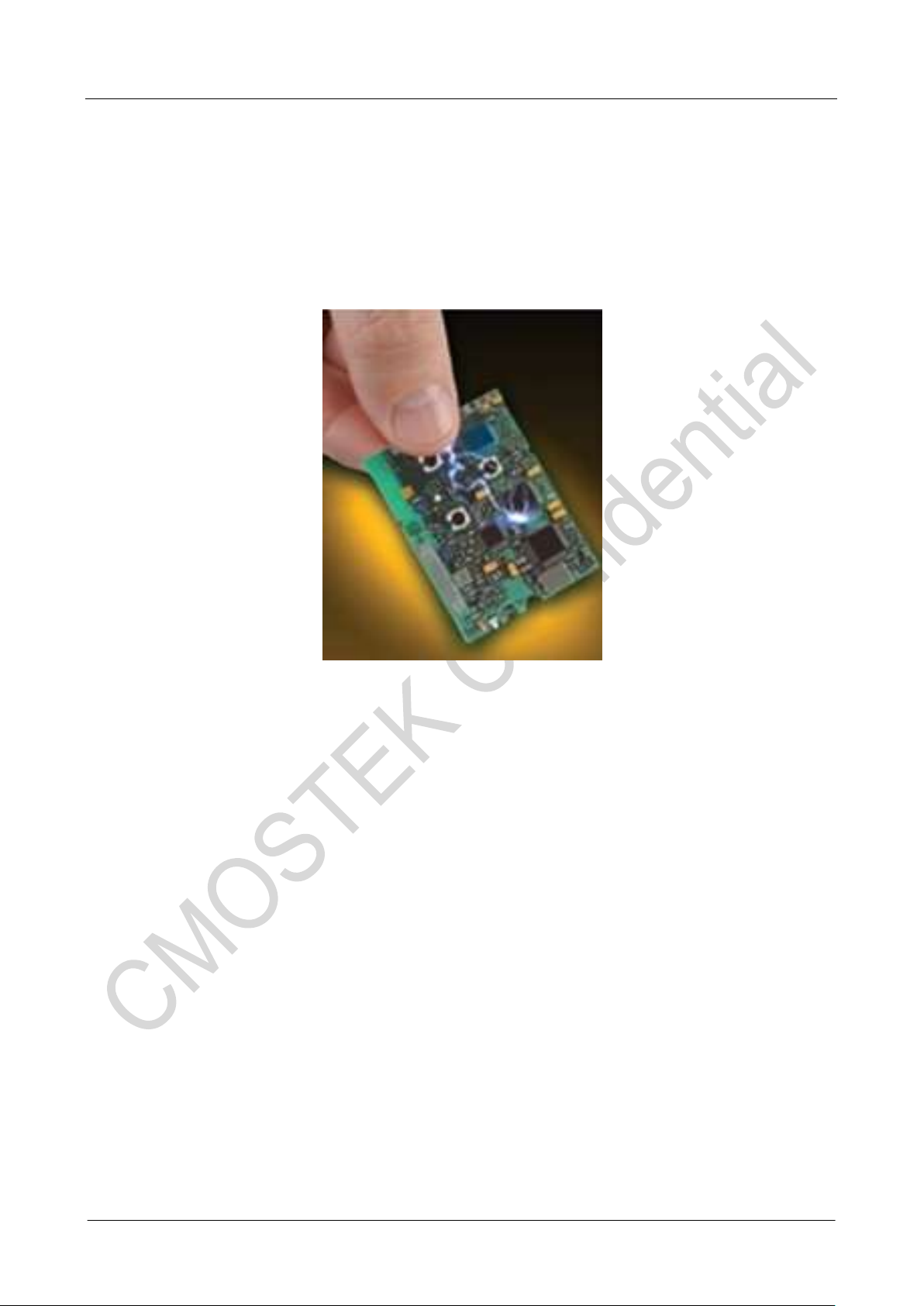
1 ESD Causes and Harms
Human Body Activity
Humidity 10-20%(V)
Humidity 65-90%(V)
Walking on chemical fiber floor cover
35,000
1,500
Taking a TEFLON wafer holder
30,000
1,200
Walking on chemical fiber floor
12,000
250
Working while sitting on a chair
6,000
100
Flipping a plastic sealed instruction book
7,000
600
Picking up a polyethylene bag
20,000
1,000
Sitting on a polyester foam pad
18,000
1,500
Electrostatic Voltage(V)
Human Body Response
1,000
Human body does not feel
2,000
Outside of fingers can feel
2,500
The discharging part can feel slight sharp-pain.
3,000
Can feel slight and moderate sharp-pain.
4,000
Fingers feel slight pain and strong sharp-pain.
5,000
Palm and wrist feel strong electric-shock.
6,000
Fingers feel very severe pain and the back of wrist feels strong electric-shock.
10,000
The whole wrist feels strong pain and the body feels current passing through.
12,000
Due to strong electric shock, the entire hand has a sense of heavy blow
Friction
Peeling
Induction
Causes of static electricity mainly includes friction, peeling and induction.
Figure 1. Main Causes of ESD Occurring
Under different humidity, the ESD cuased by various human body activities is different.
AN121
Table 2. Correlation between ESD Derived from Various Human Activity and Humidity
ESD can be generated even in a 99% humidity environment. The human body responses to ESD electrostatic voltages are as
follows (IEC 61000-4-2, human body model).
Table 3. Human Body Response to ESD Electrostatic Voltage
AN121
Rev 0.6 | 4/12
www.cmostek.com
2 ESD Transmission Route
For handheld devices, there exists potential difference between human bodies and handheld devices. As long as a potential
difference exists, there's a strong electric field established. Once the voltage exceeds the breakdown voltage between the air and
the insulating medium, an arc will be generated and it will keep until the conditions producing it disappear.
Figure 2. ESD of Handheld Devices
ESD can be introduced into handheld devices through 5 coupling paths as below.
1. The initial electric field energy can have capacitive couple with the trace networks which have a relatively large surface
area.
2. Charge/current is injected directly through the arc.
3. The current can cause voltage pulses (V = L × dI / dt) on the conductors such as power, ground and signal traces. The
current pulses will enter each common element connected in these networks.
4. The arc will produce a strong magnetic field with a frequency range of 1 MHz to 500 MHz and is inductively coupled to each
adjacent trace loop.
5. The electromagnetic field radiated by the arc will be coupled to long signal traces acting as receiving antennas.
ESD will catch the weak points of handheld devices through a variety of coupling paths. To avoid interference and damage from
ESD events, users should isolate these coupling paths or strengthen the anti-ESD capability accordingly.
 Loading...