

Page 1
Global LCD Panel Exchange Center
TFT LCD Approval Specification
MODEL NO.: V562D1–P01
Customer: _________________________________
www.panelook.com
Issue Date:Jun.18.2009
Model No.: V562D1-P01
Approval
Approved by:_______________________________
Note
TV Head Division
Approved By
LY Chen
QA Dept. Product Development Div.
Reviewed By
Hsin-nan Chen WT Lin
LCD TV Marketing and Product Management Div.
Prepared By
CY Chang Michell Tsung
1
One step solution for LCD / PDP / OLED panel application: Datasheet, inventory and accessory!
Version 2.0
www.panelook.com
Page 2

Global LCD Panel Exchange Center
www.panelook.com
Issue Date:Jun.18.2009
Model No.: V562D1-P01
Approval
CONTENTS
REVISION HISTORY......................................................................................................................................................... 4
1.
GENERAL DESCRIPTION ................................................................................................................................... 5
1.1.
OVERVIEW .................................................................................................................................................. 5
1.2.
FEATURES .................................................................................................................................................. 5
1.3.
APPLICATION ............................................................................................................................................. 5
1.4.
GENERAL SPECIFICATIONS ..................................................................................................................... 5
1.5.
MECHANICAL SPECIFICATIONS............................................................................................................... 6
2.
ABSOLUTE MAXIMUM RATINGS ....................................................................................................................... 7
2.1.
ABSOLUTE RATINGS OF ENVIRONMENT (BASE ON CMO MODULE V562D1-L04) ............................ 7
2.2.
PACKAGE STORAGE ................................................................................................................................. 8
2.3.
RATINGS OF IMAGE STICKING ................................................................................................................ 8
3.
ELECTRICAL MAXIMUM RATINGS .................................................................................................................... 9
3.1.
TFT LCD MODULE ...................................................................................................................................... 9
4.
5.
6.
7.
ELECTRICAL CHARACTERISTICS ................................................................................................................... 10
4.1.
TFT LCD MODULE .................................................................................................................................... 10
BLOCK DIAGRAM .............................................................................................................................................. 12
5.1.
TFT LCD MODULE .................................................................................................................................... 12
LCD INPUT TERMINAL PIN ASSIGNMENT ...................................................................................................... 13
6.1.
TFT LCD MODULE L.V.D.S. INPUT .......................................................................................................... 13
6.2.
TFT LCD MODULE POWER INPUT ......................................................................................................... 15
6.3.
BLOCK DIAGRAM OF IMAGE SIGNAL .................................................................................................... 16
6.4.
BLOCK DIAGRAM OF L.V.D.S. ................................................................................................................. 17
6.5.
L.V.D.S. INTERFACE ................................................................................................................................. 19
6.6.
COLOR DATA INPUT ASSIGNMENT ........................................................................................................ 20
TIMING REQUIREMENTS OF IMAGE SIGNAL ................................................................................................ 21
7.1.
INPUT SIGNAL TIMING SPECIFICATIONS .............................................................................................. 21
7.2.
POWER ON/OFF SEQUENCE ................................................................................................................. 23
8.
OPTICAL CHARACTERISTICS ......................................................................................................................... 24
2
One step solution for LCD / PDP / OLED panel application: Datasheet, inventory and accessory!
Version 2.0
www.panelook.com
Page 3
Global LCD Panel Exchange Center
8.1.
TEST CONDITIONS .................................................................................................................................. 24
8.2.
OPTICAL SPECIFICATIONS ..................................................................................................................... 24
9.
PRECAUTIONS .................................................................................................................................................. 29
9.1.
ASSEMBLY AND HANDLING PRECAUTIONS......................................................................................... 29
9.2.
SAFETY PRECAUTIO NS .......................................................................................................................... 29
9.3.
SAFETY STANDARDS .............................................................................................................................. 29
10.
DEFINITION OF LABELS ................................................................................................................................... 30
www.panelook.com
Issue Date:Jun.18.2009
Model No.: V562D1-P01
Approval
10.1.OPEN CELL LABEL ................................................................................................................................... 30
10.2.CARTON LABEL ........................................................................................................................................ 30
11.
PACKAGING ....................................................................................................................................................... 31
11.1.PACKING SPECIFICATIONS .................................................................................................................... 31
11.2.PACKING METHOD .................................................................................................................................. 31
12.
MECHANICAL CHARACTERISTIC .................................................................................................................... 33
3
One step solution for LCD / PDP / OLED panel application: Datasheet, inventory and accessory!
Version 2.0
www.panelook.com
Page 4
Global LCD Panel Exchange Center
REVISION HISTORY
Version Date Page(New) Section Description
Ver 2.0 Jun. 18,’09 All All Approval Specification is first issued.
www.panelook.com
Issue Date:Jun.18.2009
Model No.: V562D1-P01
Approval
4
One step solution for LCD / PDP / OLED panel application: Datasheet, inventory and accessory!
Version 2.0
www.panelook.com
Page 5
Global LCD Panel Exchange Center
1. GENERAL DESCRIPTION
1.1. OVERVIEW
V562D1-P01 is a 56” Thin-Film-Transistor Liquid-Crystal Display (TFT-LCD) cell with driver ICs and 8ch-LVDS
interface. This module supports 3840 x 2160 Quad Full High Definition (QFHD) TV format and can display 1G
colors (10-bit/color). The backlight unit is not built-in.
1.2. FEATURES
Ultra Wide Viewing Angle (176(H)/ 176(V) for CR>30)
Ultra Fast Response Time (Gray to gray average 6.5 ms)
Contrasty Image (Gamma 2.5)
QFHD (3840 x 2160 pixels) Resolution
8ch-LVDS (Low Voltage Differential Signaling) Interface
RoHS Compliance
www.panelook.com
Issue Date:Jun.18.2009
Model No.: V562D1-P01
Approval
1.3. APPLICATION
Luxurious Living Room TVs
Public Display
Home Theater
Satellite Communication
Medical Analyses/ Instruction
Security and Monitoring
Industrial Design
3D Display
Digital Museum
Multi-Media Display
1.4. GENERAL SPECIFICATIONS
CHARACTERISTICS ITEMS SPECIFICATIONS
Screen Diagonal [in] 56.2
Pixels [lines] 3840 × 2160
Active Area [mm] 1244.16 (H) x 699.84 (V) (56.2” diagonal)
Sub-Pixel Pitch [mm] 0.108 (H) x 0.324 (V)
Pixel Arrangement RGB vertical stripe
Weight [g] 3500
Physical Size [mm] 1269.0(W) x 724.7(H) x 1.82(D) Typ
Display Mode Transmissive mode / Normally black
Contrast Ratio 1500:1 Typ.
Glass thickness (Array / CF) [mm] 0.7 / 0.7
Viewing Angle (CR>30) +88/-88(H),+88/-88(V) Typ.
Color Chromaticity R=0.663, 0.325
(Typical value measured at CMO’s module)
(Typical value measured at CMO’s module)
G=0.266, 0.607
5
One step solution for LCD / PDP / OLED panel application: Datasheet, inventory and accessory!
Version 2.0
www.panelook.com
Page 6
Global LCD Panel Exchange Center
Cell Transparency [%] 3.1%Typ.
Polarizer Surface Treatment Anti-Glare coating (Haze 25%).
1.5. MECHANICAL SPECIFICATIONS
Item Min. Typ. Max. Unit Note
Weight 3000 3500 4000 g -
I/F connector mounting position
Note (1) Please refer to the attached drawings for more information of front and back outline dimensions.
www.panelook.com
B=0.141, 0.066
W=0.326, 0.355
(Typical value measured at CMO’s module)
(Typical value measured at CMO’s module)
Hardness 3H.
The mounting inclination of the connector makes the
screen center within ± 0.5mm as the horizontal.
Issue Date:Jun.18.2009
Model No.: V562D1-P01
Approval
(2)
Note (2) Connector mounting position
+/- 0.5mm
6
One step solution for LCD / PDP / OLED panel application: Datasheet, inventory and accessory!
Version 2.0
www.panelook.com
Page 7
Global LCD Panel Exchange Center
www.panelook.com
2. ABSOLUTE MAXIMUM RATINGS
2.1. ABSOLUTE RATINGS OF ENVIRONMENT (BASE ON CMO MODULE V562D1-L04)
Item Symbol
Storage Temperature T
Operating Ambient Temperature T
Shock (Non-Operating) S
Vibration (Non-Operating) V
Note (1) Temperature and relative humidity range is shown in the figure below.
(a) 90 %RH Max. (Ta Љ 40 ºC).
(b) Wet-bulb temperature should be 39 ºC Max. (Ta > 40 ºC).
(c) No condensation.
Note (2) The maximum operating temperature is based on the test condition that the surface temperature of
ST
OP
X, Y axis - 30 G (3), (5)
NOP
Z axis - 30 G (3), (5)
NOP
Min. Max.
Value
-20 +55 ºC (1)
0 45 ºC (1), (2)
- 1.0 G (4), (5)
Issue Date:Jun.18.2009
Model No.: V562D1-P01
Approval
Unit Note
display area is less than or equal to 65 ºC with LCD module alone in a temperature controlled chamber.
Thermal management should be considered in your product design to prevent the surface temperature
of display area from being over 65 ºC. The range of operating temperature may degrade in case of
improper thermal management in your product design.
Note (3) 11 ms, half sine wave, 1 time for ± X, ± Y, and ± Z.
Note (4) 10 ~ 200 Hz, 10 min, 1 time each X, Y, Z.
Note (5) At testing Vibration and Shock, the fixture in holding the module has to be hard and rigid enough so that
the module would not be twisted or bent by the fixture. The module would not be twisted or bent by the
fixture.
7
One step solution for LCD / PDP / OLED panel application: Datasheet, inventory and accessory!
Version 2.0
www.panelook.com
Page 8
Global LCD Panel Exchange Center
2.2. PACKAGE STORAGE
Storage condition: With shipping package.
Storage temperature rang: 25±5
Storage humidity range: 50±10%RH
Shelf life: a month
2.3. RATINGS OF IMAGE STICKING
Item Symbol Value Unit Note
Room Temperature Image Sticking RT IS Invisibility 6% ND (%) (1)(3)
High Temperature Image Sticking HT IS Invisibility 6% ND (%) (2)(3)
Note (1) Room temperature image sticking test is at 253 oC environment and fix the pattern A (checker pattern)
www.panelook.com
Issue Date:Jun.18.2009
Model No.: V562D1-P01
Approval
o
C
for 12 hours.
o
Note (2) High temperature image sticking test is at 503
Note (3) Inspection condition is at pattern B (512grade) after 5 mins from pattern A.
A. Pattern A (checker pattern) B. Pattern B (512grade)
C environment and fix the pattern A for 12 hours.
8
One step solution for LCD / PDP / OLED panel application: Datasheet, inventory and accessory!
Version 2.0
www.panelook.com
Page 9
Global LCD Panel Exchange Center
3. ELECTRICAL MAXIMUM RATINGS
3.1. TFT LCD MODULE
www.panelook.com
Issue Date:Jun.18.2009
Model No.: V562D1-P01
Approval
Item Symbol
V
-0.3 20 V
Power Supply Voltage
Logic Input Voltage VIN -0.3 3.6 V
Note (1) Permanent damage to the device may occur if maximum values are exceeded. Function operation
should be restricted to the conditions described under normal operating conditions.
CC1
V
-0.3 6 V
CC2
Value
Min. Max.
Unit Note
(1)
9
One step solution for LCD / PDP / OLED panel application: Datasheet, inventory and accessory!
Version 2.0
www.panelook.com
Page 10
Global LCD Panel Exchange Center
4. ELECTRICAL CHARACTERISTICS
4.1. TFT LCD MODULE
Parameter Symbol
Power Supply Voltage
Power Supply Ripple Voltage
Rush Current
White
Black - 1.8 - A
Power Supply Current
Vertical Stripe - 3.5 - A
White
Black - 4.9 - A
Vertical Stripe - 5.4 5.9 A
Differential Input High
Threshold Voltage
LVDS
Interface
Differential Input Low
Threshold Voltage
Common Input Voltage V
Terminating Resistor RT 100 ohm
CMOS
Interface
Input High Threshold Voltage V
Input Low Threshold Voltage VIL 0 - 0.7 V
Note (1) The module should be always operated within the above ranges.
www.panelook.com
Issue Date:Jun.18.2009
Model No.: V562D1-P01
Value
Min. Typ. Max.
17.1 18 18.9 V
V
CC1
V
4.5 5 5.5 V
CC2
- - 400 mV
V
RP1
V
200 mV
RP2
- - 8 A
I
RUSH1
I
- - 7.5 A
RUSH2
- 4.2 4.7 A
I
CC1
- 5 - A
I
CC2
V
- - +100 mV
LVTH
V
-100 - mV
LVTL
1.125 1.25 1.375 V
LVC
2.7 - 3.3 V
IH
Unit Note
Approval
(1)
(2)
(3)
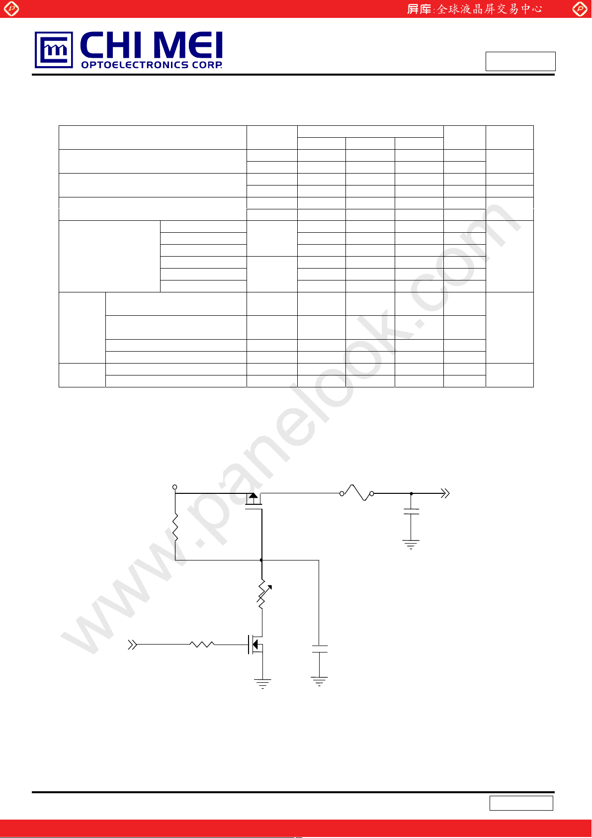
Note (2) Measurement conditions:
+5V or +18V
+5.0V or
R1
1K
(Low to High)
(Control Signal)
SW
R2
1K
Q1
Si4485DY
47K
Q2
2N7002
VR1
C1
0.01uF
FUSE
C3
1uF
Vcc1 or
(LCD Module Input)
10
One step solution for LCD / PDP / OLED panel application: Datasheet, inventory and accessory!
Version 2.0
www.panelook.com
Page 11
Global LCD Panel Exchange Center
GND
Note (3) The specified power supply current is under the conditions at Vcc1 = 18 V, Vcc2 = 5 V, Ta = 25 ± 2 ºC,
f
= 60 Hz, whereas a power dissipation check pattern below is displayed.
v
www.panelook.com
Issue Date:Jun.18.2009
Model No.: V562D1-P01
Approval
Vcc rising time is at least 470μs
0.9Vcc
0.1Vcc
470μs
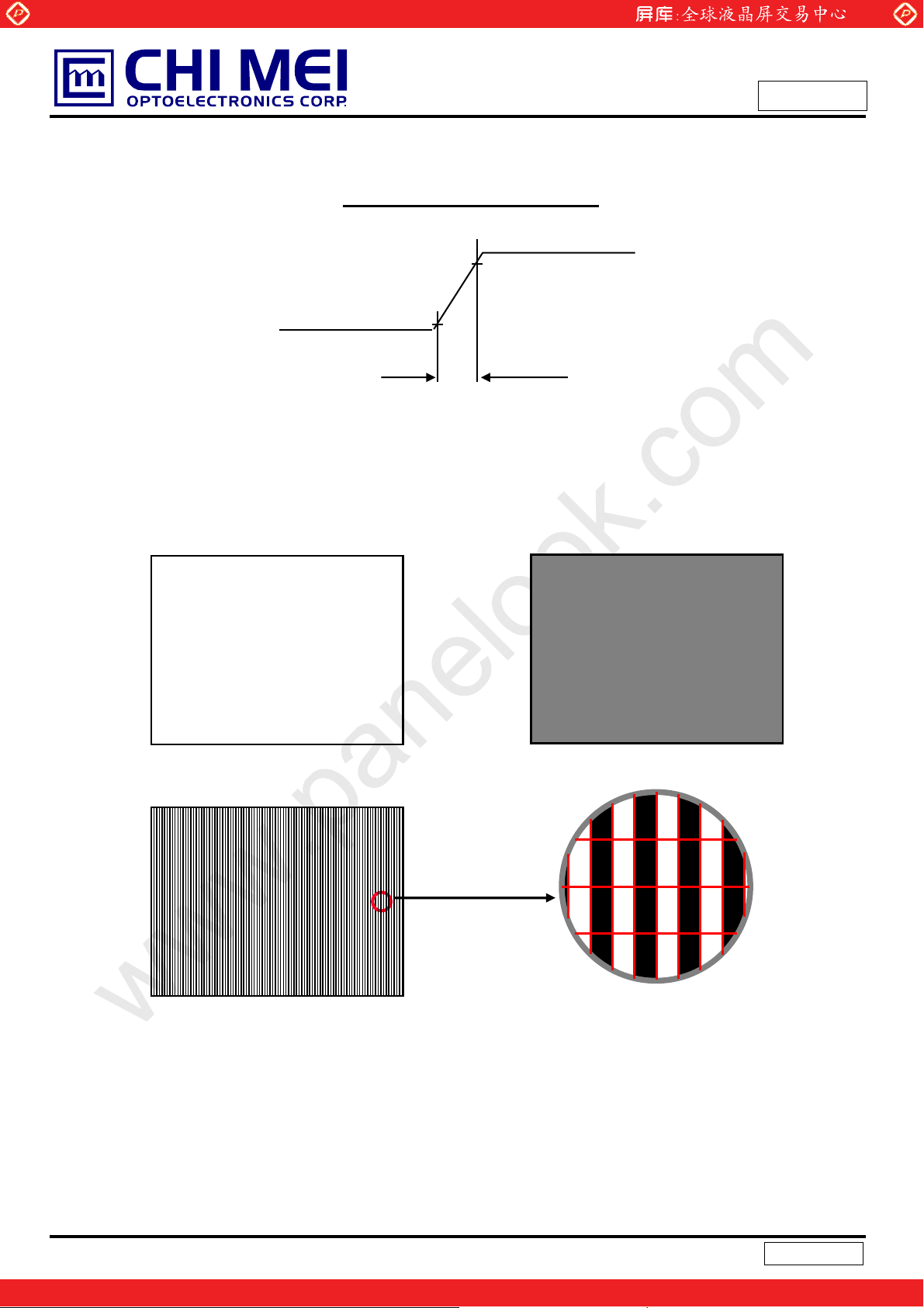
a. White Pattern
c. Vertical Stripe Pattern
b. Black Pattern
Active Area Active Area
G
R
G
B
R
G
B
R
G
R R
B
B
B
B
B
G
R
R
B
G
R
R
B
G
R
B
G
Active Area
11
One step solution for LCD / PDP / OLED panel application: Datasheet, inventory and accessory!
Version 2.0
www.panelook.com
Page 12
Global LCD Panel Exchange Center
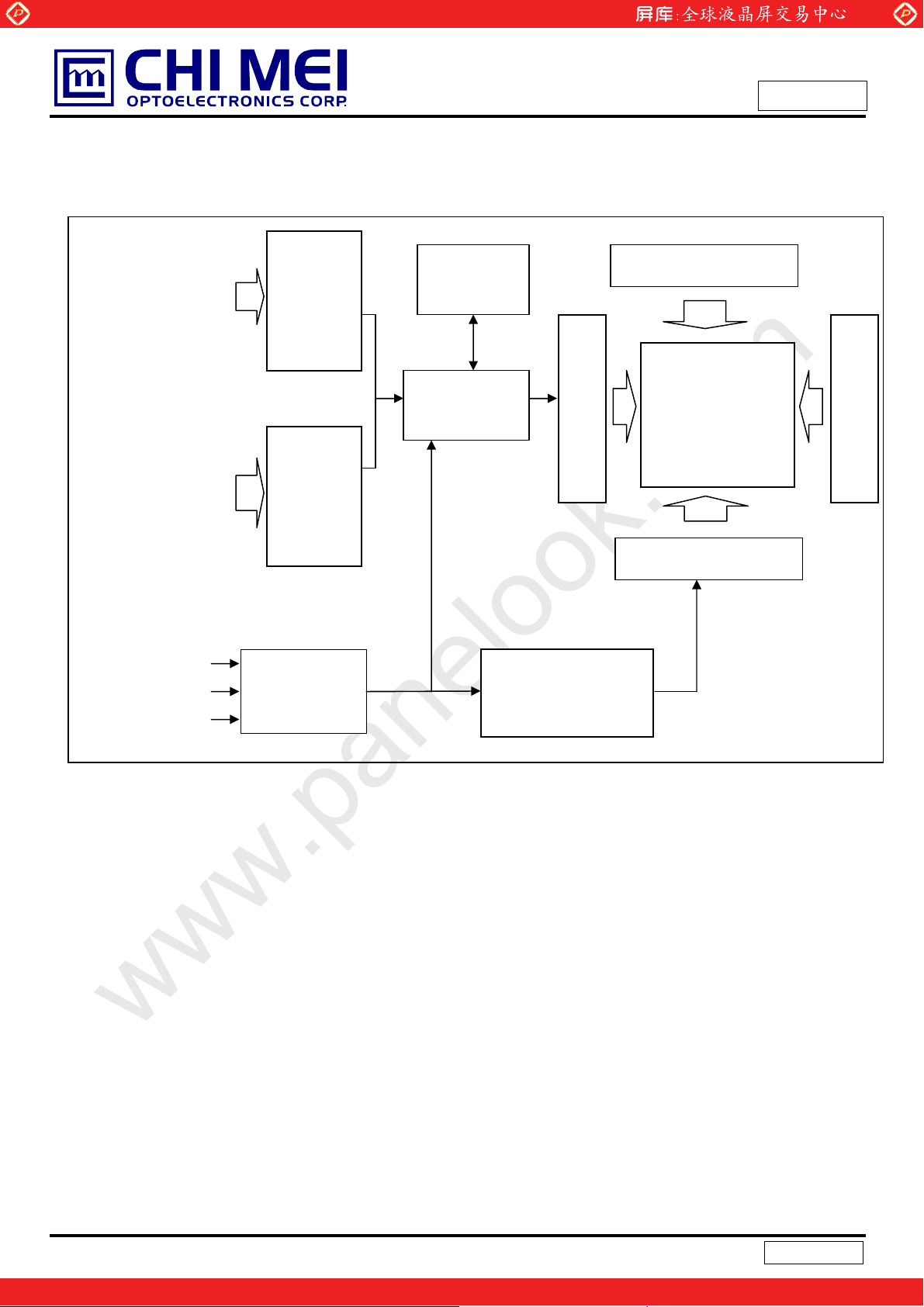
5. BLOCK DIAGRAM
5.1. TFT LCD MODULE
www.panelook.com
Issue Date:Jun.18.2009
Model No.: V562D1-P01
Approval
2B_Odd_Data0(+/-)
2B_Odd_Data1(+/-)
2B_Odd_Data2(+/-)
2B_Odd_Data3(+/-)
2B_Odd_Data4(+/-)
2B_Odd_Clock(+/-)
2B_Even_Data0(+/-)
2B_Even_Data1(+/-)
2B_Even_Data2(+/-)
2B_Even_Data3(+/-)
2B_Even_Data4(+/-)
2B_Even_Clock(+/-)
1B_Odd_Data0(+/-)
1B_Odd_Data1(+/-)
1B_Odd_Data2(+/-)
1B_Odd_Data3(+/-)
1B_Odd_Data4(+/-)
1B_Odd_Clock(+/-)
1B_Even_Data0(+/-)
1B_Even_Data1(+/-)
1B_Even_Data2(+/-)
1B_Even_Data3(+/-)
1B_Even_Data4(+/-)
1B_Even_Clock(+/-)
2A_Odd_Data0(+/-)
2A_Odd_Data1(+/-)
2A_Odd_Data2(+/-)
2A_Odd_Data3(+/-)
2A_Odd_Data4(+/-)
2A_Odd_Clock(+/-)
2A_Even_Data0(+/-)
2A_Even_Data1(+/-)
2A_Even_Data2(+/-)
2A_Even_Data3(+/-)
2A_Even_Data4(+/-)
2A_Even_Clock(+/-)
1A_Odd_Data0(+/-)
1A_Odd_Data1(+/-)
1A_Odd_Data2(+/-)
1A_Odd_Data3(+/-)
1A_Odd_Data4(+/-)
1A_Odd_Clock(+/-)
1A_Even_Data0(+/-)
1A_Even_Data1(+/-)
1A_Even_Data2(+/-)
1A_Even_Data3(+/-)
1A_Even_Data4(+/-)
1A_Even_Clock(+/-)
Vcc1
Vcc2
GND
B-F,FI-RE51S-HF,
CONNECTOR
JAE Taiwan.
INPUT
CN6
CN7
B-F,FI-RE51S-HF,
CONNECTOR
JAE Taiwan.
INPUT
CN3.
POWER
CONNECTOR
(S20B-PHDS
S-B(LF)(SN))
FRAME
BUFFER
TIMING
CONTROLLER
DC/DC CONVERTER
SCAN DRIVER
& REFERENCE
VOLTAGE
GENERATOR
DATA DRIVER (RSDS)
SCAN DRIVER
TFT LCD PANEL
(3840x3x2160)
DATA DRIVER (RSDS)
12
One step solution for LCD / PDP / OLED panel application: Datasheet, inventory and accessory!
Version 2.0
www.panelook.com
Page 13

Global LCD Panel Exchange Center
6. LCD INPUT TERMINAL PIN ASSIGNMENT
6.1. TFT LCD MODULE L.V.D.S. INPUT
CN6 Connector Pin Assignment
Pin No. Name Description Note
1 GND Ground.
2 2B_FRX0- Negative transmission data of First pixel 0.
3 2B_FRX0+ Positive transmission data of First pixel 0.
4 2B_FRX1- Negative transmission data of First pixel 1.
5 2B_FRX1+ Positive transmission data of First pixel 1.
6 2B_FRX2- Negative transmission data of First pixel 2.
7 2B_FRX2+ Positive transmission data of First pixel 2.
8 2B_ FCLK- Negative of First clock.
9 2B_ FCLK+ Positive of First clock.
10 2B_FRX3- Negative transmission data of First pixel 3.
11 2B_FRX3+ Positive transmission data of First pixel 3.
12 2B_FRX4- Negative transmission data of First pixel 4.
13 2B_FRX4+ Positive transmission data of First pixel 4.
14 2B_SRX0- Negative transmission data of Second pixel 0.
15 2B_SRX0+ Positive transmission data of Second pixel 0.
16 2B_SRX1- Negative transmission data of Second pixel 1.
17 2B_SRX1+ Positive transmission data of Second pixel 1.
18 2B_SRX2- Negative transmission data of Second pixel 2.
19 2B_SRX2+ Positive transmission data of Second pixel 2.
20 2B_ SCLK- Negative of Second clock.
21 2B_ SCLK+ Positive of Second clock.
22 2B_SRX3- Negative transmission data of Second pixel 3.
23 2B_SRX3+ Positive transmission data of Second pixel 3.
24 2B_SRX4- Negative transmission data of Second pixel 4.
25 2B_SRX4+ Positive transmission data of Second pixel 4.
26 GND Ground.
27 2A_FRX0- Negative transmission data of First pixel 0.
28 2A_FRX0+ Positive transmission data of First pixel 0.
29 2A_FRX1- Negative transmission data of First pixel 1.
30 2A_FRX1+ Positive transmission data of First pixel 1.
31 2A_FRX2- Negative transmission data of First pixel 2.
32 2A_FRX2+ Positive transmission data of First pixel 2.
33 2A_ FCLK- Negative of First clock.
34 2A_ FCLK+ Positive of First clock.
35 2A_FRX3- Negative transmission data of First pixel 3.
36 2A_FRX3+ Positive transmission data of First pixel 3.
37 2A_FRX4- Negative transmission data of First pixel 4.
38 2A_FRX4+ Positive transmission data of First pixel 4.
39 2A_SRX0- Negative transmission data of Second pixel 0.
40 2A_SRX0+ Positive transmission data of Second pixel 0.
41 2A_SRX1- Negative transmission data of Second pixel 1.
42 2A_SRX1+ Positive transmission data of Second pixel 1.
43 2A_SRX2- Negative transmission data of Second pixel 2.
44 2A_SRX2+ Positive transmission data of Second pixel 2.
45 2A_ SCLK- Negative of Second clock.
46 2A_ SCLK+ Positive of Second clock.
47 2A_SRX3- Negative transmission data of Second pixel 3.
48 2A_SRX3+ Positive transmission data of Second pixel 3.
49 2A_SRX4- Negative transmission data of Second pixel 4.
www.panelook.com
Issue Date:Jun.18.2009
Model No.: V562D1-P01
Approval
13
One step solution for LCD / PDP / OLED panel application: Datasheet, inventory and accessory!
Version 2.0
www.panelook.com
Page 14

Global LCD Panel Exchange Center
50 2A_SRX4+ Positive transmission data of Second pixel 4.
51 GND Ground.
CN7 Connector Pin Assignment
Pin No. Name Description Note
1 GND Ground.
2 1B_FRX0- Negative transmission data of First pixel 0.
3 1B_FRX0+ Positive transmission data of First pixel 0.
4 1B_FRX1- Negative transmission data of First pixel 1.
5 1B_FRX1+ Positive transmission data of First pixel 1.
6 1B_FRX2- Negative transmission data of First pixel 2.
7 1B_FRX2+ Positive transmission data of First pixel 2.
8 1B_ FCLK- Negative of First clock.
9 1B_ FCLK+ Positive of First clock.
10 1B_FRX3- Negative transmission data of First pixel 3.
11 1B_FRX3+ Positive transmission data of First pixel 3.
12 1B_FRX4- Negative transmission data of First pixel 4.
13 1B_FRX4+ Positive transmission data of First pixel 4.
14 1B_SRX0- Negative transmission data of Second pixel 0.
15 1B_SRX0+ Positive transmission data of Second pixel 0.
16 1B_SRX1- Negative transmission data of Second pixel 1.
17 1B_SRX1+ Positive transmission data of Second pixel 1.
18 1B_SRX2- Negative transmission data of Second pixel 2.
19 1B_SRX2+ Positive transmission data of Second pixel 2.
20 1B_ SCLK- Negative of Second clock.
21 1B_ SCLK+ Positive of Second clock.
22 1B_SRX3- Negative transmission data of Second pixel 3.
23 1B_SRX3+ Positive transmission data of Second pixel 3.
24 1B_SRX4- Negative transmission data of Second pixel 4.
25 1B_SRX4+ Positive transmission data of Second pixel 4.
26 GND Ground.
27 1A_FRX0- Negative transmission data of First pixel 0.
28 1A_FRX0+ Positive transmission data of First pixel 0.
29 1A_FRX1- Negative transmission data of First pixel 1.
30 1A_FRX1+ Positive transmission data of First pixel 1.
31 1A_FRX2- Negative transmission data of First pixel 2.
32 1A_FRX2+ Positive transmission data of First pixel 2.
33 1A_ FCLK- Negative of First clock.
34 1A_ FCLK+ Positive of First clock.
35 1A_FRX3- Negative transmission data of First pixel 3.
36 1A_FRX3+ Positive transmission data of First pixel 3.
37 1A_FRX4- Negative transmission data of First pixel 4.
38 1A_FRX4+ Positive transmission data of First pixel 4.
39 1A_SRX0- Negative transmission data of Second pixel 0.
40 1A_SRX0+ Positive transmission data of Second pixel 0.
41 1A_SRX1- Negative transmission data of Second pixel 1.
42 1A_SRX1+ Positive transmission data of Second pixel 1.
43 1A_SRX2- Negative transmission data of Second pixel 2.
44 1A_SRX2+ Positive transmission data of Second pixel 2.
45 1A_ SCLK- Negative of Second clock.
46 1A_ SCLK+ Positive of Second clock.
47 1A_SRX3- Negative transmission data of Second pixel 3.
48 1A_SRX3+ Positive transmission data of Second pixel 3.
www.panelook.com
Issue Date:Jun.18.2009
Model No.: V562D1-P01
Approval
14
One step solution for LCD / PDP / OLED panel application: Datasheet, inventory and accessory!
Version 2.0
www.panelook.com
Page 15

Global LCD Panel Exchange Center
49 1A_SRX4- Negative transmission data of Second pixel 4.
50 1A_SRX4+ Positive transmission data of Second pixel 4.
51 GND Ground.
Note (1) CN6&CN7 connector part no.: B-F,FI-RE51S-HF,JAE Taiwan.
6.2. TFT LCD MODULE POWER INPUT
CN3 Connector Pin Assignment
Pin No. Symbol Description Note
1 VIN +18.0V power supply
2 VIN +18.0V power supply
3 V5VC +5.0V power supply
4 V5VC +5.0V power supply
5 V5VC +5.0V power supply
6 NC Not connection
7 V5VC +5.0V power supply
8 NC Not connection
9 V5VC +5.0V power supply
10 NC Not connection
11 GND Ground
12 NC Not connection
13 GND Ground
14 NC Not connection
15 GND Ground
16 ODSEL Overdrive Lookup Table Selection (2)(3)
17 GND Ground
18 GND Ground
19 GND Ground
20 GND Ground
Note (1) CN3 connector part no.: S20B-PHDSS-B(LF)(SN), JST(ֲءᚘထጤ),ᐚຏጤ or equivalent.
www.panelook.com
Issue Date:Jun.18.2009
Model No.: V562D1-P01
Approval
Note (2) ODSEL (Overdrive Lookup Table Selection). The overdrive lookup table should be selected in
accordance to the frame rate to optimize image quality.
ODSEL Note
L Lookup table was optimized for 60Hz frame rate.
H Lookup table was optimized for 50Hz frame rate.
Note (3) “L” and “H” operation in (3) could follow “CMOS Interface” in Section 4.1
15
One step solution for LCD / PDP / OLED panel application: Datasheet, inventory and accessory!
Version 2.0
www.panelook.com
Page 16

Global LCD Panel Exchange Center
6.3. BLOCK DIAGRAM OF IMAGE SIGNAL
The video picture (3840x2160) should be divided into four parts: the left up side (1920x1080), the left down side
(1920x1080), the right up side (1920x1080) and the right down side (1920x1080). Signals of these four parts
should be delivered into the module individually through each 2-channel LVDS interface. But it must be
“synchronous” mutually between signals from these four 2-channel LVDS interfaces. And the protocol is specified
in the LVDS interface specification.
www.panelook.com
Issue Date:Jun.18.2009
Model No.: V562D1-P01
Approval
Note (1) It must be “synchronous” mutually between signals from CN6(2A/2B) and CN7(1A/1B).
Note (2) It exists 1/3 frame buffer (i.e. buffer =1/3 x 1920 x1080 pixels) between CN6(2A/2B) and CN7(1A/1B)
CN3
CC Board
CN6
Note (1) It must be “synchronous” mutually between signals from CN6(2A) and CN6(2B).
Note (2) It must be “synchronous” mutually between signals from CN7(2A) and CN7(2B).
Note (3) It exists 1/3 frame buffer (i.e. buffer =1/3 x 1920 x1080 pixels) between CN6 and CN7.
CN7
16
One step solution for LCD / PDP / OLED panel application: Datasheet, inventory and accessory!
Version 2.0
www.panelook.com
Page 17

Global LCD Panel Exchange Center
6.4. BLOCK DIAGRAM OF L.V.D.S.
FRX0+
www.panelook.com
Issue Date:Jun.18.2009
Model No.: V562D1-P01
Approval
FRX0-
FRX1+
FRX1-
FRX2+
FRX2-
FRX3+
FRX3-
FRX4+
FRX4-
FCLK+
FCLK-
SRX0+
Rx-OUT
FR0-FR9
FG0-FG9
FB0-FB9
DE
SR0-SR9
SG0-SG9
SB0-SB9
DCLK
PLL
Timing Controller
SRX0-
SRX1+
SRX1-
SRX2+
SRX2-
SRX3+
SRX3-
SRX4+
SRX4-
SCLK+
SCLK-
LVDS Input
PLL
LVDS Receiver
17
One step solution for LCD / PDP / OLED panel application: Datasheet, inventory and accessory!
Version 2.0
www.panelook.com
Page 18

Global LCD Panel Exchange Center
FR0~FR9 : First pixel R data
FG0~FG9 : First pixel G data
FB0~FB9 : First pixel B data
SR0~SR9 : Second pixel R data
SG0~SG9 : Second pixel G data
SB0~SB9 : Second pixel B data
DE : Data enable signal
DCLK : Data clock signal
Note (1) The driving system must have the transmitter to drive the module.
Note (2) LVDS cable impedance shall be 50 ohms per signal line or about 100 ohms per twist-pair line when it is
used differentially.
www.panelook.com
Issue Date:Jun.18.2009
Model No.: V562D1-P01
Approval
Note (3) Two pixel data are sent into the module for every clock cycle.
18
One step solution for LCD / PDP / OLED panel application: Datasheet, inventory and accessory!
Version 2.0
www.panelook.com
Page 19

Global LCD Panel Exchange Center
6.5. L.V.D.S. INTERFACE
www.panelook.com
Issue Date:Jun.18.2009
Model No.: V562D1-P01
Approval
R0~R9 : Pixel R Data (9; MSB, 0; LSB)
G0~G9 : Pixel G Data (9; MSB, 0; LSB)
B0~B9 : Pixel B Data (9; MSB, 0; LSB)
DE : Data enable signal
RCLK : Data clock signal
Note (1) RSVD (reserved)pins on the transmitter shall be “H” or “L”.
19
One step solution for LCD / PDP / OLED panel application: Datasheet, inventory and accessory!
Version 2.0
www.panelook.com
Page 20

Global LCD Panel Exchange Center
6.6. COLOR DATA INPUT ASSIGNMENT
The brightness of each primary color (red, green and blue) is based on the 10-bit gray scale data input for
the color. The higher the binary input the brighter the color. The table below provides the assignment of color
versus data input.
www.panelook.com
Issue Date:Jun.18.2009
Model No.: V562D1-P01
Approval
Basic
Colors
Gray
Scale
Of
Red
Gray
Scale
Of
Green
Gray
Scale
Of
Blue
Color
Black
Red
Green
Blue
Cyan
Magenta
Yellow
White
Red (0) / Dark
Red (1)
Red (2)
:
:
Red (1021)
Red (1022)
Red (1023)
Green (0) / Dark
Green (1)
Green (2)
:
:
Green (1021)
Green (1022)
Green (1023)
Blue (0) / Dark
Blue (1)
Blue (2)
:
:
Blue (1021)
Blue (1022)
Blue (1023)
0
0
1
0
1
0
1
1
0
0
0
:
:
0
0
0
0
0
0
:
:
1
1
1
0
0
0
:
:
0
0
0
Data Signal
0
0
0
0
1
1
0
0
1
1
0
0
1
1
1
1
0
0
0
0
0
0
:
:
:
:
0
0
0
0
0
0
0
0
0
0
0
0
:
:
:
:
1
1
1
1
1
1
0
0
0
0
0
0
:
:
:
:
0
0
0
0
0
0
0
0
0
0
0
0
0
0
0
0
0
0
0
0
0
0
0
0
0
0
0
0
0
1
1
1
1
1
0
0
0
1
1
1
0
0
0
1
1
1
1
1
1
0
0
0
0
0
0
0
0
0
:
:
:
:
:
:
0
0
0
0
0
0
0
0
0
0
0
0
0
0
0
0
0
0
:
:
:
:
:
:
1
1
1
1
1
1
1
1
1
0
0
0
0
0
0
0
0
0
:
:
:
:
:
:
0
0
0
0
0
0
0
0
0
1
0
0
0
1
1
1
0
0
0
1
1
1
1
1
1
0
0
0
0
0
0
0
0
0
:
:
:
:
:
:
0
0
0
0
0
0
0
0
0
0
0
0
1
0
0
0
0
1
:
:
:
:
:
:
0
1
1
1
0
1
1
1
1
0
0
0
0
0
0
0
0
0
:
:
:
:
:
:
0
0
0
0
0
0
0
0
0
0
0
0
0
1
1
1
1
1
1
1
1
1
0
0
0
1
1
1
0
0
0
0
0
0
0
0
0
:
:
:
;
:
:
0
0
0
0
0
0
0
0
0
0
0
0
0
0
0
0
0
0
:
:
:
:
:
:
0
0
0
0
0
0
0
0
0
0
0
0
0
0
0
0
0
0
:
:
:
:
:
:
1
1
1
1
1
1
1
1
1
0
0
0
0
0
1
1
1
1
1
1
1
1
1
0
0
0
1
1
1
0
0
0
0
0
0
0
0
0
:
:
:
:
:
:
0
0
0
0
0
0
0
0
0
0
0
0
0
0
0
0
0
0
:
:
:
:
:
:
0
0
0
0
0
0
0
0
0
0
0
0
0
0
0
0
0
0
:
:
:
:
:
:
1
1
1
1
1
1
1
1
1
0
0
0
0
0
0
0
1
1
1
1
1
1
1
1
1
0
0
0
1
1
1
0
0
0
0
0
0
0
0
0
:
:
:
:
:
:
0
0
0
0
0
0
0
0
0
0
0
0
0
0
0
0
0
0
:
:
:
:
:
:
0
0
0
0
0
0
0
0
0
0
0
0
0
0
0
0
0
1
:
:
:
:
:
:
1
1
0
1
1
1
1
1
1
R9 R8 R7 R6 R5 R4 R3 R2 R1 R0 G9 G8 G7 G6 G5 G4 G3 G2 G1 G0 B9 B8 B7 B6 B5 B4 B3 B2 B1 B0
0
0
1
1
0
0
0
0
0
0
1
1
1
1
1
1
0
0
0
0
0
0
1
1
1
1
1
1
0
0
0
0
0
0
:
:
:
:
0
0
0
0
0
0
0
0
0
0
0
0
:
:
:
:
0
0
0
0
0
0
Red Green Blue
0
0
0
0
0
0
0
0
1
1
1
1
1
0
0
0
0
0
0
0
0
0
1
1
1
1
1
1
1
1
1
0
0
0
0
0
0
0
0
0
:
:
:
:
:
:
1
1
1
1
1
1
1
1
1
0
0
0
0
0
0
0
0
0
:
:
:
:
:
:
0
0
0
0
0
0
0
0
0
0
0
0
0
0
0
0
0
0
:
:
:
:
:
:
0
0
0
0
0
0
0
0
0
1
0
0
0
0
0
0
0
0
0
1
1
1
1
1
1
1
1
1
0
0
0
0
0
0
0
0
0
:
:
:
:
:
:
1
1
1
1
1
1
1
1
1
0
0
0
0
0
0
0
0
0
:
:
:
:
:
:
0
0
0
0
0
0
0
0
0
0
0
0
0
0
0
0
0
0
:
:
:
:
:
:
0
0
0
0
0
0
0
0
0
0
1
1
0
0
0
1
0
0
0
0
0
1
1
1
0
1
1
1
1
1
1
0
0
0
0
1
0
1
0
0
:
:
:
:
:
:
0
1
0
1
0
0
1
1
0
0
0
0
0
0
0
0
0
0
:
:
:
:
:
:
0
0
1
0
0
1
0
0
1
0
0
0
0
0
0
0
0
0
:
:
:
:
:
:
0
0
0
0
0
0
0
0
0
0
0
0
1
1
1
0
1
0
0
0
:
:
0
0
0
0
0
0
:
:
0
0
0
0
1
0
:
:
1
0
1
Note (1) 0: Low Level Voltage, 1: High Level Voltage
20
One step solution for LCD / PDP / OLED panel application: Datasheet, inventory and accessory!
Version 2.0
www.panelook.com
Page 21

Global LCD Panel Exchange Center
www.panelook.com
7. TIMING REQUIREMENTS OF IMAGE SIGNAL
7.1. INPUT SIGNAL TIMING SPECIFICATIONS
The input signal timing specifications are shown as the following table and timing diagram.
Signal Item Symbol Min. Typ. Max. Unit Note
LVDS Receiver Clock
(1-CH LVDS)
LVDS Receiver Data
Vertical Active Display Term
(2-CH LVDS,1920X1080 Active Area)
Horizontal Active Display Term
(2-CH LVDS, 1920x1080 Active Area)
Note (1) Since this module is operated in DE only mode, Hsync and Vsync input signals should be set to
Frequency 1/Tc 60 74 75 MHZ (1)
Input cycle to
cycle jitter
Setup Time Tlvsu 600 - - ps
Hold Time Tlvhd 600 - - ps
Frame Rate
Total Tv 1115 1125 1139 Th Tv=Tvd+Tvb
Display Tvd - 1080 - Th
Blank Tvb 35 45 55 Th
Total Th 2190 2200 2300 Tc Th=Thd+Thb
Display Thd - 1920 - Tc
Blank Thb 270 280 380 Tc
Issue Date:Jun.18.2009
Model No.: V562D1-P01
Approval
Trcl - - 200 ps
5
47 50 53 Hz (2)
Fr
Fr6 57 60 60 Hz (3)
low logic level. Otherwise, this module would operate abnormally.
Note (2) (ODSEL) = (H). Please refer to Section 6.2 for detail information.
Note (3) (ODSEL) = (L). Please refer to Section 6.2 for detail information.
INPUT SIGNAL TIMING DIAGRAM
T
v
T
vd
DE
T
h
Д
DCLK
Д
T
c
T
T
hb
hd
T
vb
Д
Д
DE
DATA
Valid display data (960 DCLK)
21
One step solution for LCD / PDP / OLED panel application: Datasheet, inventory and accessory!
Version 2.0
www.panelook.com
Page 22

Global LCD Panel Exchange Center
RXCLK+/-
RXn+/-
www.panelook.com
Issue Date:Jun.18.2009
Model No.: V562D1-P01
Approval
LVDS RECEIVER TIMING DIAGRAM
Tc
Tlvsu
Tlvhd
1T
14
3T
14
5T
14
7T
14
9T
14
11T
14
13T
14
22
One step solution for LCD / PDP / OLED panel application: Datasheet, inventory and accessory!
Version 2.0
www.panelook.com
Page 23

Global LCD Panel Exchange Center
7.2. POWER ON/OFF SEQUENCE
To prevent a latch-up or DC operation of LCD module, the power on/off sequence should be followed as the
diagram below.
ˣ˸ʳ˦˿
ˣ˸ʳ˦˿
ˣ˸ʳ˦˿ˣ˸ʳ˦˿
˩˶˶˄ʿʳ˩˶˶˅
www.panelook.com
˃ˁˌ˩˶˶˄
Issue Date:Jun.18.2009
Model No.: V562D1-P01
Approval
˃ˁˌ˩˶˶˄
˃ˁˈЉ˧˄Љ˄˃ʻ˩˶˶˄ʼ
˃ˁˈЉ˧ˊЉ˄˃ʻ˩˶˶˅ʼ
˃Љ˧ˋЉˈ˃
˃Љ˧˅Љˈ˃
˃Љ˧ˆЉˈ˃
ˈ˃˃Љ˧ˇ
˦˼˺˴˿
˦˼˺˴˿
˦˼˺˴˿˦˼˺˴˿
˕˴˶˾˿˼˺˻ʳʻ˥˸˶˸˷˸˷ʼ
˄ˈ˃˃Љ˧ˈ
˄˃˃Љ˧ˉ
˃˩
˃˩
˃˩
˃ˁ˄˩˶˶˄
˧˄
˧˄
˧˄˧˄
˃ˁˌ˩˶˶˅
˃ˁ˄˩˶˶˅
˧ˋ
˧ˋ
˧ˋ˧ˋ
˧ˊ
˧ˊ
˧ˊ˧ˊ
˧˅
˧˅
˧˅˧˅
˃ˁˌ˩˶˶˅
˧ˆ
˧ˆ
˧ˆ˧ˆ
˩˔˟˜˗
ˣ˸ʳˢ ˣ˸ʳˢ˹˹
ˈ˃ʸ ˈ˃ʸ
˧ˈ
˧ˈ ˧ˉ
˧ˈ˧ˈ
ˣ˸ʳˢˡ˂ˢ˙˙ʳ˦˸˸˶˸
ˣ˸ʳˢˡ˂ˢ˙˙ʳ˦˸˸˶˸
ˣ˸ʳˢˡ˂ˢ˙˙ʳ˦˸˸˶˸ˣ˸ʳˢˡ˂ˢ˙˙ʳ˦˸˸˶˸
˧ˉ
˧ˉ˧ˉ
˃ˁ˄˩˶˶˄
˃ˁ˄˩˶˶˅
˧ˇ
˧ˇ
˧ˇ˧ˇ
Note (1) The supplied voltage of the external system for the module input should follow the definition of Vcc1,2.
Note (2) Apply the lamp voltage within the LCD operation range. When the backlight turns on before the LCD
operation or the LCD turns off before the backlight turns off, the display may momentarily become
abnormal screen.
Note (3) In case of Vcc1,2 is in off level, please keep the level of input signals on the low and avoid floating.
Note (4) T4 should be measured after the module being fully discharged between power off and on period.
Note (5) Interface signal shall not be kept at high impedance when the power is on.
23
One step solution for LCD / PDP / OLED panel application: Datasheet, inventory and accessory!
Version 2.0
www.panelook.com
Page 24

Global LCD Panel Exchange Center
x
Y
8. OPTICAL CHARACTERISTICS
8.1. TEST CONDITIONS
Item Symbol Value Unit
Ambient Temperature Ta
Ambient Humidity Ha
Supply Voltage V
Input Signal According to typical value in "3. ELECTRICAL CHARACTERISTICS"
Frame Rate F
8.2. OPTICAL SPECIFICATIONS
The relative measurement methods of optical characteristics are shown in 8.2. The following items should be
measured under the test conditions described in 8.1 and stable environment shown in Note (6).
Item Symbol Condition Min. Typ. Max. Unit Note
Contrast Ratio CR
Response Time Gray to gray 6.5 ms (5)
Transmittance T% 3.1 % (2),(10)
White Variation
Cross Talk CT 2 % (2),(7)
Red
Green
Color
Chromaticity
Blue
White
Horizontal
Viewing
Angle
Ver t ic a l
Note (1) Light source is the standard light source “C” which is defined by CIE and driving voltages are based on
www.panelook.com
Issue Date:Jun.18.2009
Model No.: V562D1-P01
Approval
o
25±2
50±10
CC
r
5.0 V
60 Hz
1100 1500 - (2),(4)
δW
Rx
Ry 0.325 -
Gx
=0°, θY =0°
θ
x
Viewing angle at
normal direction
Gy
Bx
By
Wx
Wy
+
θ
θx-
θ
+
CR≥30
θY-
1.6 - (2),(9)
0.663
0.266
Typ.
-0.03
0.607
0.141
Typ.
+0.03
0.066
0.326
0.355
80 88
80 88
80 88
80 88
C
%RH
-
-
(1),(8)
-
-
-
-
Deg. (2),(3)
suitable gamma voltages. The calculating method is as followingǺ
1. Measure Module’s and BLU’s spectrums. W, R, G, B are with signal input. BLU(for V562D1-L04) is
supplied by CMO.
2. Calculate cell’s spectrum.
3. Calculate cell’s chromaticity by using the spectrum of standard light source “C”
Note (2) Light source is the BLU which is supplied by CMO and driving voltages are based on suitable gamma
voltages.
24
One step solution for LCD / PDP / OLED panel application: Datasheet, inventory and accessory!
Version 2.0
www.panelook.com
Page 25

Global LCD Panel Exchange Center
T
T
Note (3) Definition of Viewing Angle (θx, θy):
Viewing angles are measured by Eldim EZ-Contrast 160R
www.panelook.com
Issue Date:Jun.18.2009
Model No.: V562D1-P01
Approval
Normal
θx = θy = 0º
θy- θy+
θX- = 90º
x-
θx−
12 o’clock direction
y+
y+
= 90º
θ
θx+
6 o’clock
y-
= 90º
θ
y-
x+
θX+ = 90º
Note (4) Definition of Contrast Ratio (CR):
The contrast ratio can be calculated by the following expression.
Contrast Ratio (CR) = L1023 / L0
L1023: Luminance of gray level 1023
L 0: Luminance of gray level 0
CR = CR (7), where CR (X) is corresponding to the Contrast Ratio of the point X at the figure in Note
(7).
Note (5) Definition of Gray to Gray Switching Time:
ime
100%
90%
Optical
Response
10%
0%
ime
Gray to gray
switching time
Gray to gray
switching time
The driving signal means the signal of gray level 0, 255, 511, 767 and 1023.
Gray to gray average time means the average switching time of gray level 0, 255, 511, 767, 1023 to
each other.
25
One step solution for LCD / PDP / OLED panel application: Datasheet, inventory and accessory!
Version 2.0
www.panelook.com
Page 26

Global LCD Panel Exchange Center
A
A
(
)
www.panelook.com
Issue Date:Jun.18.2009
Model No.: V562D1-P01
Approval
Note (6) Definition of Luminance of White (LC, L
AVE
):
Measure the luminance of gray level 1023 at center point and 5 points
L
L
= L (7)
C
= [L (4)+ L (5)+ L (7)+ L (9)+ L (10)] / 5
AVE
Where L (x) is corresponding to the luminance of the point X at the figure in Note (7).
Note (7) Definition of Cross Talk (CT):
CT = | Y
– YA | / YA× 100 (%)
B
Where:
Y
Y
Y
(D/8,W/2)
A, L
Y
(D/2,7W/8)
A, D
= Luminance of measured location without gray level 1023 pattern (cd/m2)
A
= Luminance of measured location with gray level 1023 pattern (cd/m2)
B
(0, 0)
ctive Area
Gray 512
Y
A, U
Y
A, R
(D,W)
(D/2,W/8)
(7D/8,W/2)
(D/4,W/4)
Y
(D/8,W/2)
B, L
Y
(D/2,7W/8)
B, D
(0, 0)
ctive Area
Gray 0
Gray 1023
Gray 512
Y
(D/2,W/8)
B, U
Y
(7D/8,W/2)
B, R
(3D/4,3W/4)
D,W
26
One step solution for LCD / PDP / OLED panel application: Datasheet, inventory and accessory!
Version 2.0
www.panelook.com
Page 27

Global LCD Panel Exchange Center
Note (8) Measurement Setup:
The LCD module should be stabilized at given temperature for 1 hour to avoid abrupt temperature
change during measuring. In order to stabilize the luminance, the measurement should be executed
after lighting backlight for 1 hour in a windless room.
LCD Module
LCD Panel
www.panelook.com
Issue Date:Jun.18.2009
Model No.: V562D1-P01
Approval
Center of the Screen
Note (9) Definition of White Variation (δW):
Measure the luminance of gray level 512 at 13 points
δW = Maximum [L (1), L (2), L (3), L (4),ΕΕΕ, L (13)] / Minimum [L (1), L (2), L (3), L (4),ΕΕΕ, L (13)]
D
D/10 9D/10
3D/10 5D/10 7D/10
Display Color Analyzer
(Minolta CA210)
Light Shield Room
(Ambient Luminance < 2 lux)
W
W/10
3W/10
5W/10
1
4
6
Vertical Line
7W/10
9W/10
11
9
2
5
7
10
12
13
3
X
8
: Test Point
X=1 to 13
Active Area
27
One step solution for LCD / PDP / OLED panel application: Datasheet, inventory and accessory!
Version 2.0
www.panelook.com
Page 28

Global LCD Panel Exchange Center
Note (10) Definition of Transmittance (T%):
Module is without signal input.
Transmittance =
www.panelook.com
Issue Date:Jun.18.2009
Model No.: V562D1-P01
Approval
Luminance of LCD module
Ϡ 100%
Luminance of backlight
28
One step solution for LCD / PDP / OLED panel application: Datasheet, inventory and accessory!
Version 2.0
www.panelook.com
Page 29

Global LCD Panel Exchange Center
www.panelook.com
9. PRECAUTIONS
9.1. ASSEMBLY AND HANDLING PRECAUTIONS
(1) Do not apply rough force such as bending or twisting to the module during assembly.
(2) It is recommended to assemble or to install a module into the user’s system in clean working areas. The
dust and oil may cause electrical short or worsen the polarizer.
(3) Do not apply pressure or impulse to the module to prevent the damage of LCD panel and Backlight.
(4) Always follow the correct power-on sequence when the LCD module is turned on. This can prevent the
damage and latch-up of the CMOS LSI chips.
(5) Do not plug in or pull out the I/F connector while the module is in operation.
(6) Do not disassemble the module.
(7) Use a soft dry cloth without chemicals for cleaning, because the surface of polarizer is very soft and
easily scratched.
Issue Date:Jun.18.2009
Model No.: V562D1-P01
Approval
(8) Moisture can easily penetrate into LCD module and may cause the damage during operation.
(9) When storing modules as spares for a long time, the following precaution is necessary.
a. Do not leave the module in high temperature, and high humidity for a long time.It is highly
recommended to store the module with temperature from 0 to 35кat normal humidity without
condensation.
b. The module shall be stored in dark place. Do not store the TFT-LCD module in direct sunlight or
fluorescent light.
(10) When ambient temperature is lower than 10ºC, the display quality might be reduced. For example, the
response time will become slow, and the starting voltage of CCFL will be higher than that of room
temperature.
9.2. SAFETY PRECAUTIONS
(1) The startup voltage of a Backlight is approximately 1000 Volts. It may cause an electrical shock while
assembling with the inverter. Do not disassemble the module or insert anything into the Backlight unit.
(2) If the liquid crystal material leaks from the panel, it should be kept away from the eyes or mouth. In case of
contact with hands, skin or clothes, it has to be washed away thoroughly with soap.
(3) After the module’s end of life, it is not harmful in case of normal operation and storage.
9.3. SAFETY STANDARDS
The LCD module should be certified with safety regulations as follows:
(1) UL60950-1 or updated standard.
(2) IEC60950-1 or updated standard.
(3) UL60065 or updated standard.
(4) IEC60065 or updated standard.
29
One step solution for LCD / PDP / OLED panel application: Datasheet, inventory and accessory!
Version 2.0
www.panelook.com
Page 30

Global LCD Panel Exchange Center
10. DEFINITION OF LABELS
10.1. OPEN CELL LABEL
The barcode nameplate is pasted on each open cell as illustration for CMO internal control.
10.2. CARTON L ABEL
www.panelook.com
Issue Date:Jun.18.2009
Model No.: V562D1-P01
Approval
V562D1-P01
The barcode nameplate is pasted on each box as illustration, and its definitions are as following explanation.
(a) Model Name: V562D1-P01
(b) Carton ID: CMO internal control
(c) Quantities: 6 pcs
30
One step solution for LCD / PDP / OLED panel application: Datasheet, inventory and accessory!
Version 2.0
www.panelook.com
Page 31

Global LCD Panel Exchange Center
11. PACKAGING
11.1. PACKING SPECIFICATIONS
(1) 6PCS LCD TV Panels / 1 Box
(2) Box dimensions : 1454 (L) X 994 (W) X 210 (H)
(3) Weight : approximately 44.46 Kg
11.2. PACKING M ETHOD
Figures 11-1 and 11-2 are the packing method
www.panelook.com
Issue Date:Jun.18.2009
Model No.: V562D1-P01
Approval
Figure.11-1 packing method
31
One step solution for LCD / PDP / OLED panel application: Datasheet, inventory and accessory!
Version 2.0
www.panelook.com
Page 32

Global LCD Panel Exchange Center
www.panelook.com
Issue Date:Jun.18.2009
Model No.: V562D1-P01
Approval
Figure.11-2 Packing method
32
One step solution for LCD / PDP / OLED panel application: Datasheet, inventory and accessory!
Version 2.0
www.panelook.com
Page 33

Global LCD Panel Exchange Center
12. MECHANICAL CHARACTERISTIC
Panel
www.panelook.com
Issue Date:Jun.18.2009
Model No.: V562D1-P01
Approval
ڻႝηިҽԖϦљ
33
One step solution for LCD / PDP / OLED panel application: Datasheet, inventory and accessory!
Version 2.0
www.panelook.com
Page 34

Global LCD Panel Exchange Center
PCB CC
www.panelook.com
Issue Date:Jun.18.2009
Model No.: V562D1-P01
Approval
࡛ભሽٝڶૻֆ
34
One step solution for LCD / PDP / OLED panel application: Datasheet, inventory and accessory!
Version 2.0
www.panelook.com
Page 35

Global LCD Panel Exchange Center
PCB CL
www.panelook.com
Issue Date:Jun.18.2009
Model No.: V562D1-P01
Approval
࡛ભሽٝڶૻֆ
35
One step solution for LCD / PDP / OLED panel application: Datasheet, inventory and accessory!
Version 2.0
www.panelook.com
Page 36

Global LCD Panel Exchange Center
PCB CR
www.panelook.com
Issue Date:Jun.18.2009
Model No.: V562D1-P01
Approval
࡛ભሽٝڶૻֆ
36
One step solution for LCD / PDP / OLED panel application: Datasheet, inventory and accessory!
Version 2.0
www.panelook.com
Page 37

Global LCD Panel Exchange Center
Cable CC
www.panelook.com
Issue Date:Jun.18.2009
Model No.: V562D1-P01
Approval
࡛ભሽٝڶૻֆ
37
One step solution for LCD / PDP / OLED panel application: Datasheet, inventory and accessory!
Version 2.0
www.panelook.com
Page 38

Global LCD Panel Exchange Center
FFC CC
www.panelook.com
Issue Date:Jun.18.2009
Model No.: V562D1-P01
Approval
࡛ભሽٝڶૻֆ
38
One step solution for LCD / PDP / OLED panel application: Datasheet, inventory and accessory!
Version 2.0
www.panelook.com
 Loading...