

Page 1
Global LCD Panel Exchange Center
TFT LCD Approval Specification
MODEL NO.: V562D1–L04
Customer: _________________________________
www.panelook.com
Issue Date:Apr.16.2010
Model No.: V562D1-L04
Approval
Approved by:_______________________________
Note
TV Product Marketing & Management Div
Approved By
Chao-Chun Chung
QA Dept. Product Development Div.
Reviewed By
Hsin-nan Chen WT Lin
LCD TV Marketing and Product Management Div.
Prepared By
Denise Shieh Michell Tsung
1
One step solution for LCD / PDP / OLED panel application: Datasheet, inventory and accessory!
Version 2.3
www.panelook.com
Page 2

Global LCD Panel Exchange Center
www.panelook.com
Issue Date:Apr.16.2010
Model No.: V562D1-L04
Approval
CONTENTS
REVISION HISTORY ....................................................................................................................................................... 4
1.
GENERAL DESCRIPTION .................................................................................................................................. 5
1.1.
OVERVIEW ................................................................................................................................................ 5
1.2.
FEATURES ................................................................................................................................................. 5
1.3.
APPLICATION ............................................................................................................................................ 5
1.4.
GENERAL SPECIFICATIONS .................................................................................................................... 5
1.5.
MECHANICAL SPECIFICATIONS ............................................................................................................. 6
2.
ABSOLUTE MAXIMUM RATINGS ...................................................................................................................... 7
2.1.
ABSOLUTE RATINGS OF ENVIRONMENT .............................................................................................. 7
2.2.
RATINGS OF IMAGE STICKING ............................................................................................................... 8
3.
ELECTRICAL MAXIMUM RATINGS ................................................................................................................... 9
3.1.
TFT LCD MODULE .................................................................................................................................... 9
3.2.
BACKLIGHT UNIT ...................................................................................................................................... 9
4.
5.
6.
ELECTRICAL CHARACTERISTICS ................................................................................................................. 10
4.1.
TFT LCD MODULE .................................................................................................................................. 10
4.2.
BACKLIGHT UNIT .................................................................................................................................... 13
4.2.1.
4.2.2.
4.2.3.
BLOCK DIAGRAM ............................................................................................................................................ 17
5.1.
TFT LCD MODULE .................................................................................................................................. 17
LCD INPUT TERMINAL PIN ASSIGNMENT ..................................................................................................... 18
6.1.
TFT LCD MODULE L.V.D.S. INPUT ......................................................................................................... 18
6.2.
TFT LCD MODULE POWER INPUT ........................................................................................................ 20
6.3.
BACKLIGHT UNIT .................................................................................................................................... 21
6.4.
INVERTER UNIT ...................................................................................................................................... 22
6.5.
BLOCK DIAGRAM OF IMAGE SIGNAL ................................................................................................... 24
6.6.
BLOCK DIAGRAM OF L.V.D.S. ................................................................................................................ 25
CCFL (Cold Cathode Fluorescent Lamp) CHARACTERISTICS ................................................. 13
INVERTER CHARACTERISTICS ................................................................................................ 13
INVERTER INTERTFACE CHARACTERISTICS ........................................................................ 15
6.7.
L.V.D.S. INTERFACE ............................................................................................................................... 27
6.8.
COLOR DATA INPUT ASSIGNMENT ....................................................................................................... 28
2
One step solution for LCD / PDP / OLED panel application: Datasheet, inventory and accessory!
Version 2.3
www.panelook.com
Page 3
Global LCD Panel Exchange Center
7.
TIMING REQUIREMENTS OF IMAGE SIGNAL ............................................................................................... 29
7.1.
INPUT SIGNAL TIMING SPECIFICATIONS ............................................................................................. 29
7.2.
POWER ON/OFF SEQUENCE ................................................................................................................ 31
8.
OPTICAL CHARACTERISTICS ........................................................................................................................ 32
8.1.
TEST CONDITIONS ................................................................................................................................. 32
8.2.
OPTICAL SPECIFICATIONS .................................................................................................................... 32
9.
PRECAUTIONS ................................................................................................................................................ 36
9.1.
ASSEMBLY AND HANDLING PRECAUTIONS ........................................................................................ 36
9.2.
SAFETY PRECAUTIONS ......................................................................................................................... 36
9.3.
SAFETY STANDARDS ............................................................................................................................. 36
www.panelook.com
Issue Date:Apr.16.2010
Model No.: V562D1-L04
Approval
10.
DEFINITION OF LABELS ................................................................................................................................. 37
10.1.CMO MODULE LABEL ............................................................................................................................. 37
10.2.WARRANTY LABEL ................................................................................................................................. 38
11.
PACKAGING ..................................................................................................................................................... 39
11.1.PACKING SPECIFICATIONS ................................................................................................................... 39
11.2.PACKING METHOD ................................................................................................................................. 39
12.
MECHANICAL CHARACTERISTIC .................................................................................................................. 41
3
One step solution for LCD / PDP / OLED panel application: Datasheet, inventory and accessory!
Version 2.3
www.panelook.com
Page 4
Global LCD Panel Exchange Center
www.panelook.com
REVISION HISTORY
Version Date Page(New) Section Description
Ver 2.0 Setp.23,’09 All All Approval Specification is first issued.
Ver 2.1 Feb.23,’10 5
23
37
Ver 2.2 Mar.15.2010 5
10
12
15
29
31
33
35
38
41
Ver 2.3 Apr.16.2010 40 11.2 Modify 11.2. PACKING METHOD
1.4
6.5
11.1
1.2
4.1
4.1
4.2.3
7.1
8.2
8.2
8.2
10.2
12
Add Note 2.
Modify Note 2.
Modify 11.1
Modify 1.2 FEATURES
Add 4.1 Differential Input Voltage (single-end)
Add Note 4.
Modify 4.2.3 INVERTER INTERTFACE
CHARACTERISTICS
Modify Note 3.
Modify 8.2 OPTICAL SPECIFICATIONS
Contrast Ratio Typ. 1500 1200 Min. 1100 900
Modify Note 3.
Modify Note 6.
Add 10.2 WARRANTY LABEL
Modify 12.MECHANICAL CHARACTERISTIC
Issue Date:Apr.16.2010
Model No.: V562D1-L04
Approval
4
One step solution for LCD / PDP / OLED panel application: Datasheet, inventory and accessory!
Version 2.3
www.panelook.com
Page 5
Global LCD Panel Exchange Center
1. GENERAL DESCRIPTION
1.1. OVERVIEW
V562D1-L04 is a 56” Thin-Film-Transistor Liquid-Crystal (TFT-LCD) module with one 32-CCFL backlight unit and
8ch-LVDS interface utilization. This module supports 3840 x 2160 Quad Full High Definition (QFHD) TV format and
can display 1G colors (10-bit). The inverter module for backlight is also built-in.
1.2. FEATURES
Ultra Wide Viewing Angle (176(H)/ 176(V) for CR>30)
High Brightness (450 nits)
High Contrast Ratio (1200:1)
Ultra Fast Response Time (Gray to gray average 6.5 ms)
High Color Saturation (NTSC 100%)
Contrasty Image (Gamma 2.5)
www.panelook.com
Issue Date:Apr.16.2010
Model No.: V562D1-L04
Approval
QFHD (3840 x 2160 pixels) Resolution
8ch-LVDS (Low Voltage Differential Signaling) Interface
RoHS Compliance
1.3. APPLICATION
Luxurious Living Room TVs
Public Display
Home Theater
Satellite Communication
Medical Analyses/ Instruction
Security and Monitoring
Industrial Design
3D Display
Digital Museum
Multi-Media Display
1.4. GENERAL SPECIFICATIONS
Item Specification Unit Note
Active Area 1244.16 (H) x 699.84 (V) (56.2” diagonal) mm (2)
Bezel Opening Area 1252.1 (H) x 707.8 (V) mm
Driver Element a-si TFT active matrix - Pixel Number 3840x R.G.B. x 2160 pixel Pixel Pitch(Sub Pixel) 0.108 (H) x 0.324 (V) mm Pixel Arrangement RGB vertical stripe - Display Colors 1G colors (10-bit) color Display Operation Mode Transmissive mode / Normally black - -
Surface Treatment
Note (1) The specifications of the surface treatment are temporarily for this phase. CMO reserves the rights to
Anti-Glare coating (Haze 25%).
Hardness 3H.
- (1)
change this feature.
Note (2) V562D1-L04 CCFL module use V562D1-P01 cell.
5
One step solution for LCD / PDP / OLED panel application: Datasheet, inventory and accessory!
Version 2.3
www.panelook.com
Page 6
Global LCD Panel Exchange Center
1.5. MECHANICAL SPECIFICATIONS
Item Min. Typ. Max. Unit Note
Horizontal(H) 1309 1309.5 1310.2 mm
Module Size
Vertical(V) 766.5 767 767.7 mm
Depth(D) 57.2 58.5 59.8 mm To PCB cover
Depth(D) 61.9 63.2 64.5 mm To inverter cover
Weight 23000 23500 24000 g
www.panelook.com
Issue Date:Apr.16.2010
Model No.: V562D1-L04
Approval
6
One step solution for LCD / PDP / OLED panel application: Datasheet, inventory and accessory!
Version 2.3
www.panelook.com
Page 7
Global LCD Panel Exchange Center
2. ABSOLUTE MAXIMUM RATINGS
2.1. ABSOLUTE RATINGS OF ENVIRONMENT
Item Symbol
Storage Temperature TST -20 +55 ºC (1)
Operating Ambient Temperature TOP 0 45 ºC (1), (2)
Shock (Non-Operating) S
Vibration (Non-Operating) V
Note (1) Temperature and relative humidity range is shown in the figure below.
(a) 90 %RH Max. (Ta ʀ 40 ºC).
(b) Wet-bulb temperature should be 39 ºC Max. (Ta > 40 ºC).
(c) No condensation.
Note (2) The maximum operating temperature is based on the test condition that the surface temperature of
NOP
www.panelook.com
Issue Date:Apr.16.2010
Model No.: V562D1-L04
Approval
Value
Min. Max.
X, Y axis - 30 G (3), (5)
Z axis - 30 G (3), (5)
NOP
- 1.0 G (4), (5)
Unit Note
display area is less than or equal to 65 ºC with LCD module alone in a temperature controlled chamber.
Thermal management should be considered in your product design to prevent the surface temperature of
display area from being over 65 ºC. The range of operating temperature may degrade in case of
improper thermal management in your product design.
Note (3) 11 ms, half sine wave, 1 time for ± X, ± Y, and ± Z.
Note (4) 10 ~ 200 Hz, 10 min, 1 time each X, Y, Z.
Note (5) At testing Vibration and Shock, the fixture in holding the module has to be hard and rigid enough so that
the module would not be twisted or bent by the fixture. The module would not be twisted or bent by the
fixture.
7
One step solution for LCD / PDP / OLED panel application: Datasheet, inventory and accessory!
Version 2.3
www.panelook.com
Page 8
Global LCD Panel Exchange Center
2.2. RATINGS OF IMAGE STICKING
Item Symbol Value Unit Note
Room Temperature Image Sticking RT IS Invisibility 6% ND (%) (1)(3)
High Temperature Image Sticking HT IS Invisibility 6% ND (%) (2)(3)
Note (1) Room temperature image sticking test is at 25Ʋ3 oC environment and fix the pattern A (checker pattern)
for 12 hours.
Note (2) High temperature image sticking test is at 50Ʋ3
Note (3) Inspection condition is at pattern B (512grade) after 5 mins from pattern A.
A. Pattern A (checker pattern) B. Pattern B (512grade)
www.panelook.com
o
C environment and fix the pattern A for 12 hours.
Issue Date:Apr.16.2010
Model No.: V562D1-L04
Approval
8
One step solution for LCD / PDP / OLED panel application: Datasheet, inventory and accessory!
Version 2.3
www.panelook.com
Page 9
Global LCD Panel Exchange Center
3. ELECTRICAL MAXIMUM RATINGS
3.1. TFT LCD MODULE
www.panelook.com
Issue Date:Apr.16.2010
Model No.: V562D1-L04
Approval
Item Symbol
V
-0.3 20 V
Power Supply Voltage
Logic Input Voltage VIN -0.3 3.6 V
Note (1) Permanent damage to the device may occur if maximum values are exceeded. Function operation
should be restricted to the conditions described under normal operating conditions.
CC1
V
-0.3 6 V
CC2
Value
Min. Max.
Unit Note
(1)
3.2. BACKLIGHT UNIT
Item Symbol
Lamp Voltage V
Power Supply Voltage VBL 0 30 V (1)
Control Signal Level
Note (1) Permanent damage to the device may occur if maximum values are exceeded. Function operation
should be restricted to the conditions described under Normal Operating Conditions.
Note (2) No moisture condensation or freezing.
Note (3) The control signals include On/Off Control, Internal PWM Control, External PWM Control and
Internal/External PWM Selection.
W
炼
Value
Min. Max.
炼
-0.3 7 V (2), (3)
5000 V
Unit Note
RMS
9
One step solution for LCD / PDP / OLED panel application: Datasheet, inventory and accessory!
Version 2.3
www.panelook.com
Page 10
Global LCD Panel Exchange Center
4. ELECTRICAL CHARACTERISTICS
4.1. TFT LCD MODULE
Parameter Symbol
Power Supply Voltage
Power Supply Ripple Voltage
Rush Current
White
Black - 1.8 - A
Power Supply Current
Differential Input High
Threshold Voltage
Differential Input Low
LVDS
Interface
Threshold Voltage
Common Input Voltage VCM 1.125 1.25 1.375 V
Differential Input Voltage
(single-end)
Terminating Resistor RT - 100 - ohm
CMOS
Interface
Input High Threshold Voltage V
Input Low Threshold Voltage VIL 0 - 0.7 V
Note (1) The module should be always operated within the above ranges.
Vertical Stripe - 3.5 - A
White
Black - 4.9 - A
Vertical Stripe - 5.4 5.9 A
www.panelook.com
Issue Date:Apr.16.2010
Model No.: V562D1-L04
Value
Min. Typ. Max.
V
17.1 18 18.9 V
CC1
V
4.5 5 5.5 V
CC2
V
- - 400 mV
RP1
V
- - 200 mV
RP2
I
- - 8 A
RUSH1
I
- - 7.5 A
RUSH2
- 4.2 4.7 A
I
CC1
- 5 - A
I
CC2
V
- - +100 mV
LVT H
V
-100 - - mV
LVT L
|V
| 200 - 600 mV
ID
2.7 - 3.3 V
IH
Unit Note
Approval
(1)
(2)
(3)
(4)
Note (2) Measurement conditions:
+5V or +18V
+5.0V or
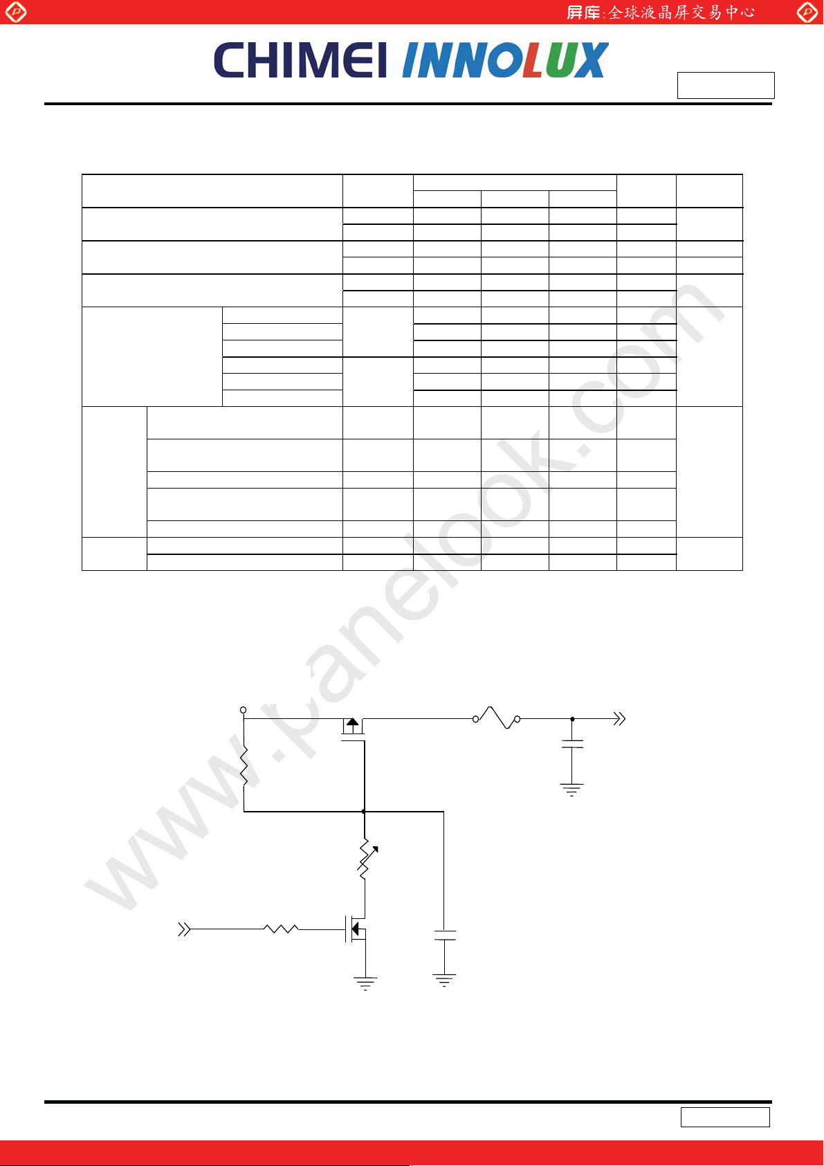
R1
1K
(Low to High)
(Control Signal)
SW
R2
1K
Q1
Si4485DY
47K
Q2
2N7002
VR1
C1
0.01uF
FUSE
C3
1uF
Vcc1 or
(LCD Module Input)
10
One step solution for LCD / PDP / OLED panel application: Datasheet, inventory and accessory!
Version 2.3
www.panelook.com
Page 11
Global LCD Panel Exchange Center
GND
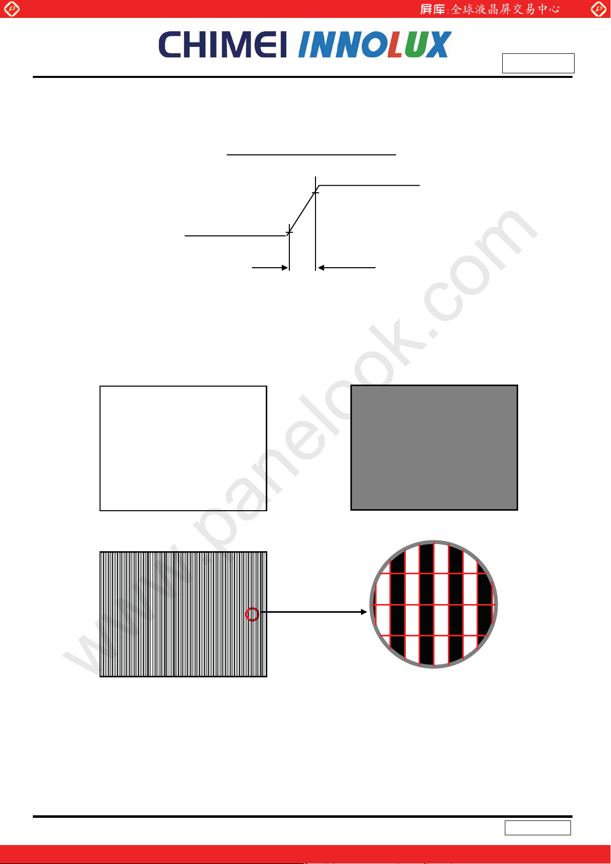
Note (3) The specified power supply current is under the conditions at Vcc1 = 18 V, Vcc2 = 5 V, Ta = 25 ± 2 ºC, fv
www.panelook.com
Issue Date:Apr.16.2010
Model No.: V562D1-L04
Approval
Vcc rising time is at least 470μs
0.9Vcc
0.1Vcc
470μs
= 60 Hz, whereas a power dissipation check pattern below is displayed.
a. White Pattern
c. Vertical Stripe Pattern
b. Black Pattern
Active Area Active Area
R
G
R
B
G
R
G
B
B
B
R
G
R
B
Active Area
R
B
R R
R
G
B
G
B
G
B
G
B
11
One step solution for LCD / PDP / OLED panel application: Datasheet, inventory and accessory!
R
Version 2.3
www.panelook.com
Page 12
Global LCD Panel Exchange Center
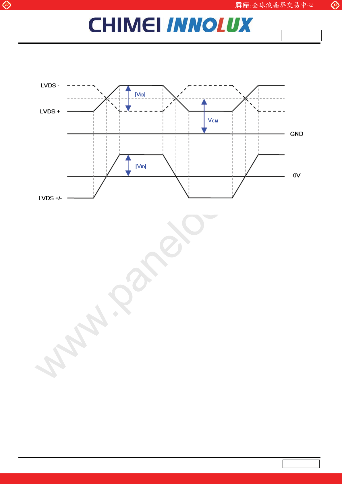
Note (4) LVDS input signal waveform
www.panelook.com
Issue Date:Apr.16.2010
Model No.: V562D1-L04
Approval
12
One step solution for LCD / PDP / OLED panel application: Datasheet, inventory and accessory!
Version 2.3
www.panelook.com
Page 13
Global LCD Panel Exchange Center
www.panelook.com
4.2. BACKLIGHT UNIT
4.2.1. CCFL (Cold Cathode Fluorescent Lamp) CHARACTERISTICS
(Ta=25±2oC)
Parameter Symbol
Lamp Voltage VW - 1728 - VRMS IL =6.0mA
Lamp Current IL 5.5 6.0 6.5 mARMS (1)
Lamp Starting Voltage VS
Operating Frequency Fo 40 60 80 KHz (3)
Lamp Life Time LBL - 50000 - Hrs (4)
Min. Typ. Max.
- - 2550 VRMS (2), Ta = 0 ºC
- - 2350 VRMS (2), Ta = 25 ºC
Value
4.2.2. INVERTER CHARACTERISTICS
(Ta=25±2oC)
Parameter Symbol
Power Consumption
Power Supply Voltage VBL 22.8 24.0 25.2 VDC
Power Supply Current IBL - 13.13 13.75 A Non Dimming
Input Ripple Noise - - - 912 mV
Oscillating Frequency FW 47 50 53 kHz
Dimming frequency FB 150 160 180 Hz
Minimum Duty Ratio D
Note (1) Lamp current is measured by utilizing AC current probe and its value is average by measuring master
PBL - 315 330 W (5), IL = 6.0mA
- 20 - %
MIN
Min. Typ. Max.
Value
Issue Date:Apr.16.2010
Model No.: V562D1-L04
Approval
Unit Note
Unit Note
VBL=22.8V
P-P
and slave board
Note (2) The lamp starting voltage VS should be applied to the lamp for more than 1 second after startup.
Otherwise the lamp may not be turned on.
Note (3) The lamp frequency may produce interference with horizontal synchronous frequency of the display
input signals, and it may result in line flow on the display. In order to avoid interference, the lamp
frequency should be detached from the horizontal synchronous frequency and its harmonics as far as
possible.
Note (4) The life time of a lamp is defined as when the brightness is larger than 50% of its original value and the
effective discharge length is longer than 80% of its original length (Effective discharge length is defined
as an area that has equal to or more than 70% brightness compared to the brightness at the center
o
point of lamp.) as the time in which it continues to operate under the condition at Ta = 25 Ʋ2
5.5 ~ 6.5mA rms.
Note (5) The power supply capacity should be higher than the total inverter power consumption PBL. Since the
pulse width modulation (PWM) mode was applied for backlight dimming, the driving current changed as
PWM duty on and off. The transient response of power supply should be considered for the changing
loading when inverter dimming.
Note (6) The measurement condition of Max. value is based on 56" backlight unit under input voltage 24V,
C and IL =
average lamp current 6.3 mA and lighting 30 minutes later.
13
One step solution for LCD / PDP / OLED panel application: Datasheet, inventory and accessory!
Version 2.3
www.panelook.com
Page 14
Global LCD Panel Exchange Center
www.panelook.com
Issue Date:Apr.16.2010
Model No.: V562D1-L04
Approval
Inverter
(Master)
a
1
2
a
a
1
2
a
a
1
2
a
a
1
2
a
a
1
2
a
a
1
2
a
a
1
2
a
a
1
2
a
HV (White -)
HV(Blue -)
HV (White +)
HV(Blue +)
HV (White -)
HV(Blue -)
HV (White +)
HV(Blue +)
HV (White -)
HV(Blue -)
HV (White +)
HV(Blue +)
HV (White -)
HV(Blue -)
HV (White +)
HV(Blue +)
A
A
A
A
A
A
A
A
A
A
A
A
A
A
A
A
HV (Pink +)
HV (White +)
HV (Pink -)
HV (White -)
HV (Pink +)
HV (White +)
HV (Pink -)
HV (White -)
HV (Pink +)
HV (White +)
HV (Pink -)
HV (White -)
HV (Pink +)
HV (White +)
HV (Pink -)
HV (White -)
A
b
1
2
A
b
1
A
b
2
A
b
1
A
b
2
A
b
A
b
1
2
A
b
A
b
1
A
b
2
A
b
1
A
b
2
1
A
b
2
A
b
A
b
1
2
A
b
Inverter
(Slave 2)
Inverter
(Slave 1)
LCD Module
a
1
2
a
1
a
2
a
1
a
2
a
a
1
2
a
a
1
2
a
a
1
2
a
a
1
2
a
1
a
2
a
HV (White -)
HV(Blue -)
HV (White +)
HV(Blue +)
HV (White -)
HV(Blue -)
HV (White +)
HV(Blue +)
HV (White -)
HV(Blue -)
HV (White +)
HV(Blue +)
HV (White -)
HV(Blue -)
HV (White +)
HV(Blue +)
A
A
A
A
A
A
A
A
A
A
A
A
A
A
A
A
HV (Pink +)
HV (White +)
HV (Pink -)
HV (White -)
HV (Pink +)
HV (White +)
HV (Pink -)
HV (White -)
HV (Pink +)
HV (White +)
HV (Pink -)
HV (White -)
HV (Pink +)
HV (White +)
HV (Pink -)
HV (White -)
A
b
1
A
b
2
A
b
1
2
A
b
A
b
1
2
A
b
A
b
1
A
b
2
A
b
1
A
b
2
A
b
1
A
b
2
A
b
1
A
b
2
A
b
1
2
A
b
Inverter
(Slave 3)
14
One step solution for LCD / PDP / OLED panel application: Datasheet, inventory and accessory!
Version 2.3
www.panelook.com
Page 15

Global LCD Panel Exchange Center
y
www.panelook.com
4.2.3. INVERTER INTERTFACE CHARACTERISTICS
Issue Date:Apr.16.2010
Model No.: V562D1-L04
Approval
Parameter Symbol
On/Off Control Voltage
Internal/External PWM
Select Voltage
Internal PWM Control
Voltage
External PWM Control
Voltage
ON
OFF
HI
LO
MAX
MIN
HI
LO 0
V
V
V
V
BLON
SEL
IPWM
EPWM
VBL Rising Time Tr1
VBL Falling Time Tf1
Control Signal Rising Time Tr
Control Signal Falling Time Tf
PWM Signal Rising Time T
PWM Signal Falling Time T
Input impedance R
PWM Delay Time T
BLON Delay Time
BLON Off Time T
PWMR
PWMF
IN
PWM
T
on
T
on1
off
Test
Condition
炼
炼
炼
炼
V
SEL
V
SEL
炼
炼
炼炼炼
炼炼炼
炼炼炼
炼炼炼
炼
炼
炼
炼
炼
= L
= H
Value
Min. Typ. Max.
2.0
0
2.0
0
炼
炼
炼
炼
5.0 V
0.8 V
5.0 V
0.8 V
Unit Note
3.15 3.3 3.45 V Note (5)
炼
2.0
30
30
0
炼
炼
炼
5.0 V dut
0.8 V duty off
炼炼
炼炼
V minimum duty ratio
on
ms
ms
100 ms
100 ms
50 us
50 us
1
100
300
300
300
炼炼 Mȟ
炼炼
炼炼
炼炼
炼炼
mS
ms
ms
ms
Note (1) The SEL signal should be valid before backlight turns on by BLON signal. It is inhibited to change the
internal/external PWM selection (SEL) during backlight turn on period.
Note (2) The power sequence and control signal timing are shown in the following figure.
Note (3) The power sequence and control signal timing must follow the figure below. For a certain reason, the
inverter has a possibility to be damaged with wrong power sequence and control signal timing.
Note (4) Abnormal operation may occur if these maximum values of control signal are exceeded.
Note (5) The range of VIPWM for dimming brightness should be constrained from 0V to 2.85V (i.e., 2.85V is the
start dimming point) except the Max. value of VIPWM mentioned here is only for the maximum brightness
useful. In other words, 2.85V~3.15V is not suggested for using to prevent from possibly abnormal
phenomenon.
Note (6) While system is turned ON or OFF, the power sequences must follow as below descriptions:
Turn ON sequence: VBL ɦ PWM signal ɦ BLON
Turn OFF sequence: BLOFF ɦ PWM signal ɦ VBL
15
One step solution for LCD / PDP / OLED panel application: Datasheet, inventory and accessory!
Version 2.3
www.panelook.com
Page 16

Global LCD Panel Exchange Center
www.panelook.com
Issue Date:Apr.16.2010
Model No.: V562D1-L04
Approval
V
VBLON
VSEL
V
EPWM
V
IPWM
9
Toff
%/
Tf1
9
%/
Tr1
BL
0
9
0
%/
2.0V
0.8V
9
Ton
%/
Ton1
Backlight on duration
Tr
Tf
2.0V
0
0.8V
Ext. Dimming Function
Int. Dimming Function
TPWMR
PWMF
2.0V
0
0.8V
T
PWM
T
3.0V
0
V
W
External
PWM
Period
External
PWM Duty
100%
Minimun
Duty
16
One step solution for LCD / PDP / OLED panel application: Datasheet, inventory and accessory!
Version 2.3
www.panelook.com
Page 17

Global LCD Panel Exchange Center
5. BLOCK DIAGRAM
5.1. TFT LCD MODULE
www.panelook.com
Issue Date:Apr.16.2010
Model No.: V562D1-L04
Approval
2B_Odd_Data0(+/-)
2B_Odd_Data1(+/-)
2B_Odd_Data2(+/-)
2B_Odd_Data3(+/-)
2B_Odd_Data4(+/-)
2B_Odd_Clock(+/-)
2B_Even_Data0(+/-)
2B_Even_Data1(+/-)
2B_Even_Data2(+/-)
2B_Even_Data3(+/-)
2B_Even_Data4(+/-)
2B_Even_Clock(+/-)
1B_Odd_Data0(+/-)
1B_Odd_Data1(+/-)
1B_Odd_Data2(+/-)
1B_Odd_Data3(+/-)
1B_Odd_Data4(+/-)
1B_Odd_Clock(+/-)
1B_Even_Data0(+/-)
1B_Even_Data1(+/-)
1B_Even_Data2(+/-)
1B_Even_Data3(+/-)
1B_Even_Data4(+/-)
1B_Even_Clock(+/-)
2A_Odd_Data0(+/-)
2A_Odd_Data1(+/-)
2A_Odd_Data2(+/-)
2A_Odd_Data3(+/-)
2A_Odd_Data4(+/-)
2A_Odd_Clock(+/-)
2A_Even_Data0(+/-)
2A_Even_Data1(+/-)
2A_Even_Data2(+/-)
2A_Even_Data3(+/-)
2A_Even_Data4(+/-)
2A_Even_Clock(+/-)
1A_Odd_Data0(+/-)
1A_Odd_Data1(+/-)
1A_Odd_Data2(+/-)
1A_Odd_Data3(+/-)
1A_Odd_Data4(+/-)
1A_Odd_Clock(+/-)
1A_Even_Data0(+/-)
1A_Even_Data1(+/-)
1A_Even_Data2(+/-)
1A_Even_Data3(+/-)
1A_Even_Data4(+/-)
1A_Even_Clock(+/-)
Vcc1
Vcc2
GND
B-F,FI-RE51S-HF,
CONNECTOR
JAE Taiwan.
INPUT
CN6
CN7
B-F,FI-RE51S-HF,
CONNECTOR
JAE Taiwan.
INPUT
CN3.
POWER
CONNECTOR
(S20B-PHDS
S-B(LF)(SN))
FRAME
BUFFER
TIMING
CONTROLLER
DC/DC CONVERTER
SCAN DRIVER
& REFERENCE
VOLTAGE
GENERATOR
DATA DRIVER (RSDS)
SCAN DRIVER
TFT LCD PANEL
(3840x3x2160)
DATA DRIVER (RSDS)
VBL
GND
SEL
E_PWM
I_PWM
BLON
VBL
GND
INVERTER
CONNECTOR
CN1:S14B-PH-SM4-TB
(D)(LF) or equivalent
(Master)
CN4,CN6: 528521070 (Molex)
INVERTER
CONNECTOR
CN2:S12B-PH-SM4-TB
(D)(LF) or equivalent
(Slave)
CN3,CN5: 528521070 (Molex)
CN8-CN23:SM02 (12.0)B-BHS-1-TB(LF)(JST)
or equivalent
BACKLIGHT
UNIT
CN5,CN7: 528521070 (Molex)
INVERTER
CONNECTOR
CN2:S12B-PH-SM4-TB
(D)(LF) or equivalent
(Slave)
INVERTER
CONNECTOR
CN2:S12B-PH-SM4-TB
(D)(LF) or equivalent
(Slave)
VBL
GND
VBL
GND
17
One step solution for LCD / PDP / OLED panel application: Datasheet, inventory and accessory!
Version 2.3
www.panelook.com
Page 18

Global LCD Panel Exchange Center
www.panelook.com
6. LCD INPUT TERMINAL PIN ASSIGNMENT
6.1. TFT LCD MODULE L.V.D.S. INPUT
CN6 Connector Pin Assignment
Pin No. Name Description Note
1 GND Ground.
2 2B_FRX0- Negative transmission data of First pixel 0.
3 2B_FRX0+ Positive transmission data of First pixel 0.
4 2B_FRX1- Negative transmission data of First pixel 1.
5 2B_FRX1+ Positive transmission data of First pixel 1.
6 2B_FRX2- Negative transmission data of First pixel 2.
7 2B_FRX2+ Positive transmission data of First pixel 2.
8 2B_ FCLK- Negative of First clock.
9 2B_ FCLK+ Positive of First clock.
10 2B_FRX3- Negative transmission data of First pixel 3.
11 2B_FRX3+ Positive transmission data of First pixel 3.
12 2B_FRX4- Negative transmission data of First pixel 4.
13 2B_FRX4+ Positive transmission data of First pixel 4.
14 2B_SRX0- Negative transmission data of Second pixel 0.
15 2B_SRX0+ Positive transmission data of Second pixel 0.
16 2B_SRX1- Negative transmission data of Second pixel 1.
17 2B_SRX1+ Positive transmission data of Second pixel 1.
18 2B_SRX2- Negative transmission data of Second pixel 2.
19 2B_SRX2+ Positive transmission data of Second pixel 2.
20 2B_ SCLK- Negative of Second clock.
21 2B_ SCLK+ Positive of Second clock.
22 2B_SRX3- Negative transmission data of Second pixel 3.
23 2B_SRX3+ Positive transmission data of Second pixel 3.
24 2B_SRX4- Negative transmission data of Second pixel 4.
25 2B_SRX4+ Positive transmission data of Second pixel 4.
26 GND Ground.
27 2A_FRX0- Negative transmission data of First pixel 0.
28 2A_FRX0+ Positive transmission data of First pixel 0.
29 2A_FRX1- Negative transmission data of First pixel 1.
30 2A_FRX1+ Positive transmission data of First pixel 1.
31 2A_FRX2- Negative transmission data of First pixel 2.
32 2A_FRX2+ Positive transmission data of First pixel 2.
33 2A_ FCLK- Negative of First clock.
34 2A_ FCLK+ Positive of First clock.
35 2A_FRX3- Negative transmission data of First pixel 3.
36 2A_FRX3+ Positive transmission data of First pixel 3.
37 2A_FRX4- Negative transmission data of First pixel 4.
38 2A_FRX4+ Positive transmission data of First pixel 4.
39 2A_SRX0- Negative transmission data of Second pixel 0.
40 2A_SRX0+ Positive transmission data of Second pixel 0.
41 2A_SRX1- Negative transmission data of Second pixel 1.
42 2A_SRX1+ Positive transmission data of Second pixel 1.
43 2A_SRX2- Negative transmission data of Second pixel 2.
44 2A_SRX2+ Positive transmission data of Second pixel 2.
45 2A_ SCLK- Negative of Second clock.
46 2A_ SCLK+ Positive of Second clock.
Issue Date:Apr.16.2010
Model No.: V562D1-L04
Approval
18
One step solution for LCD / PDP / OLED panel application: Datasheet, inventory and accessory!
Version 2.3
www.panelook.com
Page 19

Global LCD Panel Exchange Center
47 2A_SRX3- Negative transmission data of Second pixel 3.
48 2A_SRX3+ Positive transmission data of Second pixel 3.
49 2A_SRX4- Negative transmission data of Second pixel 4.
50 2A_SRX4+ Positive transmission data of Second pixel 4.
51 GND Ground.
CN7 Connector Pin Assignment
Pin No. Name Description Note
1 GND Ground.
2 1B_FRX0- Negative transmission data of First pixel 0.
3 1B_FRX0+ Positive transmission data of First pixel 0.
4 1B_FRX1- Negative transmission data of First pixel 1.
5 1B_FRX1+ Positive transmission data of First pixel 1.
6 1B_FRX2- Negative transmission data of First pixel 2.
7 1B_FRX2+ Positive transmission data of First pixel 2.
8 1B_ FCLK- Negative of First clock.
9 1B_ FCLK+ Positive of First clock.
10 1B_FRX3- Negative transmission data of First pixel 3.
11 1B_FRX3+ Positive transmission data of First pixel 3.
12 1B_FRX4- Negative transmission data of First pixel 4.
13 1B_FRX4+ Positive transmission data of First pixel 4.
14 1B_SRX0- Negative transmission data of Second pixel 0.
15 1B_SRX0+ Positive transmission data of Second pixel 0.
16 1B_SRX1- Negative transmission data of Second pixel 1.
17 1B_SRX1+ Positive transmission data of Second pixel 1.
18 1B_SRX2- Negative transmission data of Second pixel 2.
19 1B_SRX2+ Positive transmission data of Second pixel 2.
20 1B_ SCLK- Negative of Second clock.
21 1B_ SCLK+ Positive of Second clock.
22 1B_SRX3- Negative transmission data of Second pixel 3.
23 1B_SRX3+ Positive transmission data of Second pixel 3.
24 1B_SRX4- Negative transmission data of Second pixel 4.
25 1B_SRX4+ Positive transmission data of Second pixel 4.
26 GND Ground.
27 1A_FRX0- Negative transmission data of First pixel 0.
28 1A_FRX0+ Positive transmission data of First pixel 0.
29 1A_FRX1- Negative transmission data of First pixel 1.
30 1A_FRX1+ Positive transmission data of First pixel 1.
31 1A_FRX2- Negative transmission data of First pixel 2.
32 1A_FRX2+ Positive transmission data of First pixel 2.
33 1A_ FCLK- Negative of First clock.
34 1A_ FCLK+ Positive of First clock.
35 1A_FRX3- Negative transmission data of First pixel 3.
36 1A_FRX3+ Positive transmission data of First pixel 3.
37 1A_FRX4- Negative transmission data of First pixel 4.
38 1A_FRX4+ Positive transmission data of First pixel 4.
39 1A_SRX0- Negative transmission data of Second pixel 0.
40 1A_SRX0+ Positive transmission data of Second pixel 0.
41 1A_SRX1- Negative transmission data of Second pixel 1.
42 1A_SRX1+ Positive transmission data of Second pixel 1.
43 1A_SRX2- Negative transmission data of Second pixel 2.
www.panelook.com
Issue Date:Apr.16.2010
Model No.: V562D1-L04
Approval
19
One step solution for LCD / PDP / OLED panel application: Datasheet, inventory and accessory!
Version 2.3
www.panelook.com
Page 20

Global LCD Panel Exchange Center
44 1A_SRX2+ Positive transmission data of Second pixel 2.
45 1A_ SCLK- Negative of Second clock.
46 1A_ SCLK+ Positive of Second clock.
47 1A_SRX3- Negative transmission data of Second pixel 3.
48 1A_SRX3+ Positive transmission data of Second pixel 3.
49 1A_SRX4- Negative transmission data of Second pixel 4.
50 1A_SRX4+ Positive transmission data of Second pixel 4.
51 GND Ground.
Note (1) CN6&CN7 connector part no.: B-F,FI-RE51S-HF,JAE Taiwan.
6.2. TFT LCD MODULE POWER INPUT
CN3 Connector Pin Assignment
Pin No. Symbol Description Note
1 VIN +18.0V power supply
2 VIN +18.0V power supply
3 V5VC +5.0V power supply
4 V5VC +5.0V power supply
5 V5VC +5.0V power supply
6 NC Not connection
7 V5VC +5.0V power supply
8 NC Not connection
9 V5VC +5.0V power supply
10 NC Not connection
11 GND Ground
12 NC Not connection
13 GND Ground
14 NC Not connection
15 GND Ground
16 ODSEL Overdrive Lookup Table Selection (2)(3)
17 GND Ground
18 GND Ground
19 GND Ground
20 GND Ground
Note (1) CN3 connector part no.: S20B-PHDSS-B(LF)(SN), JST(㖍㛔⡻叿䪗⫸),⽟忂䪗⫸ or equivalent.
www.panelook.com
Issue Date:Apr.16.2010
Model No.: V562D1-L04
Approval
Note (2) ODSEL (Overdrive Lookup Table Selection). The overdrive lookup table should be selected in
accordance to the frame rate to optimize image quality.
ODSEL Note
L Lookup table was optimized for 60Hz frame rate.
H Lookup table was optimized for 50Hz frame rate.
Note (3) “L” and “H” operation in (3) could follow “CMOS Interface” in Section 4.1
20
One step solution for LCD / PDP / OLED panel application: Datasheet, inventory and accessory!
Version 2.3
www.panelook.com
Page 21

Global LCD Panel Exchange Center
6.3. BACKLIGHT UNIT
The pin configuration for the housing and the leader wire is shown in the table below.
Pin Name Description Wire Color
1 HV High Voltage Pink
2 HV High Voltage White
Note (1) The backlight interface housing for high voltage side is a model BHR-04VS-1, manufactured by JST and
the mating header on inverter part number is SM02 (12.0) B-BHS-1-TB (LF).
1 HV(White)
2 HV(Pink)
www.panelook.com
CN8-CN23: BHR-04VS-1 (JST).
Issue Date:Apr.16.2010
Model No.: V562D1-L04
Approval
1 HV(Pink)
2 HV(White)
˕
˕
˕
˕
1
1
2
2
1 HV(White)
2 HV(Pink)
1 HV(White)
2 HV(Pink)
1 HV(Pink)
2 HV(White)
1 HV(Pink)
2 HV(White)
31
˕
32
˕
21
One step solution for LCD / PDP / OLED panel application: Datasheet, inventory and accessory!
Version 2.3
www.panelook.com
Page 22

Global LCD Panel Exchange Center
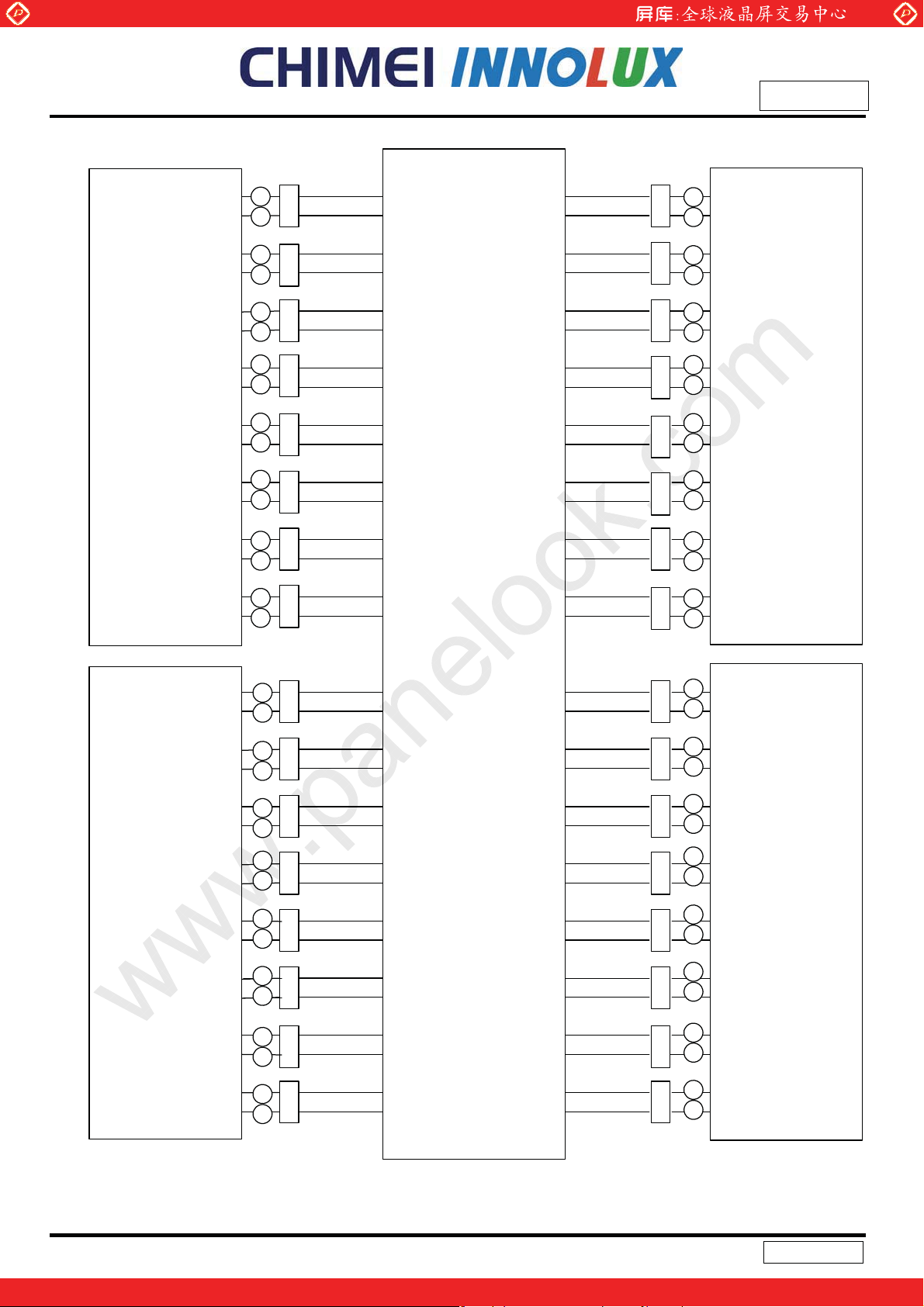
6.4. INVERTER UNIT
CN1 (Master, Header): S14B-PH-SM4-TB (D)(LF)(JST) or equivalent
Pin No. Symbol Description
1
2
3
4
5
6
7
8
9
10
11 SEL
12 E_PWM External PWM control signal
13 I_PWM Internal PWM Control Signal
14 BLON Backlight on/off control
VBL +24V
GND GND
Internal/External PWM selection
High : external dimming
Low : internal dimming
power input
DC
www.panelook.com
Issue Date:Apr.16.2010
Model No.: V562D1-L04
Approval
CN2 (Slave, Header): S12B-PH-SM4-TB (D)(LF)(JST) or equivalent
Pin No. Symbol Description
1
2
3
4
5
6
7
8
9
10
11 NC NC
12 NC NC
CN8-CN15 (Master, Header), CN16-CN23 (Slave, Header): SM02 (12.0) B-BHS-1-TB (LF)(JST) or equivalent
Pin No. Symbol Description
1
2
VBL +24V
GND GND
CCFL HOT
CCFL HOT
CCFL high voltage
CCFL high voltage
power input
DC
22
One step solution for LCD / PDP / OLED panel application: Datasheet, inventory and accessory!
Version 2.3
www.panelook.com
Page 23

Global LCD Panel Exchange Center
CN3-CN4 (Master, Header), CN5-CN7 (Slave, Header): 528521070 (Molex)
Pin No. Symbol Description
1
2 Board to Board
3 Board to Board
4 Board to Board
5 Board to Board
6 Board to Board
7 Board to Board
8 Board to Board
9 Board to Board
10 Board to Board
Note (1) Floating of any control signal is not allowed.
Control
Signal
Board to Board
www.panelook.com
Issue Date:Apr.16.2010
Model No.: V562D1-L04
Approval
23
One step solution for LCD / PDP / OLED panel application: Datasheet, inventory and accessory!
Version 2.3
www.panelook.com
Page 24

Global LCD Panel Exchange Center
6.5. BLOCK DIAGRAM OF IMAGE SIGNAL
The video picture (3840x2160) should be divided into four parts: the left up side (1920x1080), the left down side
(1920x1080), the right up side (1920x1080) and the right down side (1920x1080). Signals of these four parts
should be delivered into the module individually through each 2-channel LVDS interface. But it must be
“synchronous” mutually between signals from these four 2-channel LVDS interfaces. And the protocol is specified
in the LVDS interface specification.
www.panelook.com
Issue Date:Apr.16.2010
Model No.: V562D1-L04
Approval
CN3
CC Board
CN6
Note (1) It must be “synchronous” mutually between signals from CN6(2A) and CN6(2B).
Note (2) It must be “synchronous” mutually between signals from CN7(1A) and CN7(1B).
Note (3) It exists 1/3 frame buffer (i.e. buffer =1/3 x 1920 x1080 pixels) between CN6 and CN7.
24
CN7
One step solution for LCD / PDP / OLED panel application: Datasheet, inventory and accessory!
Version 2.3
www.panelook.com
Page 25

Global LCD Panel Exchange Center
6.6. BLOCK DIAGRAM OF L.V.D.S.
FRX0+
www.panelook.com
Issue Date:Apr.16.2010
Model No.: V562D1-L04
Approval
FRX0-
FRX1+
FRX1-
FRX2+
FRX2-
FRX3+
FRX3-
FRX4+
FRX4-
FCLK+
FCLK-
SRX0+
Rx-OUT
FR0-FR9
FG0-FG9
FB0-FB9
DE
SR0-SR9
SG0-SG9
SB0-SB9
DCLK
PLL
Timing Controller
SRX0-
SRX1+
SRX1-
SRX2+
SRX2-
SRX3+
SRX3-
SRX4+
SRX4-
SCLK+
SCLK-
LVDS Input
PLL
LVDS Receiver
25
One step solution for LCD / PDP / OLED panel application: Datasheet, inventory and accessory!
Version 2.3
www.panelook.com
Page 26

Global LCD Panel Exchange Center
FR0~FR9 : First pixel R data
FG0~FG9 : First pixel G data
FB0~FB9 : First pixel B data
SR0~SR9 : Second pixel R data
SG0~SG9 : Second pixel G data
SB0~SB9 : Second pixel B data
DE : Data enable signal
DCLK : Data clock signal
Note (1) The driving system must have the transmitter to drive the module.
Note (2) LVDS cable impedance shall be 50 ohms per signal line or about 100 ohms per twist-pair line when it is
used differentially.
www.panelook.com
Issue Date:Apr.16.2010
Model No.: V562D1-L04
Approval
Note (3) Two pixel data are sent into the module for every clock cycle.
26
One step solution for LCD / PDP / OLED panel application: Datasheet, inventory and accessory!
Version 2.3
www.panelook.com
Page 27

Global LCD Panel Exchange Center
6.7. L.V.D.S. INTERFACE
www.panelook.com
Issue Date:Apr.16.2010
Model No.: V562D1-L04
Approval
R0~R9 : Pixel R Data (9; MSB, 0; LSB)
G0~G9 : Pixel G Data (9; MSB, 0; LSB)
B0~B9 : Pixel B Data (9; MSB, 0; LSB)
DE : Data enable signal
RCLK : Data clock signal
Note (1) RSVD (reserved)pins on the transmitter shall be “H” or “L”.
27
One step solution for LCD / PDP / OLED panel application: Datasheet, inventory and accessory!
Version 2.3
www.panelook.com
Page 28

Global LCD Panel Exchange Center
6.8. COLOR DATA INPUT ASSIGNMENT
The brightness of each primary color (red, green and blue) is based on the 10-bit gray scale data input for the color.
The higher the binary input the brighter the color. The table below provides the assignment of color versus data
input.
www.panelook.com
Issue Date:Apr.16.2010
Model No.: V562D1-L04
Approval
Basic
Colors
Gray
Scale
Of
Red
Gray
Scale
Of
Green
Gray
Scale
Of
Blue
Color
Black
Red
Green
Blue
Cyan
Magenta
Yellow
White
Red (0) / Dark
Red (1)
Red (2)
:
:
Red (1021)
Red (1022)
Red (1023)
Green (0) / Dark
Green (1)
Green (2)
:
:
Green (1021)
Green (1022)
Green (1023)
Blue (0) / Dark
Blue (1)
Blue (2)
:
:
Blue (1021)
Blue (1022)
Blue (1023)
0
0
1
0
1
0
1
1
0
0
0
:
:
0
0
0
0
0
0
:
:
1
1
1
0
0
0
:
:
0
0
0
Data Signal
0
0
0
0
1
1
0
0
1
1
0
0
1
1
1
1
0
0
0
0
0
0
:
:
:
:
0
0
0
0
0
0
0
0
0
0
0
0
:
:
:
:
1
1
1
1
1
1
0
0
0
0
0
0
:
:
:
:
0
0
0
0
0
0
0
0
0
0
0
0
0
0
0
0
1
1
1
0
0
0
1
1
1
0
0
0
1
1
1
1
1
1
0
0
0
0
0
0
0
0
0
:
:
:
:
:
:
0
0
0
0
0
0
0
0
0
0
0
0
0
0
0
0
0
0
:
:
:
:
:
:
1
1
1
1
1
1
1
1
1
0
0
0
0
0
0
0
0
0
:
:
:
:
:
:
0
0
0
0
0
0
0
0
0
0
0
0
0
1
1
1
0
0
0
1
1
1
0
0
0
1
1
1
1
1
1
0
0
0
0
0
0
0
0
0
:
:
:
:
:
:
0
0
0
0
0
0
0
0
0
0
0
0
1
0
0
0
0
1
:
:
:
:
:
:
1
0
1
0
1
1
1
1
1
0
0
0
0
0
0
0
0
0
:
:
:
:
:
:
0
0
0
0
0
0
0
0
0
0
0
0
0
0
0
0
0
0
1
1
1
1
1
1
1
1
1
0
0
0
1
1
1
0
0
0
0
0
0
0
0
0
:
:
:
:
:
;
0
0
0
0
0
0
0
0
0
0
0
0
0
0
0
0
0
0
:
:
:
:
:
:
0
0
0
0
0
0
0
0
0
0
0
0
0
0
0
0
0
0
:
:
:
:
:
:
1
1
1
1
1
1
1
1
1
0
0
0
0
0
0
0
1
1
1
1
1
1
1
1
1
0
0
0
1
1
1
0
0
0
0
0
0
0
0
0
:
:
:
:
:
:
0
0
0
0
0
0
0
0
0
0
0
0
0
0
0
0
0
0
:
:
:
:
:
:
0
0
0
0
0
0
0
0
0
0
0
0
0
0
0
0
0
0
:
:
:
:
:
:
1
1
1
1
1
1
1
1
1
0
0
0
0
0
0
0
0
0
1
1
1
1
1
1
1
1
1
0
0
0
1
1
1
0
0
0
0
0
0
0
0
0
:
:
:
:
:
:
0
0
0
0
0
0
0
0
0
0
0
0
0
0
0
0
0
0
:
:
:
:
:
:
0
0
0
0
0
0
0
0
0
0
0
0
0
0
0
0
0
1
:
:
:
:
:
:
1
1
0
1
1
1
1
1
1
R9 R8 R7 R6 R5 R4 R3 R2 R1 R0 G9 G8 G7 G6 G5 G4 G3 G2 G1 G0 B9 B8 B7 B6 B5 B4 B3 B2 B1 B0
0
0
1
1
0
0
0
0
0
0
1
1
1
1
1
1
0
0
0
0
0
0
1
1
1
1
1
1
0
0
0
0
0
0
:
:
:
:
0
0
0
0
0
0
0
0
0
0
0
0
:
:
:
:
0
0
0
0
0
0
Red Green Blue
0
0
0
0
0
0
1
1
0
0
0
0
0
0
1
1
1
1
1
1
0
0
0
0
0
0
:
:
:
:
1
1
1
1
1
1
0
0
0
0
0
0
:
:
:
:
0
0
0
0
0
0
0
0
0
0
0
0
:
:
:
:
0
0
0
0
0
0
0
0
0
1
1
1
1
0
0
0
0
0
0
0
0
0
0
0
0
1
1
1
1
1
1
0
0
0
:
:
1
1
1
0
0
0
:
:
0
0
0
0
0
0
:
:
0
0
0
1
1
1
1
1
1
0
0
0
0
0
0
0
0
0
:
:
:
:
:
:
1
1
1
1
1
1
1
1
1
0
0
0
0
0
0
0
0
0
:
:
:
:
:
:
0
0
0
0
0
0
0
0
0
0
0
0
0
0
0
0
0
0
:
:
:
:
:
:
0
0
0
0
0
0
0
0
0
0
1
1
1
0
0
0
0
0
1
0
0
0
1
1
1
1
1
1
1
1
0
0
0
0
1
0
0
0
1
:
:
:
:
:
:
0
1
0
0
0
1
0
1
1
0
0
0
0
0
0
0
0
0
:
:
:
:
:
:
0
0
1
0
0
1
0
0
1
0
0
0
0
0
0
0
0
0
:
:
:
:
:
:
0
0
0
0
0
0
0
0
0
0
0
0
1
1
1
0
1
0
0
0
:
:
0
0
0
0
0
0
:
:
0
0
0
0
1
0
:
:
1
0
1
Note (1) 0: Low Level Voltage, 1: High Level Voltage
28
One step solution for LCD / PDP / OLED panel application: Datasheet, inventory and accessory!
Version 2.3
www.panelook.com
Page 29

Global LCD Panel Exchange Center
www.panelook.com
7. TIMING REQUIREMENTS OF IMAGE SIGNAL
7.1. INPUT SIGNAL TIMING SPECIFICATIONS
The input signal timing specifications are shown as the following table and timing diagram.
Signal Item Symbol Min. Typ. Max. Unit Note
LVDS Receiver Clock
(1-CH LVDS)
LVDS Receiver Data
Vertical Active Display Term
(2-CH LVDS,1920X1080 Active Area)
Horizontal Active Display Term
(2-CH LVDS, 1920x1080 Active Area)
Note (1) Since this module is operated in DE only mode, Hsync and Vsync input signals should be set to low logic
Frequency 1/Tc 60 74 75 MHZ (1)
Input cycle to
cycle jitter
Setup Time Tlvsu 600 - - ps
Hold Time Tlvhd 600 - - ps
Frame Rate
Total Tv 1115 1125 1139 Th Tv=Tvd+Tvb
Display Tvd - 1080 - Th
Blank Tvb 35 45 55 Th
Total Th 2190 2200 2300 Tc Th=Thd+Thb
Display Thd - 1920 - Tc
Blank Thb 270 280 380 Tc
Issue Date:Apr.16.2010
Model No.: V562D1-L04
Approval
Trcl - - 200 ps
5
47 50 53 Hz (2)
Fr
Fr6 57 60 60 Hz (3)
level. Otherwise, this module would operate abnormally.
Note (2) (ODSEL) = (H). Please refer to Section 6.2 for detail information.
Note (3) (ODSEL) = (L). Please refer to Section 6.2 for detail information.
INPUT SIGNAL TIMING DIAGRAM
T
v
T
vd
DE
T
h
DCLK
焍
焍
T
c
T
T
hb
hd
T
vb
焍
焍
DE
DATA
Valid display data (960 DCLK)
29
One step solution for LCD / PDP / OLED panel application: Datasheet, inventory and accessory!
Version 2.3
www.panelook.com
Page 30

Global LCD Panel Exchange Center
RXCLK+/-
RXn+/-
www.panelook.com
Issue Date:Apr.16.2010
Model No.: V562D1-L04
Approval
LVDS RECEIVER TIMING DIAGRAM
Tc
Tlvsu
Tlvhd
1T
14
3T
14
5T
14
7T
14
9T
14
11T
14
13T
14
30
One step solution for LCD / PDP / OLED panel application: Datasheet, inventory and accessory!
Version 2.3
www.panelook.com
Page 31

Global LCD Panel Exchange Center
7.2. POWER ON/OFF SEQUENCE
To prevent a latch-up or DC operation of LCD module, the power on/off sequence should be followed as the
diagram below.
őŰŸŦųġŔŶűűŭź
őŰŸŦųġŔŶűűŭź
őŰŸŦųġŔŶűűŭźőŰŸŦųġŔŶűűŭź
ŗŤŤIJĭġŗŤŤij
www.panelook.com
ıįĺŗŤŤIJ
Issue Date:Apr.16.2010
Model No.: V562D1-L04
Approval
ıįĺŗŤŤIJ
ıįĶʀŕIJʀIJıŮŴĩŗŤŤIJĪ
ıįĶʀŕĸʀIJıŮŴĩŗŤŤijĪ
ıʀŕĹʀĶıŮŴ
ıʀŕijʀĶıŮŴ
ıʀŕĴʀĶıŮŴ
ĶııŮŴʀŕĵ
ŔŪŨůŢŭŴ
ŔŪŨůŢŭŴ
ŔŪŨůŢŭŴŔŪŨůŢŭŴ
ŃŢŤŬŭŪŨũŵġĩœŦŤŰŮŮŦůťŦťĪ
IJĶııŮŴʀŕĶ
IJııŮŴʀŕķ
ıŗ
ıŗ
ıŗ
ıįIJŗŤŤIJ
ŕIJ
ŕIJ
ŕIJŕIJ
ıįĺŗŤŤij
ıįIJŗŤŤij
ŕĹ
ŕĹ
ŕĹŕĹ
ŕĸ
ŕĸ
ŕĸŕĸ
ŕij
ŕij
ŕijŕij
ıįĺŗŤŤij
ŕĴ
ŕĴ
ŕĴŕĴ
ŗłōŊŅ
őŰŸŦųġŐů őŰŸŦųġŐŧŧ
ĶıĦ ĶıĦ
ŕĶ
ŕĶ ŕķ
ŕĶŕĶ
őŰŸŦųġŐŏİŐŇŇġŔŦŲŶŦůŤŦ
őŰŸŦųġŐŏİŐŇŇġŔŦŲŶŦůŤŦ
őŰŸŦųġŐŏİŐŇŇġŔŦŲŶŦůŤŦőŰŸŦųġŐŏİŐŇŇġŔŦŲŶŦůŤŦ
ŕķ
ŕķŕķ
ıįIJŗŤŤIJ
ıįIJŗŤŤij
ŕĵ
ŕĵ
ŕĵŕĵ
Note (1) The supplied voltage of the external system for the module input should follow the definition of Vcc1,2.
Note (2) Apply the lamp voltage within the LCD operation range. When the backlight turns on before the LCD
operation or the LCD turns off before the backlight turns off, the display may momentarily become
abnormal screen.
Note (3) In case of Vcc1,2 is in off level, please keep the level of input signals on the low and avoid floating.
Note (4) T4 should be measured after the module being fully discharged between power off and on period.
Note (5) Interface signal shall not be kept at high impedance when the power is on.
31
One step solution for LCD / PDP / OLED panel application: Datasheet, inventory and accessory!
Version 2.3
www.panelook.com
Page 32

Global LCD Panel Exchange Center
8. OPTICAL CHARACTERISTICS
8.1. TEST CONDITIONS
Item Symbol Value Unit
Ambient Temperature Ta
Ambient Humidity Ha
Supply Voltage VCC 5.0 V
Input Signal According to typical value in "3. ELECTRICAL CHARACTERISTICS"
Frame Rate Fr 60 Hz
8.2. OPTICAL SPECIFICATIONS
The relative measurement methods of optical characteristics are shown in 8.2 Notes. The following items should
be measured under the test conditions described in 8.1 and stable environment shown in Note (6).
Item Symbol Condition Min. Typ. Max. Unit Note
Contrast Ratio CR
Response Time
Center Luminance of White L
Average Luminance of White L
White Variation
Cross Talk CT 2 % Note (5)
Red
Green
Color
Chromaticity
Blue
White
Color Gamut C.G 95 100 % NTSC
Horizontal
Viewing
Angle
Vertical
Gray to
gray
www.panelook.com
Issue Date:Apr.16.2010
Model No.: V562D1-L04
Approval
o
25±2
50±10
900 1200 - Note (2)
6.5 12 ms Note (3)
C
400 450 - cd/m2Note (4)
AVE
δW
=0°, θY =0°
θ
Rx
Ry
x
Viewing angle at
normal direction
Gx
Gy
Bx
By
Wx
Wy
θ
+
x
θx-
θ
+
Y
CR≥30
θY-
400 450 cd/m2Note (4)
1.6 - Note (7)
0.663
0.330
0.184
Typ.
-0.03
0.691
0.149
Typ.
+0.03
0.050
0.313
0.329
80 88
80 88
80 88
80 88
C
%RH
-
-
-
-
-
-
-
-
Deg. Note (1)
Note (6)
32
One step solution for LCD / PDP / OLED panel application: Datasheet, inventory and accessory!
Version 2.3
www.panelook.com
Page 33

Global LCD Panel Exchange Center
Note (1) Definition of Viewing Angle (θx, θy):
Viewing angles are measured by Autronic Conoscope Cono-80
www.panelook.com
Issue Date:Apr.16.2010
Model No.: V562D1-L04
Approval
Normal
θx = θy = 0º
θy- θy+
θX- = 90º
x-
θx−
12 o’clock direction
y+
y+
= 90º
θ
θx+
6 o’clock
y-
= 90º
θ
y-
x+
θX+ = 90º
Note (2) Definition of Contrast Ratio (CR):
The contrast ratio can be calculated by the following expression.
Contrast Ratio (CR) = L1023 / L0
L1023: Luminance of gray level 1023
L 0: Luminance of gray level 0
CR = CR (7), where CR (X) is corresponding to the Contrast Ratio of the point X at the figure in Note (7).
Note (3) Definition of Gray to Gray Switching Time:
Time
100%
90%
Optical
Response
10%
0%
Time
Gray to gray
switching time
Gray to gray
switching time
The driving signal means the signal of gray level 0, 124, 252, 380, 508, 636, 764, 892, and 1023.Gray to
gray. Average time means the average switching time of gray level 0, 124, 252, 380, 508, 636, 764, 892,
and 1023 to each other.
33
Version 2.3
One step solution for LCD / PDP / OLED panel application: Datasheet, inventory and accessory!
www.panelook.com
Page 34

Global LCD Panel Exchange Center
(
)
(
)
(
)
Note (4) Definition of Luminance of White (LC, LAVE):
Measure the luminance of gray level 1023 at center point and 5 points
www.panelook.com
Issue Date:Apr.16.2010
Model No.: V562D1-L04
Approval
L
L
= L (7)
C
= [L (4)+ L (5)+ L (7)+ L (9)+ L (10)] / 5
AVE
Where L (x) is corresponding to the luminance of the point X at the figure in Note (7).
Note (5) Definition of Cross Talk (CT):
CT = | Y
– YA | / YA× 100 (%)
B
Where:
Y
Y
Y
(D/8,W/2)
A, L
Y
(D/2,7W/8)
A, D
= Luminance of measured location without gray level 1023 pattern (cd/m2)
A
= Luminance of measured location with gray level 1023 pattern (cd/m2)
B
(0, 0)
Active Area
Gray 512
Y
(D/2,W/8)
A, U
Y
(7D/8,W/2)
A, R
D,W
(D/8,W/8)
(D/4,W/4)
Y
(D/8,W/2)
B, L
(D/8,5W/8)
(D/2,7W/8)
Y
B, D
0, 0
Active Area
Gray 512
(3D/8,7W/8)
Gray 1023
Y
D,W
Y
(D/2,W/8)
B, U
(7D/8,W/2)
B, R
(3D/4,3W/4)
34
One step solution for LCD / PDP / OLED panel application: Datasheet, inventory and accessory!
Version 2.3
www.panelook.com
Page 35

Global LCD Panel Exchange Center
Note (6) Measurement Setup:
The LCD module should be stabilized at given temperature for 1 hour to avoid abrupt temperature
change during measuring. In order to stabilize the luminance, the measurement should be executed after
lighting backlight for 1 hour in a windless room.
www.panelook.com
Issue Date:Apr.16.2010
Model No.: V562D1-L04
Approval
Note (7) Definition of White Variation (δW):
Measure the luminance of gray level 512 at 13 points
δW = Maximum [L (1), L (2), L (3), L (4),ˣˣˣ, L (13)] / Minimum [L (1), L (2), L (3), L (4),ˣˣˣ, L (13)]
D
3D/10 5D/10 7D/10
2
4
7
W
W/10
3W/10
5W/10
D/10 9D/10
1
6
Vertical Line
7W/10
9W/10
11
9
12
Active Area
10
3
5
X
8
13
: Test Point
X=1 to 13
35
One step solution for LCD / PDP / OLED panel application: Datasheet, inventory and accessory!
Version 2.3
www.panelook.com
Page 36

Global LCD Panel Exchange Center
www.panelook.com
9. PRECAUTIONS
9.1. ASSEMBLY AND HANDLING PRECAUTIONS
(1) Do not apply rough force such as bending or twisting to the module during assembly.
(2) It is recommended to assemble or to install a module into the user’s system in clean working areas. The dust
and oil may cause electrical short or worsen the polarizer.
(3) Do not apply pressure or impulse to the module to prevent the damage of LCD panel and Backlight.
(4) Always follow the correct power-on sequence when the LCD module is turned on. This can prevent the
damage and latch-up of the CMOS LSI chips.
(5) Do not plug in or pull out the I/F connector while the module is in operation.
(6) Do not disassemble the module.
(7) Use a soft dry cloth without chemicals for cleaning, because the surface of polarizer is very soft and easily
scratched.
Issue Date:Apr.16.2010
Model No.: V562D1-L04
Approval
(8) Moisture can easily penetrate into LCD module and may cause the damage during operation.
(9) When storing modules as spares for a long time, the following precaution is necessary.
a. Do not leave the module in high temperature, and high humidity for a long time.It is highly
recommended to store the module with temperature from 0 to 35 ºC at normal humidity without
condensation.
b. The module shall be stored in dark place. Do not store the TFT-LCD module in direct sunlight or
fluorescent light.
(10) When ambient temperature is lower than 10 ºC, the display quality might be reduced. For example, the
response time will become slow, and the starting voltage of CCFL will be higher than that of room temperature.
9.2. SAFETY PRECAUTIONS
(1) The startup voltage of a Backlight is approximately 1000 Volts. It may cause an electrical shock while
assembling with the inverter. Do not disassemble the module or insert anything into the Backlight unit.
(2) If the liquid crystal material leaks from the panel, it should be kept away from the eyes or mouth. In case of
contact with hands, skin or clothes, it has to be washed away thoroughly with soap.
(3) After the module’s end of life, it is not harmful in case of normal operation and storage.
9.3. SAFETY STANDARDS
The LCD module should be certified with safety regulations as follows:
(1) UL60950-1 or updated standard.
(2) IEC60950-1 or updated standard.
(3) UL60065 or updated standard.
(4) IEC60065 or updated standard.
36
One step solution for LCD / PDP / OLED panel application: Datasheet, inventory and accessory!
Version 2.3
www.panelook.com
Page 37

Global LCD Panel Exchange Center
10. DEFINITION OF LABELS
10.1. CMO MODULE LABEL
The barcode nameplate is pasted on each module as illustration, and its definitions are as following explanation.
V562D1 -L04 Rev. XX
www.panelook.com
Issue Date:Apr.16.2010
Model No.: V562D1-L04
Approval
CHI MEI
OPTOELECTRONICS
1. Model Name: V562D1-L04
2. Revision: Rev. XX, for example: A0, A1… B1, B2… or C1, C2…etc.
3. Serial ID: X X
Serial ID includes the information as below:
X X X X X Y M D L N N N N
X X X X X X X Y M D L N N N N
Serial No.
Product Line
Year, Month, Date
CMO Internal Use
CMO Internal Use
Revision
CMO Internal Use
RoHS GEMN
(a) Manufactured Date: Year: 0~9, for 2000~2009
Month: 1~9, A~C, for Jan. ~ Dec.
st
Day: 1~9, A~Y, for 1
(b) Revision Code: Cover all the change
(c) Serial No.: Manufacturing sequence of product
(d) Product Line: 1 -> Line1, 2 -> Line 2, …etc.
to 31st, exclude I ,O, and U.
37
One step solution for LCD / PDP / OLED panel application: Datasheet, inventory and accessory!
Version 2.3
www.panelook.com
Page 38

Global LCD Panel Exchange Center
10.2. WARRANTY LABEL
Warranty labels are pasted on the rear of the BLU. This warranty label is defined to recognized if the module ever
disassembled or not. If the module was dismounted, then it will be out of warranty. When remove the warranty
label, there are prints will remain on the surface of the BLU.If the label was removed or it has the imprint by
tearing , it will be treated as disassembled.
www.panelook.com
Issue Date:Apr.16.2010
Model No.: V562D1-L04
Approval
38
One step solution for LCD / PDP / OLED panel application: Datasheet, inventory and accessory!
Version 2.3
www.panelook.com
Page 39

Global LCD Panel Exchange Center
11. PACKAGING
11.1. PACKING SPECIFICATIONS
(1) 2 LCD TV modules / 1 Box
(2) Box dimensions : 1448(L) X 372 (W) X 901 (H)
(3) Weight : approximately 56Kg (2 modules per box)
(4) One protective film is attached on the LCD TV
11.2. PACKING METHOD
Figures 11-1 and 11-2 are the packing method
LCD TV Module
www.panelook.com
Issue Date:Apr.16.2010
Model No.: V562D1-L04
Approval
Cushion(Bottom)
Anti-static Bag
Carton
Carton Label
4pcs Joint
Figure.11-1 packing method
39
One step solution for LCD / PDP / OLED panel application: Datasheet, inventory and accessory!
Version 2.3
www.panelook.com
Page 40

Global LCD Panel Exchange Center
Sea / Land Transportation
B
(40ft / 40ft HQ Container)
www.panelook.com
Air Transportation
B
Issue Date:Apr.16.2010
Model No.: V562D1-L04
Approval
Figure.11-2 Packing method
40
One step solution for LCD / PDP / OLED panel application: Datasheet, inventory and accessory!
Version 2.3
www.panelook.com
Page 41

Global LCD Panel Exchange Center
12. MECHANICAL CHARACTERISTIC
www.panelook.com
Issue Date:Apr.16.2010
Model No.: V562D1-L04
Approval
⣯伶暣⫸偉ấ㚱旸℔⎠
CHI MEI
41
One step solution for LCD / PDP / OLED panel application: Datasheet, inventory and accessory!
Version 2.3
www.panelook.com
Page 42

Global LCD Panel Exchange Center
www.panelook.com
Issue Date:Apr.16.2010
Model No.: V562D1-L04
Approval
⣯伶暣⫸偉ấ㚱旸℔⎠
CHI MEI
42
One step solution for LCD / PDP / OLED panel application: Datasheet, inventory and accessory!
Version 2.3
www.panelook.com
Page 43

Global LCD Panel Exchange Center
www.panelook.com
Issue Date:Apr.16.2010
Model No.: V562D1-L04
Approval
⣯伶暣⫸偉ấ㚱旸℔⎠
CHI MEI
43
One step solution for LCD / PDP / OLED panel application: Datasheet, inventory and accessory!
Version 2.3
www.panelook.com
Page 44

Global LCD Panel Exchange Center
www.panelook.com
Issue Date:Apr.16.2010
Model No.: V562D1-L04
Approval
⣯伶暣⫸偉ấ㚱旸℔⎠
CHI MEI
44
One step solution for LCD / PDP / OLED panel application: Datasheet, inventory and accessory!
Version 2.3
www.panelook.com
 Loading...