

Page 1
Global LCD Panel Exchange Center
TFT LCD Approval Specification
MODEL NO.: V562D1 - L03
www.panelook.com
Issued Date: Sep.25, 2007
Model No.: V562D1-L03
Approval
Customer:
Approved by:
Note:
TV Head Division
Approved By
LY Ch en
Reviewed By
LCD TV Marketing and Product Management Div.
Prepared By
QRA Dept. Product Development Div.
Tom y Ch en W T L in
Henry Teng
1
One step solution for LCD / PDP / OLED panel application: Datasheet, inventory and accessory!
Version 2.2
www.panelook.com
Page 2
Global LCD Panel Exchange Center
www.panelook.com
Issued Date: Sep.25, 2007
Model No.: V562D1-L03
Approval
- CONTENTS -
REVISION HISTORY ------------------------------------------------------- 3
1. GENERAL DESCRIPTION ------------------------------------------------------- 4
1.1 OVERVIEW
1.2 FEATURES
1.3 APPLICATION
1.4 GENERAL SPECIFICATI0NS
1.5 MECHANICAL SPECIFICATIONS
2. ABSOLUTE MAXIMUM RATINGS ------------------------------------------------------- 6
2.1 ABSOLUTE RATINGS OF ENVIRONMENT
2.2 RATINGS OF IMAGE STICKING
3. ELECTRICAL MAXIMUM RATINGS ------------------------------------------------------- 8
3.1 TFT LCD MODULE
3.2 BACKLIGHT UNIT
4. ELECTRICAL CHARACTERISTICS ------------------------------------------------------- 9
4.1 TFT LCD MODULE
4.2 BACKLIGHT UNIT
4.2.1 CCFL CHARACTERISTICS
4.2.2 INVERTER CHARACTERISTICS
4.2.3 INVERTER INTERTFACE CHARACTERISTIC
5. BLOCK DIAGRAM ------------------------------------------------------- 15
5.1 TFT LCD MODULE
6. LCD INPUT TERMINAL PIN ASSIGNMENT ------------------------------------------------------- 16
6.1 TFT LCD MODULE L.V.D.S. INPUT
6.2 TFT LCD MODULE POWER INPUT
6.3 BACKLIGHT UNIT
6.4 INVERTER UNIT
6.5 BLOCK DIAGRAM OF IMAGE SIGNAL
6.6 BLOCK DIAGRAM OF L.V.D.S.
6.7 L.V.D.S. INTERFACE DEFINITION
6.8 COLOR DATA INPUT ASSIGNMENT
7. TIMING REQUIREMENTS OF IMAGE SIGNAL ------------------------------------------------------- 28
7.1 INPUT SIGNAL TIMING SPECIFICATIONS
7.2 POWER ON/OFF SEQUENCE
8. OPTICAL CHARACTERISTICS ------------------------------------------------------- 31
8.1 TEST CONDITIONS
8.2 OPTICAL SPECIFICATIONS
9. PRECAUTIONS
9.1 ASSEMBLY AND HANDLING PRECAUTIONS
9.2 SAFETY PRECAUTIONS
9.3 SAFETY STANDARDS
10. DEFINITION OF LABELS
10.1 CMO MODULE LABEL
11. PACKAGE
11.1 PACKING SPECIFICATIONS
-------------------------------------------------------
-------------------------------------------------------
-------------------------------------------------------
35
36
37
2
One step solution for LCD / PDP / OLED panel application: Datasheet, inventory and accessory!
Version 2.2
www.panelook.com
Page 3
Global LCD Panel Exchange Center
11.2 PACKING METHOD
12. MECHANICAL CHARACTERISTICS
Version Date
Page
(New)
Section Description
www.panelook.com
-------------------------------------------------------
REVISION HISTORY
Issued Date: Sep.25, 2007
Model No.: V562D1-L03
Approval
39
Ver 2.0
Ver 2.1
Ver 2.2
May. 7,’07
Jul.25,’07
Sep.25,’07
All
5
13
15
21
28
31
39
6
6
11
11
11
11
31
31
33
34
All
1.5
4.2.3
5.1
6.4
7.1
8.2
12
2.1
2.1
4.2.1
4.2.2
4.2.2
4.2.2
8.1
8.2
8.2
8.2
Approval Specification is first issued.
Modify the value of Horizontal(H) and Vertical(V).
Add Note (5).
Modify CN1:S14B-PH-SM4-TB(D)(LF).
Modify CN2:S12B-PH-SM4-TB(D)(LF).
Modify CN1:S14B-PH-SM4-TB(D)(LF).
Modify CN2:S12B-PH-SM4-TB(D)(LF).
Input signal timing specifications add Max. timing spec.
Modify Center Luminance of White to
Typ.=450 nits and Min.=400 nits.
Add screw hole section drawing.
Modify Max. of Operating Ambient Temperature to 45 ºC.
Modify Note (2)
Surface temperature of display area should be less than or equal to 70
ºC.
Modify the value of Lamp Current.
Modify the value of Power Consumption and Power Supply Current.
Modify Note (4) I
Modify Note (6) average lamp current 6.3mA.
Modify the value of Lamp Current.
Modify Cross Talk from 4% to 2%.
Modify Note (5).
Modify Note (7).
= 5.5 ~ 6.5mA rms.
L
3
One step solution for LCD / PDP / OLED panel application: Datasheet, inventory and accessory!
Version 2.2
www.panelook.com
Page 4
Global LCD Panel Exchange Center
1. GENERAL DESCRIPTION
1.1 OVERVIEW
V562D1-L03 is a 56” Thin-Film-Transistor Liquid-Crystal (TFT-LCD) module with one 32-CCFL backlight unit
and 8ch-LVDS interface utilization. This module supports 3840 x 2160 Quad Full High Definition (QFHD) TV
format and can display 16.7M colors (8-bit). The inverter module for backlight is also built-in.
1.2 FEATURES
- Ultra Wide Viewing Angle (176(H)/ 176(V) for CR>30)
- High Brightness (450 nits)
- High Contrast Ratio (1200:1)
- Ultra Fast Response Time (Gray to gray average 6.5 ms)
- High Color Saturation (NTSC 75%)
- QFHD (3840 x 2160 pixels) Resolution
- 8ch-LVDS (Low Voltage Differential Signaling) Interface
- RoHS Compliance
www.panelook.com
Issued Date: Sep.25, 2007
Model No.: V562D1-L03
Approval
1.3 APPLICATION
- Luxurious Living Room TVs
- Public Display
- Home Theater
- Satellite Communication
- Medical Analyses/ Instruction
- Security and Monitoring
- Industrial Design
- 3D Display
- Digital Museum
- Multi-Media Display
1.4 GENERAL SPECIFICATI0NS
Item Specification Unit Note
Active Area 1244.16 (H) x 699.84 (V) (56.2” diagonal) mm
Bezel Opening Area 1252.1 (H) x 707.8 (V) mm
Driver Element a-si TFT active matrix - Pixel Number 3840x R.G.B. x 2160 pixel Pixel Pitch(Sub Pixel) 0.108 (H) x 0.324 (V) mm Pixel Arrangement RGB vertical stripe - Display Colors 16.7M color Display Operation Mode Transmissive mode / Normally black - -
Surface Treatment
Note (1) The specifications of the surface treatment are temporarily for this phase. CMO reserves the rights
Low reflection coating< 2% reflection
Hard coating 3H
- (1)
to change this feature.
4
One step solution for LCD / PDP / OLED panel application: Datasheet, inventory and accessory!
Version 2.2
www.panelook.com
Page 5
Global LCD Panel Exchange Center
1.5 MECHANICAL SPECIFICATIONS
Item Min. Typ. Max. Unit Note
Horizontal(H)
Module Size
Vertical(V)
Depth(D)
Depth(D)
Weight
www.panelook.com
1309 1309.5 1310.2
766.5 767 767.7
57.2 58.5 59.8
61.9 63.2 64.5
23000 23500 24000
Issued Date: Sep.25, 2007
Model No.: V562D1-L03
Approval
mm
mm
mm To PCB cover
mm To inverter cover
g
5
One step solution for LCD / PDP / OLED panel application: Datasheet, inventory and accessory!
Version 2.2
www.panelook.com
Page 6
Global LCD Panel Exchange Center
www.panelook.com
Issued Date: Sep.25, 2007
Model No.: V562D1-L03
Approval
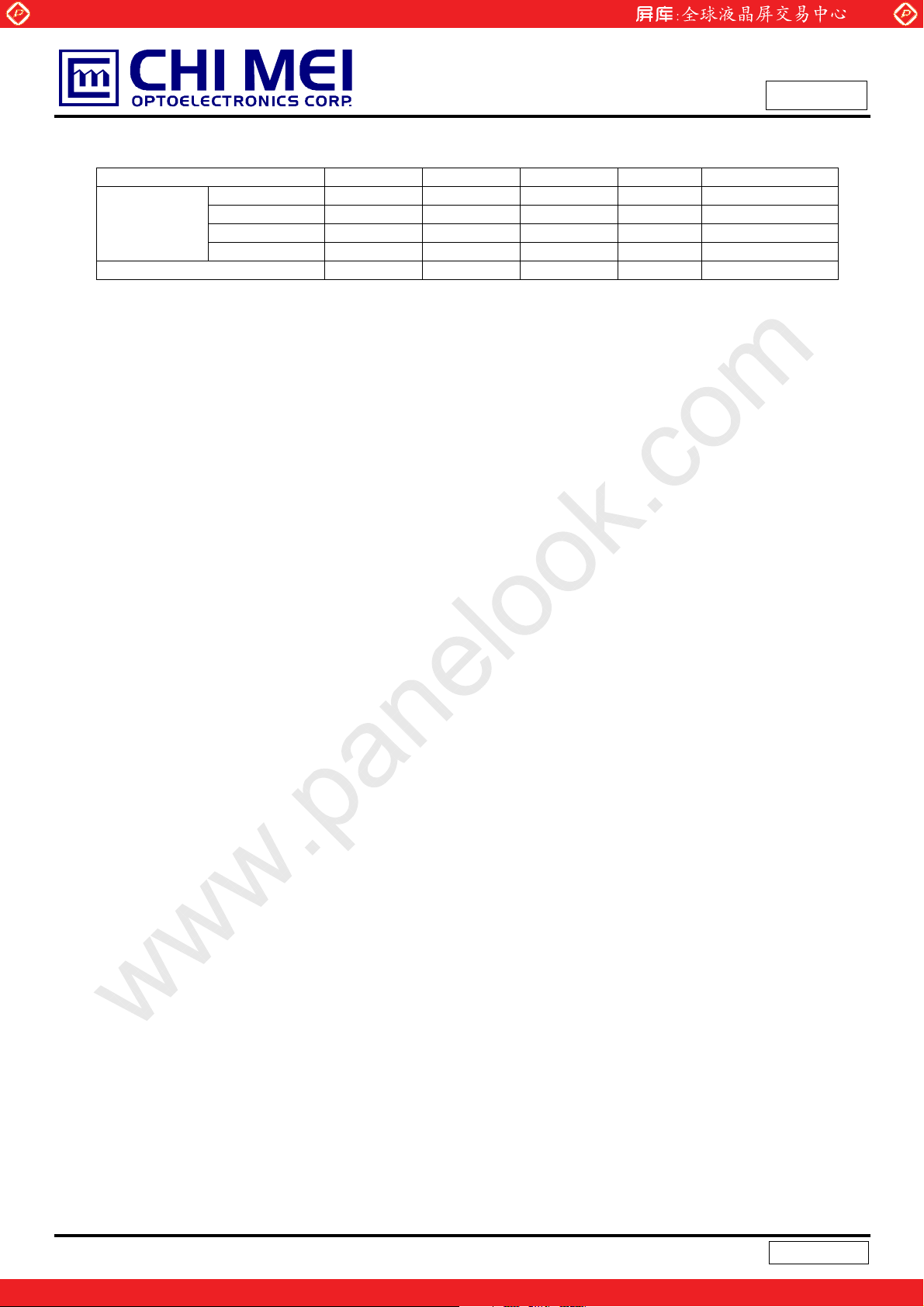
2. ABSOLUTE MAXIMUM RATINGS
2.1 ABSOLUTE RATINGS OF ENVIRONMENT
Item Symbol
Storage Temperature TST -20 +55 ºC (1)
Operating Ambient Temperature TOP 0 45 ºC (1), (2)
Shock (Non-Operating) S
Vibration (Non-Operating) V
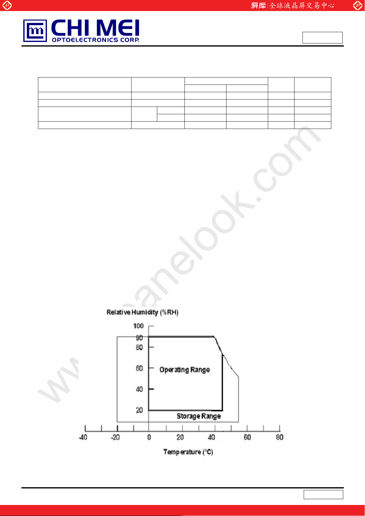
Note (1) Temperature and relative humidity range is shown in the figure below.
(a) 90 %RH Max. (Ta
(b) Wet-bulb temperature should be 39 ºC Max. (Ta > 40 ºC).
(c) No condensation.
Note (2) The maximum operating temperature is based on the test condition that the surface temperature of
display area is less than or equal to 70 ºC with LCD module alone in a temperature controlled chamber.
Thermal management should be considered in your product design to prevent the surface temperature
of display area from being over 70 ºC. The range of operating temperature may degrade in case of
improper thermal management in your product design.
Љ 40 ºC).
Value
Min. Max.
X, Y axis - 30 G (3), (5)
NOP
Z axis - 30 G (3), (5)
- 1.0 G (4), (5)
NOP
Unit Note
Note (3) 11 ms, half sine wave, 1 time for ± X, ± Y, and ± Z.
Note (4) 10 ~ 200 Hz, 10 min, 1 time each X, Y, Z.
Note (5) At testing Vibration and Shock, the fixture in holding the module has to be hard and rigid enough so that
the module would not be twisted or bent by the fixture. The module would not be twisted or bent by the
fixture.
10
6
One step solution for LCD / PDP / OLED panel application: Datasheet, inventory and accessory!
Version 2.2
www.panelook.com
Page 7

Global LCD Panel Exchange Center
www.panelook.com
Issued Date: Sep.25, 2007
Model No.: V562D1-L03
Approval
2.2 RATINGS OF IMAGE STICKING
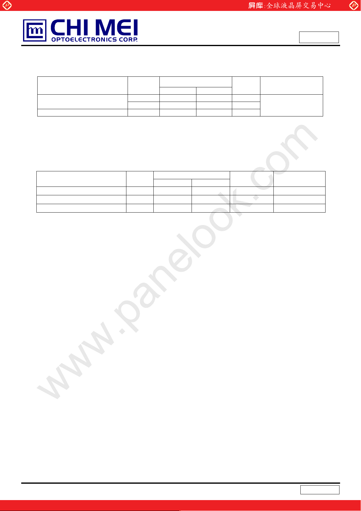
Item Symbol Value Unit Note
Room Temperature Image Sticking RT IS Invisibility 6% ND (%) (1)(3)
High Temperature Image Sticking HT IS Invisibility 6% ND (%) (2)(3)
Note (1) Room temperature image sticking test is at 25
for 12 hours.
Note (2) High temperature image sticking test is at 50
Note (3) Inspection condition is at pattern B (128grade) after 5 mins from pattern A.
A. Pattern A (checker pattern) B. Pattern B (128grade)
3oC environment and fix the pattern A (checker pattern)
3oC environment and fix the pattern A for 12 hours.
7
One step solution for LCD / PDP / OLED panel application: Datasheet, inventory and accessory!
Version 2.2
www.panelook.com
Page 8
Global LCD Panel Exchange Center
3. ELECTRICAL MAXIMUM RATINGS
3.1 TFT LCD MODULE
www.panelook.com
Issued Date: Sep.25, 2007
Model No.: V562D1-L03
Approval
Item Symbol
V
Power Supply Voltage
Logic Input Voltage
Note: (1) Permanent damage to the device may occur if maximum values are exceeded. Function operation
should be restricted to the conditions described under normal operating conditions.
V
CC1
CC2
VIN
Value
Min. Max.
-0.3 20
-0.3 6
-0.3 3.6
Unit Note
V
V
V
(1)
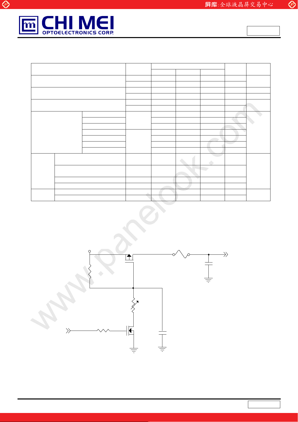
3.2 BACKLIGHT UNIT
Item Symbol
Lamp Voltage VW
Power Supply Voltage VBL 0 30 V
Control Signal Level
Note (1) Permanent damage to the device may occur if maximum values are exceeded. Function operation
should be restricted to the conditions described under Normal Operating Conditions.
Note (2) No moisture condensation or freezing.
Note (3) The control signals include On/Off Control, Internal PWM Control, External PWM Control and
Ё
Val ue
Min. Max.
Ё
-0.3 7 V
5000 V
Unit Note
RMS
(1)
(2), (3)
Internal/External PWM Selection.
8
One step solution for LCD / PDP / OLED panel application: Datasheet, inventory and accessory!
Version 2.2
www.panelook.com
Page 9
Global LCD Panel Exchange Center
4. ELECTRICAL CHARACTERISTICS
4.1 TFT LCD MODULE
Parameter Symbol
Power Supply Voltage
Power Supply Ripple Voltage
Rush Current
White - 1.8 2.4 A
Black - 0.7 - A
Vertical Stripe
Power Supply Current
Differential Input High
LVDS
Interface
Threshold Voltage
Differential Input Low
Threshold Voltage
Common Input Voltage V
Terminating Resistor R
Input High Threshold Voltage VIH 2.7 - 3.3 V CMOS
Interface
Input Low Threshold Voltage V
Note: (1) The module should be always operated within the above ranges.
White - 2.8 - A
Black - 2.3 - A
Vertical Stripe - 2.5 3.2 A
V-Stripe-2column
www.panelook.com
Issued Date: Sep.25, 2007
Model No.: V562D1-L03
Value
Min. Typ. Max.
V
17.1 18 18.9 V
CC1
V
4.5 5 5.5 V
CC2
V
- - 400 mV
RP1
V
200 mV
RP2
I
- - 4.5 A
RUSH1
- - 9.5 A
I
RUSH2
I
CC1
- 1.4 - A
I
CC2
3.4 4.4 A
- - +100 mV
V
LVT H
-100 - mV
V
LVTL
1.125 1.25 1.375 V
LVC
100 ohm
T
0 - 0.7 V
IL
Approval
Unit Note
(1)
(2)
(3)
(2) Measurement conditions:
+5V or +18V
(Low to High)
(Control Signal)
SW
+5.0V or
R1
1K
Q1 Si4485DY
FUSE
VR1
47K
R2
1K
Q2
2N7002
C1
0.01uF
C3
1uF
Vcc 1 or
(LCD Module Input)
9
One step solution for LCD / PDP / OLED panel application: Datasheet, inventory and accessory!
Version 2.2
www.panelook.com
Page 10
Global LCD Panel Exchange Center
GND
www.panelook.com
Vcc rising time is at least 470μs
0.9Vcc
0.1Vcc
470μs
Issued Date: Sep.25, 2007
Model No.: V562D1-L03
Approval
(3)The specified power supply current is under the conditions at Vcc1 = 18 V, Vcc2 = 5 V, Ta = 25 ± 2 ºC,
f
= 60 Hz, whereas a power dissipation check pattern below is displayed.
v
a. White Pattern
c. Vertical Stripe Pattern
b. Black Pattern
Active Area Active Area
R
G
R
B
G
B
B
R
R
G
G
B
B
R
B
R
G
B
R
G
B
R R
G
B
G
B
Active Area
10
One step solution for LCD / PDP / OLED panel application: Datasheet, inventory and accessory!
R
Version 2.2
www.panelook.com
Page 11
Global LCD Panel Exchange Center
4.2 BACKLIGHT UNIT
www.panelook.com
Issued Date: Sep.25, 2007
Model No.: V562D1-L03
Approval
4.2.1 CCFL (Cold Cathode Fluorescent Lamp) CHARACTERISTICS (Ta=25
Parameter Symbol
Lamp Voltage VW
Min. Typ. Max.
- 1728 -
Lamp Current IL 5.5 6.0 6.5 mA
- - 2550
Lamp Starting Voltage VS
- - 2350
Value
2кккк
)
Unit Note
V
I
RMS
RMS
(2), Ta = 0 ºC
V
RMS
(2), Ta = 25 ºC
V
RMS
=5.7mA
L
(1)
Operating Frequency Fo 40 60 80 KHz (3)
Lamp Life Time LBL - 50000 - Hrs (4)
4.2.2 INVERTER CHARACTERISTICS (Ta=25
Parameter Symbol
Power Consumption
P
- 315 330 W (5), IL = 6.0mA
BL
Power Supply Voltage VBL 22.8 24.0 25.2 VDC
Power Supply Current IBL - 13.13 13.75 A Non Dimming
Input Ripple Noise - - - 500 mV
Oscillating Frequency FW 47 50 53 kHz
Dimming frequency FB 150 160 180 Hz
Minimum Duty Ratio D
- 20 - %
MIN
Note (1) Lamp current is measured by utilizing high frequency current meters as shown below:
Min. Typ. Max.
2кккк
)
Val ue
Unit Note
VBL=22.8V
P-P
Note (2) The lamp starting voltage V
should be applied to the lamp for more than 1 second after startup.
S
Otherwise the lamp may not be turned on.
Note (3) The lamp frequency may produce interference with horizontal synchronous frequency of the
display input signals, and it may result in line flow on the display. In order to avoid interference, the
lamp frequency should be detached from the horizontal synchronous frequency and its harmonics
as far as possible.
Note (4) The life time of a lamp is defined as when the brightness is larger than 50% of its original value and
the effective discharge length is longer than 80% of its original length (Effective discharge length is
defined as an area that has equal to or more than 70% brightness compared to the brightness at
the center point of lamp.) as the time in which it continues to operate under the condition at Ta = 25
2к and I
Note (5) The power supply capacity should be higher than the total inverter power consumption P
= 5.5 ~ 6.5mA rms.
L
. Since
BL
the pulse width modulation (PWM) mode was applied for backlight dimming, the driving current
changed as PWM duty on and off. The transient response of power supply should be considered
for the changing loading when inverter dimming.
Note (6) The measurement condition of Max. value is based on 56" backlight unit under input voltage 24V
, average lamp current 6.3 mA and lighting 30 minutes later.
11
One step solution for LCD / PDP / OLED panel application: Datasheet, inventory and accessory!
Version 2.2
www.panelook.com
Page 12
Global LCD Panel Exchange Center
www.panelook.com
Issued Date: Sep.25, 2007
Model No.: V562D1-L03
Approval
Inverter
(Master)
a
1
2
a
a
1
2
a
a
1
2
a
a
1
2
a
a
1
2
a
a
1
2
a
a
1
2
a
a
1
2
a
HV (White -)
HV(Blue -)
HV (White +)
HV(Blue +)
HV (White -)
HV(Blue -)
HV (White +)
HV(Blue +)
HV (White -)
HV(Blue -)
HV (White +)
HV(Blue +)
HV (White -)
HV(Blue -)
HV (White +)
HV(Blue +)
A
A
A
A
A
A
A
A
A
A
A
A
A
A
A
A
HV (Pink +)
HV (White +)
HV (Pink -)
HV (White -)
HV (Pink +)
HV (White +)
HV (Pink -)
HV (White -)
HV (Pink +)
HV (White +)
HV (Pink -)
HV (White -)
HV (Pink +)
HV (White +)
HV (Pink -)
HV (White -)
A
b
1
2
A
b
1
A
b
2
A
b
1
A
b
2
A
b
A
b
1
2
A
b
A
b
1
A
b
2
A
b
1
A
b
2
1
A
b
2
A
b
A
b
1
2
A
b
Inverter
(Slave 2)
Inverter
(Slave 1)
LCD Module
a
1
2
a
1
a
2
a
1
a
2
a
a
1
2
a
a
1
2
a
a
1
2
a
a
1
2
a
1
a
2
a
HV (White -)
HV(Blue -)
HV (White +)
HV(Blue +)
HV (White -)
HV(Blue -)
HV (White +)
HV(Blue +)
HV (White -)
HV(Blue -)
HV (White +)
HV(Blue +)
HV (White -)
HV(Blue -)
HV (White +)
HV(Blue +)
A
A
A
A
A
A
A
A
A
A
A
A
A
A
A
A
HV (Pink +)
HV (White +)
HV (Pink -)
HV (White -)
HV (Pink +)
HV (White +)
HV (Pink -)
HV (White -)
HV (Pink +)
HV (White +)
HV (Pink -)
HV (White -)
HV (Pink +)
HV (White +)
HV (Pink -)
HV (White -)
A
b
1
A
b
2
A
b
1
2
A
b
A
b
1
2
A
b
A
b
1
A
b
2
A
b
1
A
b
2
A
b
1
A
b
2
A
b
1
A
b
2
A
b
1
2
A
b
Inverter
(Slave 3)
12
One step solution for LCD / PDP / OLED panel application: Datasheet, inventory and accessory!
Version 2.2
www.panelook.com
Page 13
Global LCD Panel Exchange Center
4.2.3 INVERTER INTERTFACE CHARACTERISTICS
Parameter Symbol
On/Off Control Voltage
Internal/External PWM
Select Voltage
Voltage
Voltage
VBL Rising Time Tr1 웎 30 웎 50 ms
VBL Falling Time Tf1 웎 30 웎 50 ms
Control Signal Rising Time Tr
Control Signal Falling Time Tf
PWM Signal Rising Time T
PWM Signal Falling Time T
Input impedance RIN
PWM Delay Time T
BLON Delay Time Ton Ё 300 Ё 500 ms
BLON Off Time T
ON
OFF
HI
LO
MAX 3.15 3.3 3.45 V Note (5) Internal PWM Control
MIN
HI 2.0
LO
www.panelook.com
Issued Date: Sep.25, 2007
Model No.: V562D1-L03
Ё
0
0
0
1
Val ue
Ё
Ё
Ё-
Ё
0
Ё
Ё
5.0 V
0.8 V
5.0 V
0.8 V
Ё
5.0 V duty onExternal PWM Control
0.8 V duty off
100 ms
100 ms
50 us
50 us
Ё Ё MӨ
Unit Note
Vminimum duty ratio
Te st
Condition
V
BLON
V
SEL
V
V
IPWM
V
V
EPWM
PW MR
PW MF
Ё 100 300 mS
PW M
Ё 300 Ё 500 ms
off
Ё
Ё
Ё
Ё
= L
SEL
= H
SEL
Ё Ё Ё
Ё Ё Ё
Ё Ё Ё
Ё Ё Ё
Ё
Min. Typ. Max.
2.0
2.0
Approval
Note (1) The SEL signal should be valid before backlight turns on by BLON signal. It is inhibited to change
the internal/external PWM selection (SEL) during backlight turn on period.
Note (2) The power sequence and control signal timing are shown in the following figure.
Note (3) The power sequence and control signal timing must follow the figure below. For a certain reason,
the inverter has a possibility to be damaged with wrong power sequence and control signal timing.
Note (4) Abnormal operation may occur if these maximum values of control signal are exceeded.
Note (5) The range of V
the start dimming point) except the Max. value of V
for dimming brightness should be constrained from 0V to 2.85V (i.e., 2.85V is
IPWM
mentioned here is only for the maximum
IPWM
brightness useful. In other words, 2.85V~3.15V is not suggested for using to prevent from possibly
abnormal phenomenon.
13
One step solution for LCD / PDP / OLED panel application: Datasheet, inventory and accessory!
Version 2.2
www.panelook.com
Page 14

Global LCD Panel Exchange Center
www.panelook.com
Issued Date: Sep.25, 2007
Model No.: V562D1-L03
Approval
V
V
V
BL
V
BLON
V
SEL
EPWM
IPWM
Tr1
2.0V
0.8V
2.0V
0.8V
2.0V
0.8V
3.0V
Ton
Backlight on duration
Tr
Ext. Dimming Function
T
PWMR
PWM
T
T
Tf
Int. Dimming Function
PWMF
0
0
0
0
0
Tf1
Toff
V
W
External
PWM
Period
External
PWM Duty
100%
Minimun
Duty
14
One step solution for LCD / PDP / OLED panel application: Datasheet, inventory and accessory!
Version 2.2
www.panelook.com
Page 15

Global LCD Panel Exchange Center
(
)
5. BLOCK DIAGRAM
5.1 TFT LCD MODULE
2B_Odd_Data0(+/-)
2B_Odd_Data1(+/-)
2B_Odd_Data2(+/-)
2B_Odd_Data3(+/-)
2B_Odd_Clock(+/-)
2B_Even_Data0(+/-)
2B_Even_Data1(+/-)
2B_Even_Data2(+/-)
2B_Even_Data3(+/-)
2B_Even_Clock(+/-)
1B_Odd_Data0(+/-)
1B_Odd_Data1(+/-)
1B_Odd_Data2(+/-)
1B_Odd_Data3(+/-)
1B_Odd_Clock(+/-)
1B_Even_Data0(+/-)
1B_Even_Data1(+/-)
1B_Even_Data2(+/-)
1B_Even_Data3(+/-)
1B_Even_Clock(+/-)
2A_Odd_Data0(+/-)
2A_Odd_Data1(+/-)
2A_Odd_Data2(+/-)
2A_Odd_Data3(+/-)
2A_Odd_Clock(+/-)
2A_Even_Data0(+/-)
2A_Even_Data1(+/-)
2A_Even_Data2(+/-)
2A_Even_Data3(+/-)
2A_Even_Clock(+/-)
1A_Odd_Data0(+/-)
1A_Odd_Data1(+/-)
1A_Odd_Data2(+/-)
1A_Odd_Data3(+/-)
1A_Odd_Clock(+/-)
1A_Even_Data0(+/-)
1A_Even_Data1(+/-)
1A_Even_Data2(+/-)
1A_Even_Data3(+/-)
1A_Even_Clock(+/-)
CN9.
Vcc1
Vcc2
GND
B-C,FX15-41S-0.
5SH
Hirose
CN13
CN14
B-F,FI-RE51S-HF,
JAE Taiwan.
POWER
CONNECTOR
(S20B-PHDS
S-B(LF)(SN))
www.panelook.com
Issued Date: Sep.25, 2007
Model No.: V562D1-L03
Approval
CONNECTOR
INPUT
FRAME
BUFFER
TIMING
CONTROLLER
CONNECTOR
INPUT
DC/DC CONVERTER
& REFERENCE
VOLTAGE
GENERATOR
SCAN DRIVER
DATA DRIVER (RSDS)
TFT LCD PANEL
(3840x3x2160)
DATA DRIVER (RSDS)
SCAN DRIVER
VBL
GND
SEL
E_PWM
I_PWM
BLON
INVERTER
CONNECTOR
CN1:S14B-PH-SM4-TB
(D)(LF) or equivalent
(Master)
CN8-CN23:SM02 (12.0)B-BHS-1-TB(LF)(JST)
VBL
GND
CN4,CN6: 528521070 (Molex)
INVERTER
CONNECTOR
CN2:S12B-PH-SM4-TB
(D)(LF) or equivalent
(Slave)
CN3,CN5: 528521070 (Molex)
or equivalent
BACKLIGHT
UNIT
INVERTER
CONNECTOR
CN2:S12B-PH-SM4-TB
(D)(LF) or equivalent
(Slave)
INVERTER
CONNECTOR
CN2:S12B-PH-SM4-TB
(D)(LF) or equivalent
(Slave)
VBL
GND
VBL
GND
CN5,CN7: 528521070 (Molex)
15
One step solution for LCD / PDP / OLED panel application: Datasheet, inventory and accessory!
Version 2.2
www.panelook.com
Page 16

Global LCD Panel Exchange Center
www.panelook.com
6. LCD INPUT TERMINAL PIN ASSIGNMENT
6.1 TFT LCD MODULE L.V.D.S. INPUT
CN13 Connector Pin Assignment
Pin No. Name Description Note
1 2B_ORX3+ Positive transmission data of Odd pixel 3.
2 2B_ORX3- Negative transmission data of Odd pixel 3.
3 2B_ OCLK + Positive of Odd clock.
4 2B_ OCLK- Negative of Odd clock.
5 2B_ORX2+ Positive transmission data of Odd pixel 2.
6 2B_ORX2- Negative transmission data of Odd pixel 2.
7 2B_ORX1+ Positive transmission data of Odd pixel 1.
Issued Date: Sep.25, 2007
Model No.: V562D1-L03
Approval
8 2B_ORX1- Negative transmission data of Odd pixel 1.
9 2B_ORX0+ Positive transmission data of Odd pixel 0.
10 2B_ORX0- Negative transmission data of Odd pixel 0.
11 2B_ERX0- Negative transmission data of Even pixel 0.
12 2B_ERX0+ Positive transmission data of Even pixel 0.
13 2B_ERX1- Negative transmission data of Even pixel 1.
14 2B_ERX1+ Positive transmission data of Even pixel 1.
15 2B_ERX2- Negative transmission data of Even pixel 2.
16 2B_ERX2+ Positive transmission data of Even pixel 2.
17 2B_ ECLK- Negative of Even clock.
18 2B_ ECLK+ Positive of Even clock.
19 2B_ERX3- Negative transmission data of Even pixel 3.
20 2B_ERX3+ Positive transmission data of Even pixel 3.
21 GND Ground.
22 2A_ORX0- Negative transmission data of Odd pixel 0.
23 2A_ORX0+ Positive transmission data of Odd pixel 0.
24 2A_ORX1- Negative transmission data of Odd pixel 1.
25 2A_ORX1+ Positive transmission data of Odd pixel 1.
26 2A_ORX2- Negative transmission data of Odd pixel 2.
27 2A_ORX2+ Positive transmission data of Odd pixel 2.
28 2A_ OCLK- Negative of Odd clock.
29 2A_ OCLK+ Positive of Odd clock.
30 2A_ORX3- Negative transmission data of Odd pixel 3.
31 2A_ORX3+ Positive transmission data of Odd pixel 3.
32 2A_ERX3+ Positive transmission data of Even pixel 3.
16
One step solution for LCD / PDP / OLED panel application: Datasheet, inventory and accessory!
Version 2.2
www.panelook.com
Page 17

Global LCD Panel Exchange Center
33 2A_ERX3- Negative transmission data of Even pixel 3.
34 2A_ ECLK+ Positive of Even clock.
35 2A_ ECLK- Negative of Even clock.
36 2A_ERX2+ Positive transmission data of Even pixel 2.
37 2A_ERX2- Negative transmission data of Even pixel 2.
38 2A_ERX1+ Positive transmission data of Even pixel 1.
39 2A_ERX1- Negative transmission data of Even pixel 1.
40 2A_ERX0+ Positive transmission data of Even pixel 0.
41 2A_ERX0- Negative transmission data of Even pixel 0.
CN14 Connector Pin Assignment
www.panelook.com
Issued Date: Sep.25, 2007
Model No.: V562D1-L03
Approval
Pin No. Name Description Note
1 NC Not connect
2 NC Not connect
3
4 NC Not connect
5 NC Not connect
6 NC Not connect
7 NC Not connect
8 NC Not connect
9 GND Ground.
10 1B_ORX3+ Positive transmission data of Odd pixel 3.
11 1B_ORX3- Negative transmission data of Odd pixel 3.
12 1B_ OCLK + Positive of Odd clock.
13 1B_ OCLK- Negative of Odd clock.
14 1B_ORX2+ Positive transmission data of Odd pixel 2.
15 1B_ORX2- Negative transmission data of Odd pixel 2.
ODSEL Overdrive Lookup Table Selection
(3)
16 1B_ORX1+ Positive transmission data of Odd pixel 1.
17 1B_ORX1- Negative transmission data of Odd pixel 1.
18 1B_ORX0+ Positive transmission data of Odd pixel 0.
19 1B_ORX0- Negative transmission data of Odd pixel 0.
20 1B_ERX0- Negative transmission data of Even pixel 0.
21 1B_ERX0+ Positive transmission data of Even pixel 0.
22 1B_ERX1- Negative transmission data of Even pixel 1.
23 1B_ERX1+ Positive transmission data of Even pixel 1.
24 1B_ERX2- Negative transmission data of Even pixel 2.
17
One step solution for LCD / PDP / OLED panel application: Datasheet, inventory and accessory!
Version 2.2
www.panelook.com
Page 18

Global LCD Panel Exchange Center
25 1B_ERX2+ Positive transmission data of Even pixel 2.
26 1B_ ECLK- Negative of Even clock.
27 1B_ ECLK+ Positive of Even clock.
28 1B_ERX3- Negative transmission data of Even pixel 3.
29 1B_ERX3+ Positive transmission data of Even pixel 3.
30 GND Ground.
31 1A_ORX0- Negative transmission data of Odd pixel 0.
32 1A_ORX0+ Positive transmission data of Odd pixel 0.
33 1A_ORX1- Negative transmission data of Odd pixel 1.
34 1A_ORX1+ Positive transmission data of Odd pixel 1.
35 1A_ORX2- Negative transmission data of Odd pixel 2.
www.panelook.com
Issued Date: Sep.25, 2007
Model No.: V562D1-L03
Approval
36 1A_ORX2+ Positive transmission data of Odd pixel 2.
37 1A_ OCLK- Negative of Odd clock.
38 1A_ OCLK+ Positive of Odd clock.
39 1A_ORX3- Negative transmission data of Odd pixel 3.
40 1A_ORX3+ Positive transmission data of Odd pixel 3.
41 1A_ERX3+ Positive transmission data of Even pixel 3.
42 1A_ERX3- Negative transmission data of Even pixel 3.
43 1A_ ECLK+ Positive of Even clock.
44 1A_ ECLK- Negative of Even clock.
45 1A_ERX2+ Positive transmission data of Even pixel 2.
46 1A_ERX2- Negative transmission data of Even pixel 2.
47 1A_ERX1+ Positive transmission data of Even pixel 1.
48 1A_ERX1- Negative transmission data of Even pixel 1.
49 1A_ERX0+ Positive transmission data of Even pixel 0.
50 1A_ERX0- Negative transmission data of Even pixel 0.
51 GND Ground.
Note: (1) CN13 connector part no.: B-C,FX15-41S-0.5SH,Hirose electric.
(2) CN14 connector part no.: B-F,FI-RE51S-HF,JAE Taiwan.
(3)
ODSEL
in accordance to the frame rate to optimize image quality.
(Overdrive Lookup Table Selection). The overdrive lookup table should be selected
ODSEL Note
L Lookup table was optimized for 60Hz frame rate.
H Lookup table was optimized for 50Hz frame rate.
(4) “L” and “H” operation in (3) could follow “CMOS Interface” in Section 4.1
18
One step solution for LCD / PDP / OLED panel application: Datasheet, inventory and accessory!
Version 2.2
www.panelook.com
Page 19

Global LCD Panel Exchange Center
y
y
y
y
y
y
y
y
6.2 TFT LCD MODULE POWER INPUT
CN9 Connector Pin Assignment
Pin No. S
1 VIN +18.0V power suppl
2 VIN +18.0V power suppl
3 V5VC +5.0V power suppl
4 V5VC +5.0V power suppl
5 V5VC +5.0V power suppl
6 NC Not connection
7 V5VC +5.0V power suppl
8 NC Not connection
9 V5VC +5.0V power suppl
10 NC Not connection
11 GND Ground
12 NC Not connection
13 GND Ground
14 NC Not connection
15 GND Ground
16 NC Not connection
17 GND Ground
18 GND Ground
19 GND Ground
20 GND Ground
mbol Description Note
www.panelook.com
Issued Date: Sep.25, 2007
Model No.: V562D1-L03
Approval
(1)
Note: (1) CN9 connector part no.: S20B-PHDSS-B(LF)(SN), JST(
ֲءᚘထጤ),ᐚຏጤ or equivalent.
19
One step solution for LCD / PDP / OLED panel application: Datasheet, inventory and accessory!
Version 2.2
www.panelook.com
Page 20

Global LCD Panel Exchange Center
www.panelook.com
Issued Date: Sep.25, 2007
Model No.: V562D1-L03
Approval
6.3 BACKLIGHT UNIT
The pin configuration for the housing and the leader wire is shown in the table below.
Pin Name Description Wire Color
1 HV High Voltage Pink
2 HV High Voltage White
Note (1) The backlight interface housing for high voltage side is a model BHR-04VS-1, manufactured by
JST and the mating header on inverter part number is SM02 (12.0) B-BHS-1-TB (LF).
1 HV(White)
2 HV(Pink)
CN8-CN23: BHR-04VS-1 (JST).
1 HV(White)
2 HV(Pink)
1 HV(White)
2 HV(Pink)
1 HV(Pink)
2
HV(White)
1
HV(Pink)
2 HV(White)
1 HV(Pink)
2 HV(White)
1
1
Ϥ
Ϥ
2
2
Ϥ
Ϥ
≈
31
Ϥ
32
Ϥ
20
One step solution for LCD / PDP / OLED panel application: Datasheet, inventory and accessory!
Version 2.2
www.panelook.com
Page 21

Global LCD Panel Exchange Center
6.4 INVERTER UNIT
CN1 (Master, Header): S14B-PH-SM4-TB (D)(LF)(JST) or equivalent
Pin No. Symbol Description
1
2
3
4
5
6
7
8
9
10
11
12 E_PWM
13 I_PWM
14 BLON Backlight on/off control
VBL +24V
GND GND
Internal/external PWM selection
SEL
High : external dimming
Low : internal dimming
External PWM control signal
E_PWM should be connected to ground when internal PWM was selected
(SEL = Low).
Internal PWM Control Signal
I_PWM should be connected to ground when external PWM was selected
(SEL = High).
power input
DC
www.panelook.com
Issued Date: Sep.25, 2007
Model No.: V562D1-L03
Approval
CN2 (Slave, Header): S12B-PH-SM4-TB (D)(LF)(JST) or equivalent
Pin No. Symbol Description
1
2
3
4
5
6
7
8
9
10
11
12 NC NC
CN8-CN15 (Master, Header), CN16-CN23 (Slave, Header): SM02 (12.0) B-BHS-1-TB (LF)(JST) or equivalent
Pin No. Symbol Description
1
2
VBL +24V
GND GND
NC NC
CCFL HOT
CCFL HOT
CCFL high voltage
CCFL high voltage
power input
DC
21
One step solution for LCD / PDP / OLED panel application: Datasheet, inventory and accessory!
Version 2.2
www.panelook.com
Page 22

Global LCD Panel Exchange Center
CN3-CN4 (Master, Header), CN5-CN7 (Slave, Header): 528521070 (Molex)
Pin No. Symbol Description
1 Board to Board
2
3
4
5
6
7
8
9
10
Note (1) Floating of any control signal is not allowed.
Control
Signal
Board to Board
Board to Board
Board to Board
Board to Board
Board to Board
Board to Board
Board to Board
Board to Board
Board to Board
www.panelook.com
Issued Date: Sep.25, 2007
Model No.: V562D1-L03
Approval
22
One step solution for LCD / PDP / OLED panel application: Datasheet, inventory and accessory!
Version 2.2
www.panelook.com
Page 23

Global LCD Panel Exchange Center
6.5 BLOCK DIAGRAM OF IMAGE SIGNAL
The video picture (3840x2160) should be divided into four parts: each one is 960x2160 resolution. Signals of
these four parts should be delivered into the module individually through each 2-channel LVDS interface. But it
must be “synchronous” mutually between signals from these four 2-channel LVDS interfaces. And the protocol is
specified in the LVDS interface specification.
www.panelook.com
Issued Date: Sep.25, 2007
Model No.: V562D1-L03
Approval
2CH 2CH
2CH 2CH
23
One step solution for LCD / PDP / OLED panel application: Datasheet, inventory and accessory!
Version 2.2
www.panelook.com
Page 24

Global LCD Panel Exchange Center
p
OR0
www.panelook.com
6.6 BLOCK DIAGRAM OF NORMAL L.V.D.S.
CN13, CN14
Issued Date: Sep.25, 2007
Model No.: V562D1-L03
Approval
ERx0+
ER0-ER7
-
-
ERx1+
ERx1-
ERx2+
OR0-OR7
-
-
ERx3+
ERx3-
ECLK+
Host
Graphics
Controller
ORx0+
ORx1+
ORx1-
51
Ө
51
51
51
51
51
51
51
100pF
Ө
Ө
100pF
Ө
Ө
100pF
Ө
Ө
100pF
Ө
-
-
RxOUT
ER0-ER7
-
-
-OR7
-
-
51
Ө
51
100pF
Ө
-
Timing
51
Ө
51
51
100pF
Ө
Ө
100
F
-
Controller
Standard Reference::
LVDS Transmitter
THC63LVDM83A
(LVDF83A)
ORx2+
-
ORx3+
ORx3-
OCLK+
24
51
Ө
100pF
51
Ө
51
Ө
100pF
51
Ө
51
Ө
51
100pF
Ө
-
LVDS Receiver in CMO Side
Version 2.2
One step solution for LCD / PDP / OLED panel application: Datasheet, inventory and accessory!
www.panelook.com
Page 25

Global LCD Panel Exchange Center
ER0~ER7 : Even pixel R data
EG0~EG7 : Even pixel G data
EB0~EB7 : Even pixel B data
OR0~OR7 : Odd pixel R data
OG0~OG7: Odd pixel G data
OB0~OB7 : Odd pixel B data
DE : Data enable signal
DCLK : Data clock signal
Notes: (1) The driving system must have the transmitter to drive the module.
(2) LVDS cable impedance shall be 50 ohms per signal line or about 100 ohms per twist-pair line
when it is used differentially.
www.panelook.com
Issued Date: Sep.25, 2007
Model No.: V562D1-L03
Approval
(3) Two pixel data are sent into the module for every clock cycle. The first pixel of the frame is even
pixel and the second pixel is odd pixel.
25
One step solution for LCD / PDP / OLED panel application: Datasheet, inventory and accessory!
Version 2.2
www.panelook.com
Page 26

Global LCD Panel Exchange Center
6.7 L.V.D.S. INTERFACE DEFINITION
SIGNAL
TRANSMITTER
THC63LVDM83A
PIN INPUT Host TFT-LCD PIN OUTPUT
www.panelook.com
INTERFACE CONNECTOR
Issued Date: Sep.25, 2007
RECEIVER
THC63LVDF84A
Model No.: V562D1-L03
Approval
TFT CONTROL
INPUT
24bit
R0
R1
R2
R3
R4
R5
G0
G1
G2
G3
G4
G5
B0
B1
B2
B3
B4
B5
DE
R6
R7
G6
G7
B6
B7
RSVD 1
RSVD 2
RSVD 3
DCLK 31 TxCLK IN
51
52
54
55
56
3
4
6
7
11
12
14
15
19
20
22
23
24
30
50
2
8
10
16
18
25
27
28
TxIN0
TxIN1
TxIN2
TxIN3
TxIN4
TxIN6
TxIN7
TxIN8
TxIN9
TxIN12
TxIN13
TxIN14
TxIN15
TxIN18
TxIN19
TxIN20
TxIN21
TxIN22
TxIN26
TxIN27
TxIN5
TxIN10
TxIN11
TxIN16
TxIN17
TxIN23
TxIN24
TxIN25
TA OUT0+
TA OUT0-
TA OUT1+
TA OUT1-
TA OUT2+
TA OUT2-
TA OUT3+
TA OUT3-
TxCLK OUT+
TxCLK OUT-
Rx 0+
Rx 0-
Rx 1+
Rx 1-
Rx 2+
Rx 2-
Rx 3+
Rx 3-
RxCLK IN+
RxCLK IN-
27
29
30
32
33
35
37
38
39
43
45
46
47
51
53
54
55
1
6
7
34
41
42
49
50
2
3
5
26 RxCLK OUT DCLK
Rx OUT0
Rx OUT1
Rx OUT2
Rx OUT3
Rx OUT4
Rx OUT6
Rx OUT7
Rx OUT8
Rx OUT9
Rx OUT12
Rx OUT13
Rx OUT14
Rx OUT15
Rx OUT18
Rx OUT19
Rx OUT20
Rx OUT21
Rx OUT22
Rx OUT26
Rx OUT27
Rx OUT5
Rx OUT10
Rx OUT11
Rx OUT16
Rx OUT17
Rx OUT23
Rx OUT24
Rx OUT25
R0
R1
R2
R3
R4
R5
G0
G1
G2
G3
G4
G5
B0
B1
B2
B3
B4
B5
DE
R6
R7
G6
G7
B6
B7
Not connect
Not connect
Not connect
R0~R7: Pixel R Data (7; MSB, 0; LSB)
G0~G7: Pixel G Data (7; MSB, 0; LSB)
B0~B7: Pixel B Data (7; MSB, 0; LSB)
DE : Data enable signal
DCLK : Data clock signal
Notes (1) RSVD(reserved)pins on the transmitter shall be “H” or “L”.
26
One step solution for LCD / PDP / OLED panel application: Datasheet, inventory and accessory!
Version 2.2
www.panelook.com
Page 27

Global LCD Panel Exchange Center
6.8 COLOR DATA INPUT ASSIGNMENT
The brightness of each primary color (red, green and blue) is based on the 8-bit gray scale data input for the
color. The higher the binary input the brighter the color. The table below provides the assignment of color
versus data input. Note (1) 0: Low Level Voltage, 1: High Level Voltage
Color
R7 R6 R5 R4 R3 R2 R1 R0 G7 G6 G5 G4 G3 G2 G1 G0 B7 B6 B5 B4 B3 B2 B1 B0
Basic
Colors
Gray
Scale
Of
Red
Black
Red
Green
Blue
Cyan
Magenta
Yellow
White
Red(0) / Dark
Red(1)
Red(2)
:
:
Red(253)
Red(254)
Red(255)
0
0
0
1
1
1
0
0
0
0
0
0
0
0
0
1
1
1
1
1
1
1
1
1
0
0
0
0
0
0
0
0
0
:
:
:
:
:
:
1
1
1
1
1
1
1
1
1
www.panelook.com
Issued Date: Sep.25, 2007
Model No.: V562D1-L03
Approval
Data Signal
Red Green Blue
0
0
0
0
0
0
0
0
0
0
0
0
0
0
0
0
0
0
0
0
0
1
1
1
1
1
0
0
0
0
0
0
0
0
0
0
0
0
0
0
0
0
0
0
0
0
0
1
1
1
1
1
1
1
1
0
0
0
0
0
0
0
0
0
0
0
0
0
0
0
0
0
0
0
0
0
1
1
1
1
1
1
1
1
0
0
0
0
0
1
1
1
1
1
1
1
1
1
1
1
1
1
1
1
1
1
1
1
1
1
0
0
0
0
0
0
0
0
1
1
1
1
1
1
1
1
1
1
1
1
1
1
1
1
1
1
1
1
1
0
0
0
0
0
0
0
0
1
1
1
1
1
1
1
1
1
1
1
1
1
1
1
1
1
1
1
1
1
0
0
0
0
0
0
0
0
0
0
0
0
0
0
0
0
0
0
0
0
0
0
0
0
1
0
0
0
0
0
0
0
0
0
0
0
0
0
0
1
0
0
0
0
0
0
0
0
0
0
0
0
:
:
:
:
:
:
:
:
:
:
:
:
:
:
:
:
:
:
:
:
:
:
:
:
:
:
:
:
:
:
1
1
1
0
1
0
0
0
0
0
0
0
0
0
1
1
1
1
0
0
0
0
0
0
0
0
0
0
1
1
1
1
1
0
0
0
0
0
0
0
0
0
:
:
0
0
0
0
0
0
0
0
0
:
:
:
:
0
0
0
0
0
0
0
0
0
0
0
0
0
0
:
:
:
:
:
:
0
0
0
0
0
0
0
0
0
Gray
Scale
Of
Green
Gray
Scale
Of
Blue
Green(0)/Dark
Green(1)
Green(2)
:
:
Green(253)
Green(254)
Green(255)
Blue(0) / Dark
Blue(1)
Blue(2)
:
:
Blue(253)
Blue(254)
Blue(255)
0
0
0
0
0
0
0
0
0
0
0
0
0
0
0
0
0
0
0
0
0
0
0
0
0
0
0
0
0
0
0
0
0
1
0
0
0
0
0
0
0
0
0
0
0
0
0
0
0
0
1
0
0
0
:
:
:
:
:
:
:
:
:
:
:
:
:
:
:
:
:
:
:
:
:
:
:
:
:
:
:
:
:
:
:
:
:
:
:
:
0
0
0
0
0
0
0
0
1
1
1
1
1
1
0
1
0
0
0
0
0
0
0
0
0
0
1
1
1
1
1
1
1
0
0
0
0
0
0
0
0
0
0
0
1
1
1
1
1
1
1
1
0
0
0
0
0
0
0
0
0
0
0
0
0
0
0
0
0
0
0
0
0
0
0
0
0
0
0
0
0
0
0
0
0
0
0
0
0
0
0
0
0
0
0
0
0
0
0
0
0
0
0
0
0
0
0
0
:
:
:
:
:
:
:
:
:
:
:
:
:
:
:
:
:
:
:
:
:
:
:
:
:
:
:
:
:
:
:
:
:
:
:
:
0
0
0
0
0
0
0
0
0
0
0
0
0
0
0
0
1
1
0
0
0
0
0
0
0
0
0
0
0
0
0
0
0
0
1
1
0
0
0
0
0
0
0
0
0
0
0
0
0
0
0
0
1
1
0
0
0
0
0
0
0
0
0
0
:
:
:
:
0
0
0
0
0
0
0
0
0
0
0
0
:
:
:
:
1
1
1
1
1
1
0
0
0
:
:
:
:
0
0
0
0
0
0
0
0
0
0
0
0
:
:
:
:
1
1
1
1
1
1
0
0
0
0
0
:
:
:
:
0
0
0
0
0
0
0
0
0
1
1
0
:
:
:
:
0
1
0
1
1
1
27
One step solution for LCD / PDP / OLED panel application: Datasheet, inventory and accessory!
Version 2.2
www.panelook.com
Page 28

Global LCD Panel Exchange Center
g
(4)
(2)
(3)
y
k
y
k
www.panelook.com
7. TIMING REQUIREMENTS OF IMAGE SIGNAL
7.1 INPUT SIGNAL TIMING SPECIFICATIONS
The input signal timing specifications are shown as the following table and timing diagram.
Si
nal Item Symbol Min. Typ. Max. Unit Note
LVDS Receiver Clock
(1-CH LVDS)
LVDS Receiver Data
Vertical Active Display Term
(2-CH LVDS,960x 2160 Active Area)
Horizontal Active Display Term
(2-CH LVDS,960x 2160 Active Area)
Note: (1) Since this module is operated in DE only mode, Hsync and Vsync input signals should be set to
Frequency 1/Tc 60 72 72 MH
Input cycle to
cycle jitter
Setup Time
Hold Time
Frame Rate
Total Tv 2164 2164 2300 Th Tv=Tvd+Tvb
Displa
Blan
Total Th 1100 1100 1175 Tc Th=Thd+Thb
Displa
Blan
Issued Date: Sep.25, 2007
Model No.: V562D1-L03
Z
Trcl - - 200 ps
Tlvsu 600 - - ps
Tlvhd 600 - - ps
Fr
5
6
Fr
Tvd - 2160 - Th
Tvb 4 4 140 Th
Thd - 960 - Tc
Thb 140 140 215 Tc
47 50 53 Hz
57 60 63 Hz
Approval
low logic level. Otherwise, this module would operate abnormally.
(2) (ODSEL) = (H). Please refer to Section 6.1 for detail information.
(3) (ODSEL) = (L). Please refer to Section 6.1 for detail information.
(4) The value of Typ. is based on 60Hz operation.
INPUT SIGNAL TIMING DIAGRAM
Tvd
DE
T
h
Tv
Tvb
Д
DCLK
DE
DATA
Д
T
hb
Thd
Valid display data (480 DCLK)
28
One step solution for LCD / PDP / OLED panel application: Datasheet, inventory and accessory!
Д
Д
Version 2.2
www.panelook.com
Page 29

Global LCD Panel Exchange Center
www.panelook.com
Issued Date: Sep.25, 2007
Model No.: V562D1-L03
Approval
RXCLK+/-
RXn+/-
Tlvsu
Tlvhd
1T
14
LVDS RECEIVER TIMING DIAGRAM
Tc
3T
14
5T
14
7T
14
9T
14
11T
14
13T
14
29
One step solution for LCD / PDP / OLED panel application: Datasheet, inventory and accessory!
Version 2.2
www.panelook.com
Page 30

Global LCD Panel Exchange Center
7.2 POWER ON/OFF SEQUENCE
To prevent a latch-up or DC operation of LCD module, the power on/off sequence should be
www.panelook.com
Issued Date: Sep.25, 2007
Model No.: V562D1-L03
Approval
followed as the diagram below.
ˣ˸ʳ˦˿
ˣ˸ʳ˦˿
ˣ˸ʳ˦˿ˣ˸ʳ˦˿
˩˶˶˄ʿʳ˩˶˶˅
˃ˁˈЉ˧˄Љ˄˃ʻ˩˶˶˄ʼ
˃ˁˈЉ˧ˊЉ˄˃ʻ˩˶˶˅ʼ
˃Љ˧ˋЉˈ˃
˃Љ˧˅Љˈ˃
˃Љ˧ˆЉˈ˃
ˈ˃˃Љ˧ˇ
˦˼˺˴˿
˦˼˺˴˿
˦˼˺˴˿˦˼˺˴˿
˕˴˶˾˿˼˺˻ʳʻ˥˸˶˸˷˸˷ʼ
ˈ˃˃Љ˧ˈ
˄˃˃Љ˧ˉ
˃˩
˃˩
˃˩
˃ˁˌ˩˶˶ ˄
˃ˁ˄˩˶˶ ˄
˧˄
˧˄
˃ˁˌ˩˶˶ ˅
˧˄˧˄
˃ˁ˄˩˶˶ ˅
˧ˊ
˧ˊ
˧ˊ˧ˊ
˧ˋ
˧ˋ
˧ˋ˧ˋ
˧˅
˧˅
˧˅˧˅
˩˔˟˜˗
ˣ˸ʳˢ ˣ˸ʳˢ˹˹
ˈ˃ʸ ˈ˃ʸ
˧ˈ
˧ˈ ˧ˉ
˧ˈ˧ˈ
˃ˁˌ˩˶˶ ˅
˧ˉ
˧ˉ˧ˉ
˃ˁˌ˩˶˶ ˄
˃ˁ˄˩˶˶ ˄
˃ˁ˄˩˶˶˅
˧ˆ
˧ˆ
˧ˆ˧ˆ
˧ˇ
˧ˇ
˧ˇ˧ˇ
ˣ˸ʳˢˡ˂ˢ˙˙ʳ˦˸˸˶˸
ˣ˸ʳˢˡ˂ˢ˙˙ʳ˦˸˸˶˸
ˣ˸ʳˢˡ˂ˢ˙˙ʳ˦˸˸˶˸ˣ˸ʳˢˡ˂ˢ˙˙ʳ˦˸˸˶˸
Note : (1) The supplied voltage of the external system for the module input should follow the definition of Vcc1,2.
(2) Apply the lamp voltage within the LCD operation range. When the backlight turns on before the LCD
operation or the LCD turns off before the backlight turns off, the display may momentarily become
abnormal screen.
(3) In case of Vcc1,2 is in off level, please keep the level of input signals on the low and avoid floating.
(4) T4 should be measured after the module being fully discharged between power off and on period.
(5) Interface signal shall not be kept at high impedance when the power is on.
30
One step solution for LCD / PDP / OLED panel application: Datasheet, inventory and accessory!
Version 2.2
www.panelook.com
Page 31

Global LCD Panel Exchange Center
8. OPTICAL CHARACTERISTICS
8.1 TEST CONDITIONS
Item Symbol Value Unit
Ambient Temperature Ta
Ambient Humidity Ha
Supply Voltage VCC 5.0 V
Input Signal According to typical value in "3. ELECTRICAL CHARACTERISTICS"
Lamp Current IL
Oscillating Frequency (Inverter) FL
Frame Rate Fr 60 Hz
8.2 OPTICAL SPECIFICATIONS
The relative measurement methods of optical characteristics are shown in 8.2 Notes. The following items
www.panelook.com
25±2
50±10
6.0±0.5
50±3
Issued Date: Sep.25, 2007
Model No.: V562D1-L03
Approval
o
C
%RH
mA
KHz
should be measured under the test conditions described in 8.1 and stable environment shown in Note (6).
Item Symbol Condition Min. Typ. Max. Unit Note
Contrast Ratio CR 900 1200 - Note (2)
Response Time
Center Luminance of White L
Average Luminance of White
White Variation
Cross Talk CT 2 % Note (5)
Red
Green
Color
Chromaticity
Blue
White
Gray to
gray
C
L
400 450 - cd/m2Note (4)
AVE
δW
=0°, θY =0°
θ
x
Rx 0.651 -
Ry
Gx
Gy
Bx
By
Wx
Wy
Viewing angle at
normal direction
6.5 ms Note (3)
400 450 cd/m2Note (4)
1.6 - Note (7)
Typ.
-0.03
0.332
0.269
0.593
0.144
0.060
0.285
0.293
Typ.
+0.03
-
-
Note (6)
-
-
-
-
72 75 % NTSC
80 88
80 88
80 88
80 88
Viewing
Angle
Color Gamut C.G
Horizontal
Vertical
θx+
θ
-
x
θY+
θ
Y
-
CR≥30
31
One step solution for LCD / PDP / OLED panel application: Datasheet, inventory and accessory!
Deg. Note (1)
Version 2.2
www.panelook.com
Page 32

Global LCD Panel Exchange Center
Note (1) Definition of Viewing Angle (θx, θy):
Viewing angles are measured by Eldim EZ-Contrast 160R
www.panelook.com
Issued Date: Sep.25, 2007
Model No.: V562D1-L03
Approval
Note (2) Definition of Contrast Ratio (CR):
θX- = 90º
6 o’clock
θ
y-
= 90º
The contrast ratio can be calculated by the following expression.
Contrast Ratio (CR) = L255 / L0
L255: Luminance of gray level 255
x-
y-
Normal
θx = θy = 0º
θy- θy+
θx−
θx+
y+
12 o’clock direction
θ
y+
= 90º
x+
θX+ = 90º
L 0: Luminance of gray level 0
CR = CR (7), where CR (X) is corresponding to the Contrast Ratio of the point X at the figure in Note
(7).
Note (3) Definition of Gray to Gray Switching Time:
The driving signal means the signal of gray level 0, 63, 127, 191, 255.
Gray to gray average time means the average switching time of gray level 0 ,63,127,191,255 to each
100%
90%
Optical
Response
10%
0%
Gray to gray
switching time
Time
Time
Gray to gray
switching time
other.
32
One step solution for LCD / PDP / OLED panel application: Datasheet, inventory and accessory!
Version 2.2
www.panelook.com
Page 33

Global LCD Panel Exchange Center
(
)
(
)
Note (4) Definition of Luminance of White (LC, L
Measure the luminance of gray level 255 at center point and 5 points
LC = L (7)
L
= [L (4)+ L (5)+ L (7)+ L (9)+ L (10)] / 5
AVE
Where L (x) is corresponding to the luminance of the point X at the figure in Note (7).
Note (5) Definition of Cross Talk (CT):
www.panelook.com
):
AVE
Issued Date: Sep.25, 2007
Model No.: V562D1-L03
Approval
CT = | Y
– YA | / YA × 100 (%)
B
Where:
Y
= Luminance of measured location without gray level 255 pattern (cd/m2)
A
Y
= Luminance of measured location with gray level 255 pattern (cd/m2)
B
(0, 0)
Y
(D/8,W/2)
A, L
Y
(D/2,7W/8)
A, D
Active Area
Gray 128
Y
Y
D,W
A, U
A, R
(D/2,W /8)
(7D/8,W/2)
(D/4,W/4)
Y
(D/8,W/2)
B, L
Y
(D/2,7W/8)
B, D
0, 0
Active Area
Gray 0
Gray 255
Gray 128
Y
B, U
Y
B, R
(3D/4,3W/4)
(D,W)
(D/2,W /8)
(7D/8,W/2)
33
One step solution for LCD / PDP / OLED panel application: Datasheet, inventory and accessory!
Version 2.2
www.panelook.com
Page 34

Global LCD Panel Exchange Center
Note (6) Measurement Setup:
The LCD module should be stabilized at given temperature for 1 hour to avoid abrupt
temperature change during measuring. In order to stabilize the luminance, the measurement
should be executed after lighting backlight for 1 hour in a windless room.
LCD Module
www.panelook.com
Issued Date: Sep.25, 2007
Model No.: V562D1-L03
Approval
LCD Panel
Center of the Screen
Note (7) Definition of White Variation (δW):
Measure the luminance of gray level 128 at 13 points
δW = Maximum [L (1), L (2), L (3), L (4),
Display Color Analyzer
(Minolta CA210)
Light Shield Room
(Ambient Luminance < 2 lux)
ΕΕΕ, L (13)] / Minimum [L (1), L (2), L (3), L (4),ΕΕΕ , L (13)]
D
D/10 9D/10
3D/10 5D/10 7D/10
W/10
1
2
3
10
5
: Test Point
8
13
X
X=1 to 13
4
7
W
3W /10
5W /10
6
Vertical Line
7W /10
9W /10
11
9
12
Active Area
34
Version 2.2
One step solution for LCD / PDP / OLED panel application: Datasheet, inventory and accessory!
www.panelook.com
Page 35

Global LCD Panel Exchange Center
www.panelook.com
Issued Date: Sep.25, 2007
Model No.: V562D1-L03
Approval
9. PRECAUTIONS
9.1 ASSEMBLY AND HANDLING PRECAUTIONS
(1) Do not apply rough force such as bending or twisting to the module during assembly.
(2) It is recommended to assemble or to install a module into the user’s system in clean working areas. The
dust and oil may cause electrical short or worsen the polarizer.
(3) Do not apply pressure or impulse to the module to prevent the damage of LCD panel and Backlight.
(4) Always follow the correct power-on sequence when the LCD module is turned on. This can prevent the
damage and latch-up of the CMOS LSI chips.
(5) Do not plug in or pull out the I/F connector while the module is in operation.
(6) Do not disassemble the module.
(7) Use a soft dry cloth without chemicals for cleaning, because the surface of polarizer is very soft and
easily scratched.
(8) Moisture can easily penetrate into LCD module and may cause the damage during operation.
(9) When storing modules as spares for a long time, the following precaution is necessary.
a. Do not leave the module in high temperature, and high humidity for a long time.It is highly
recommended to store the module with temperature from 0 to 35кat normal humidity
without condensation.
b. The module shall be stored in dark place. Do not store the TFT-LCD module in direct
sunlight or fluorescent light.
(10) When ambient temperature is lower than 10ºC, the display quality might be reduced. For example, the
response time will become slow, and the starting voltage of CCFL will be higher than that of room
temperature.
9.2 SAFETY PRECAUTIONS
(1) The startup voltage of a Backlight is approximately 1000 Volts. It may cause an electrical shock while
assembling with the inverter. Do not disassemble the module or insert anything into the Backlight unit.
(2) If the liquid crystal material leaks from the panel, it should be kept away from the eyes or mouth. In case
of contact with hands, skin or clothes, it has to be washed away thoroughly with soap.
(3) After the module’s end of life, it is not harmful in case of normal operation and storage.
9.3 SAFETY STANDARDS
The LCD module should be certified with safety regulations as follows:
(1) UL60950-1 or updated standard.
(2) IEC60950-1 or updated standard.
(3) UL60065 or updated standard.
(4) IEC60065 or updated standard.
35
One step solution for LCD / PDP / OLED panel application: Datasheet, inventory and accessory!
Version 2.2
www.panelook.com
Page 36

Global LCD Panel Exchange Center
10.DEFINITION OF LABELS
10.1 CMO MODULE LABEL
The barcode nameplate is pasted on each module as illustration, and its definitions are as following explanation.
www.panelook.com
Issued Date: Sep.25, 2007
Model No.: V562D1-L03
Approval
V562D1 -L03 Rev. XX
CHI MEI
OPTOELECTRONICS
X X X X X X X Y M D L N N N N
(a) Model Name: V562D1-L03
(b) Revision: Rev. XX, for example: A0, A1… B1, B2… or C1, C2…etc.
(c) Serial ID: X X
X X X X X Y M D L N N N N
Serial No.
Product Line
Year, Month, Date
CMO Internal Use
CMO Internal Use
Revision
E207943
MADE IN TAIWAN
RoHS
Serial ID includes the information as below:
(a) Manufactured Date: Year: 0~9, for 2000~2009
Month: 1~9, A~C, for Jan. ~ Dec.
Day: 1~9, A~Y, for 1
(b) Revision Code: Cover all the change
(c) Serial No.: Manufacturing sequence of product
(d) Product Line: 1 -> Line1, 2 -> Line 2, …etc.
CMO Internal Use
st
to 31st, exclude I ,O, and U.
36
One step solution for LCD / PDP / OLED panel application: Datasheet, inventory and accessory!
Version 2.2
www.panelook.com
Page 37

Global LCD Panel Exchange Center
11. PACKAGE
11.1 PACKING SPECIFICATIONS
(1) 2 LCD TV modules / 1 Box
(2) Box dimensions : 1448(L) X 372 (W) X 901 (H)
(3) Weight : approximately 56Kg (2 modules per box)
(4) One protective film is attached on the LCD TV
11.2 PACKING METHOD
Figures 9-1 and 9-2 are the packing method
LCD TV Module
www.panelook.com
Issued Date: Sep.25, 2007
Model No.: V562D1-L03
Approval
4pcs Drier
Cushion(Bottom)
Anti-static Bag
Carton
Carton Label
4pcs Joint
Figure.9-1 packing method
37
One step solution for LCD / PDP / OLED panel application: Datasheet, inventory and accessory!
Version 2.2
www.panelook.com
Page 38

Global LCD Panel Exchange Center
Sea Transportation
Corner Protector:L1780*50mm*50mm
Corner Protector:L1130*50mm*50mm
Pallet:L1150*W1460*H140mm
Pallet Stack:L1150*W1460*H1942mm
Gross:353kg
www.panelook.com
Issued Date: Sep.25, 2007
Model No.: V562D1-L03
Approval
PP Belt
PP Belt
Figure. 9-2 Packing method
38
One step solution for LCD / PDP / OLED panel application: Datasheet, inventory and accessory!
Version 2.2
www.panelook.com
Page 39

Global LCD Panel Exchange Center
12. MECHANICAL CHARACTERISTIC
www.panelook.com
Issued Date: Sep.25, 2007
Model No.: V562D1-L03
Approval
ڻႝηިҽԖϦљ
CHI MEI
39
One step solution for LCD / PDP / OLED panel application: Datasheet, inventory and accessory!
Version 2.2
www.panelook.com
Page 40

Global LCD Panel Exchange Center
www.panelook.com
Issued Date: Sep.25, 2007
Model No.: V562D1-L03
Approval
ڻႝηިҽԖϦљ
CHI MEI
40
One step solution for LCD / PDP / OLED panel application: Datasheet, inventory and accessory!
Version 2.2
www.panelook.com
Page 41

Global LCD Panel Exchange Center
www.panelook.com
Issued Date: Sep.25, 2007
Model No.: V562D1-L03
Approval
ڻႝηިҽԖϦљ
CHI MEI
41
One step solution for LCD / PDP / OLED panel application: Datasheet, inventory and accessory!
Version 2.2
www.panelook.com
Page 42

Global LCD Panel Exchange Center
www.panelook.com
Issued Date: Sep.25, 2007
Model No.: V562D1-L03
Approval
ڻႝηިҽԖϦљ
CHI MEI
42
One step solution for LCD / PDP / OLED panel application: Datasheet, inventory and accessory!
Version 2.2
www.panelook.com
 Loading...