

Page 1
Global LCD Panel Exchange Center
TFT LCD Approval Specification
(Specifically for Mitsubishi)
MODEL NO.: V562D1 - L02
www.panelook.com
Issued Date: Sep. 1, 2008
Model No.: V562D1-L02
Approval
Customer: Mitsubishi
Approved by:
Note:
Approved By
TV Head Division
LY Ch en
One step solution for LCD / PDP / OLED panel application: Datasheet, inventory and accessory!
Reviewed By
LCD TV Marketing and Product Management Div.
Prepared By
QRA Dept. Product Development Div.
Tomy Chen WT Lin
Henry Teng
1
Version2.5
www.panelook.com
Page 2

Global LCD Panel Exchange Center
www.panelook.com
Issued Date: Sep. 1, 2008
Model No.: V562D1-L02
Approval
- CONTENTS -
REVISION HISTORY ------------------------------------------------------- 3
1. GENERAL DESCRIPTION ------------------------------------------------------- 5
1.1 OVERVIEW
1.2 FEATURES
1.3 APPLICATION
1.4 GENERAL SPECIFICATI0NS
1.5 MECHANICAL SPECIFICATIONS
2. ABSOLUTE MAXIMUM RATING ------------------------------------------------------- 7
2.1 ABSOLUTE RATINGS OF ENVIRONMENT
2.2 RATINGS OF IMAGE STICKING
3. ELECTRICAL MAXIMUM RATINGS ------------------------------------------------------- 9
3.1 TFT LCD MODULE
3.2 BACKLIGHT UNIT
4. ELECTRICAL CHARACTERISTICS ------------------------------------------------------- 10
4.1 TFT LCD MODULE
4.2 BACKLIGHT UNIT
4.2.1 CCFL CHARACTERISTICS
4.2.2 INVERTER CHARACTERISTICS
4.2.3 INVERTER INTERTFACE CHARACTERISTIC
5. BLOCK DIAGRAM ------------------------------------------------------- 17
5.1 TFT LCD MODULE
6. LCD INPUT TERMINAL PIN ASSIGNMENT ------------------------------------------------------- 18
6.1 TFT LCD MODULE DVI INPUT
6.2 TFT LCD MODULE POWER INPUT
6.3 BACKLIGHT UNIT
6.4 INVERTER UNIT
6.5 BLOCK DIAGRAM OF IMAGE SIGNAL
6.6 DVI SIGNAL LIST
6.7 DVI LINK TIMING REQUIREMENTS
7. INTERFACE TIMING ------------------------------------------------------- 25
7.1 INPUT SIGNAL TIMING SPECIFICATIONS
7.2 EXTENDED DISPLAY IDENTIFICATION DADA (EDID)
7.3 EXTENDED DISPLAY IDENTIFICATION DADA (EDID) CODE
7.4 POWER ON/OFF SEQUENCE
8. OPTICAL CHARACTERISTICS ------------------------------------------------------- 29
8.1 TEST CONDITIONS
8.2 OPTICAL SPECIFICATIONS
9. PRECAUTIONS
9.1 ASSEMBLY AND HANDLING PRECAUTIONS
9.2 SAFETY PRECAUTIONS
9.3 SAFETY STANDARDS
10. DEFINITION OF LABELS
10.1 CMO MODULE LABEL
-------------------------------------------------------
-------------------------------------------------------
33
34
2
One step solution for LCD / PDP / OLED panel application: Datasheet, inventory and accessory!
Version2.5
www.panelook.com
Page 3
Global LCD Panel Exchange Center
y
www.panelook.com
11. PACKAGE
11.1 PACKING SPECIFICATIONS
11.2 PACKING METHOD
-------------------------------------------------------
12. MECHANICAL CHARACTERISTICS
-------------------------------------------------------
Appendix 1 (CMO Guarantee List)
Appendix 2 (Service Parts Revision Description)
------------------------------------------------------
------------------------------------------------------
Appendix 3 (Part No./Revision/Modification Record of Parts)
Reference1 (Modification Record of CC Board)
Reference2 (Modification Record of Inverter)
------------------------------------------------------
------------------------------------------------------
Reference3 (Modification Record of Screw Number on BLU Frame)
Reference4 (Modification Record of Pin Supporter)
Reference5 (
Externals Drawing of
Service Parts)
Picture 1
------------------------------------------------------
------------------------------------------------------
-----------------------------------------------------
Version Date
REVISION HISTORY
Page
Section Description
(New)
Issued Date: Sep. 1, 2008
Model No.: V562D1-L02
Approval
----------------------------------------
-------------------------------
35
37
41
41
42
43
44
45
46
47
52
Ver 2.0
Ver 2.1
Mar. 9,’07
Jun. 22,’07
All
6
15
17
20
41
41
42
43
44
45
46
47
52
4.2.3
-
-
-
All
1.5
5.1
6.4
-
-
-
-
-
-
Approval Specification is first issued.
Modify the value of Horizontal(H) and Vertical(V).
Note (4) EPWM dut
100%.
Modify CN1:S14B-PH-SM4-TB(D)(LF).
Modify CN2:S12B-PH-SM4-TB(D)(LF).
Modify CN1:S14B-PH-SM4-TB(D)(LF).
Modify CN2:S12B-PH-SM4-TB(D)(LF).
Add Appendix 1
Add Appendix 2
Add Appendix 3
Add Reference 1
Add Reference 2
Add Reference 3
Add Reference 4
Add Reference 5
Add Picture 1
ratio without inverter shut down is 0~95 % and
3
One step solution for LCD / PDP / OLED panel application: Datasheet, inventory and accessory!
Version2.5
www.panelook.com
Page 4
Global LCD Panel Exchange Center
p
www.panelook.com
Issued Date: Sep. 1, 2008
Model No.: V562D1-L02
Approval
Ver 2.2
Ver 2.3
Ver 2.4
Ver 2.5
Aug. 13,’07
Sep. 25,’07
Feb. 12,’08
Sep. 1,’08
12
12
13
13
29
42
44
41
42
44
42
38
39
42
4.2.1
4.2.2
4.2.2
4.2.2
8.1
Appendix 3
Reference 2
Appendix 2
Appendix 3
Reference 2
Appendix 3
12
12
Appendix 3
Modify the value of Lamp Current.
Modify the value of Power Consumption and Power Supply Current.
Modify Note (4) I
Modify Note (6) average lamp current 6.3mA.
Modify the value of Lamp Current.
Add C2 Revision.
Add modification record of “CP point rework for 6.0mA lam
current”.
Modify inverter revision to Rev.2E (Rev.9).
Add record of “C2 After 10/5”.
Add modification record of “Rev.2E”.
Add record of C3.
Modify mechanical diagram to represent adding sensor holes.
Modify mechanical diagram to represent adding sensor holes.
Add record of “C4”.
= 5.5 ~ 6.5mA rms.
L
4
One step solution for LCD / PDP / OLED panel application: Datasheet, inventory and accessory!
Version2.5
www.panelook.com
Page 5
Global LCD Panel Exchange Center
1. GENERAL DESCRIPTION
1.1 OVERVIEW
V562D1-L02 is a 56” Thin-Film-Transistor Liquid-Crystal (TFT-LCD) module with one 32-CCFL backlight unit
and 4 ports Single-DVI utilization. This module supports 3840 x 2160 Quad Full High Definition (QFHD) TV
format and can display 16.7M colors (8-bit). The inverter module for backlight is also built-in.
1.2 FEATURES
- Ultra Wide Viewing Angle (176(H)/ 176(V) for CR>30)
- High Brightness (500 nits)
- High Contrast Ratio (1200:1)
- Ultra Fast Response Time (Gray to gray average 6.5 ms)
- High Color Saturation (NTSC 75%)
- QFHD (3840 x 2160 pixels) Resolution
- 4 Ports Single-DVI (Digital Visual Interface)
- RoHS Compliance
www.panelook.com
Issued Date: Sep. 1, 2008
Model No.: V562D1-L02
Approval
1.3 APPLICATION
- Luxurious Living Room TVs
- Public Display
- Home Theater
- Satellite Communication
- Medical Analyses/ Instruction
- Security and Monitoring
- Industrial Design
- 3D Display
- Digital Museum
- Multi-Media Display
1.4 GENERAL SPECIFICATI0NS
Item Specification Unit Note
Active Area 1244.16 (H) x 699.84 (V) (56.2” diagonal) mm
Bezel Opening Area 1252.1 (H) x 707.8 (V) mm
Driver Element a-si TFT active matrix - Pixel Number 3840x R.G.B. x 2160 pixel Pixel Pitch(Sub Pixel) 0.108 (H) x 0.324 (V) mm Pixel Arrangement RGB vertical stripe - Display Colors 16.7M color Display Operation Mode Transmissive mode / Normally black - -
Surface Treatment
Note (1) The specifications of the surface treatment are temporarily for this phase. CMO reserves the rights
Low reflection coating< 2% reflection
Hard coating 3H
- (1)
to change this feature.
5
One step solution for LCD / PDP / OLED panel application: Datasheet, inventory and accessory!
Version2.5
www.panelook.com
Page 6
Global LCD Panel Exchange Center
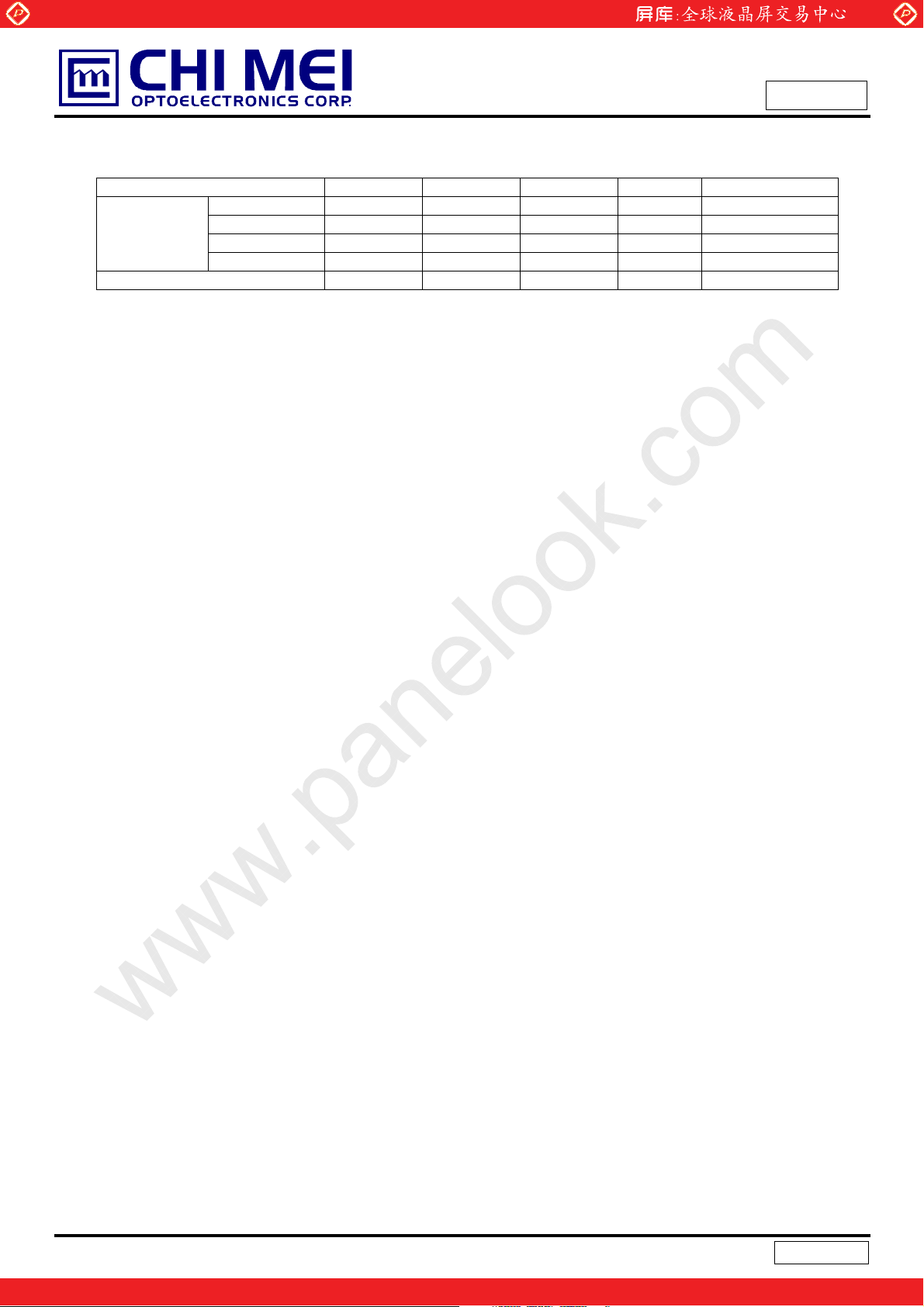
1.5 MECHANICAL SPECIFICATIONS
Item Min. Typ. Max. Unit Note
Horizontal(H)
Module Size
Vertical(V)
Depth(D)
Depth(D)
Weight
www.panelook.com
1309 1309.5 1310.2
766.5 767 767.7
57.2 58.5 59.8
61.9 63.2 64.5
23000 23500 24000
Issued Date: Sep. 1, 2008
Model No.: V562D1-L02
Approval
mm
mm
mm To PCB cover
mm To inverter cover
g
6
One step solution for LCD / PDP / OLED panel application: Datasheet, inventory and accessory!
Version2.5
www.panelook.com
Page 7
Global LCD Panel Exchange Center
2. ABSOLUTE MAXIMUM RATING
www.panelook.com
Issued Date: Sep. 1, 2008
Model No.: V562D1-L02
Approval
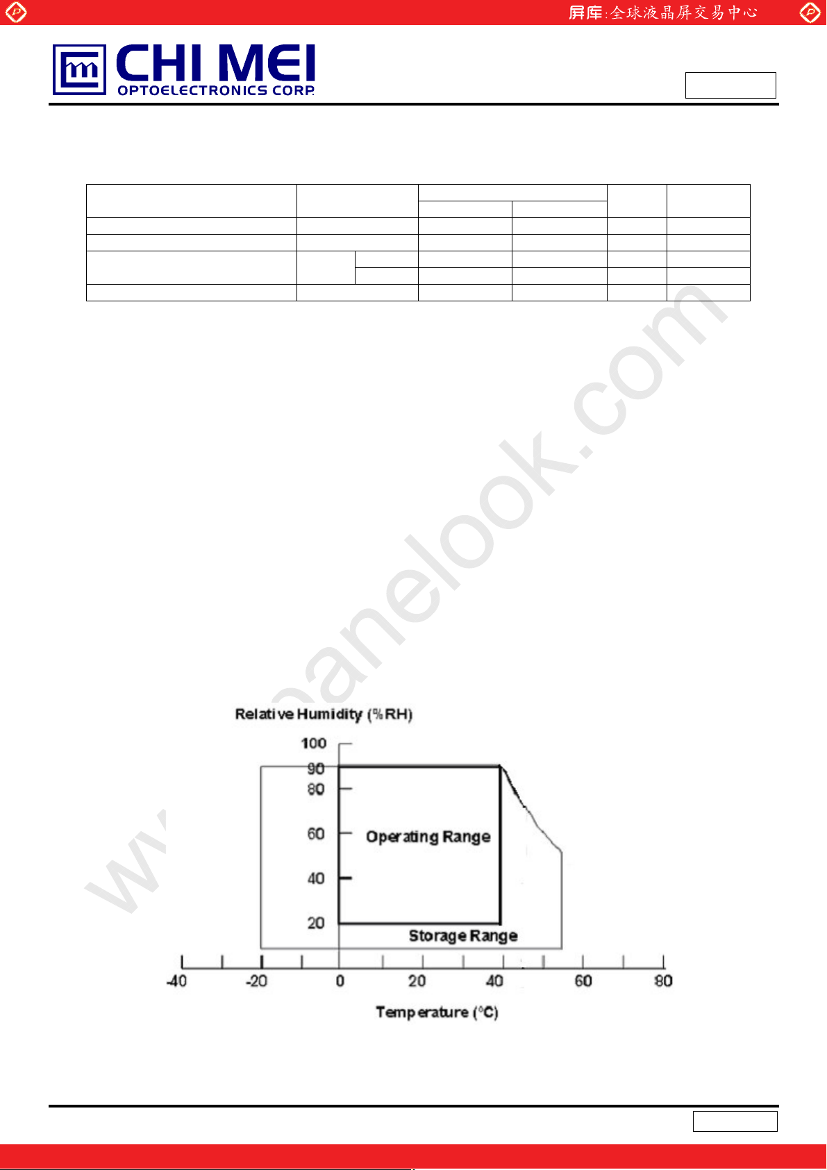
2.1 ABSOLUTE RATINGS OF ENVIRONMENT
Item Symbol
Storage Temperature TST -20 +55 ºC (1)
Operating Ambient Temperature TOP 0 40 ºC (1), (2)
Shock (Non-Operating) S
Vibration (Non-Operating) V
Note (1) Temperature and relative humidity range is shown in the figure below.
(a) 90 %RH Max. (Ta
(b) Wet-bulb temperature should be 39 ºC Max. (Ta > 40 ºC).
(c) No condensation.
Note (2) The maximum operating temperature is based on the test condition that the surface temperature of
display area is less than or equal to 65 ºC with LCD module alone in a temperature controlled chamber.
Thermal management should be considered in your product design to prevent the surface temperature
of display area from being over 65 ºC. The range of operating temperature may degrade in case of
improper thermal management in your product design.
Note (3) 11 ms, half sine wave, 1 time for ± X, ± Y, and ± Z.
Љ
40 ºC).
NOP
Value
Min. Max.
X, Y axis - 30 G (3), (5)
Z axis - 30 G (3), (5)
- 1.0 G (4), (5)
NOP
Unit Note
Note (4) 10 ~ 200 Hz, 10 min, 1 time each X, Y, Z.
Note (5) At testing Vibration and Shock, the fixture in holding the module has to be hard and rigid enough so that
the module would not be twisted or bent by the fixture. The module would not be twisted or bent by the
fixture.
10
7
One step solution for LCD / PDP / OLED panel application: Datasheet, inventory and accessory!
Version2.5
www.panelook.com
Page 8

Global LCD Panel Exchange Center
www.panelook.com
Issued Date: Sep. 1, 2008
Model No.: V562D1-L02
Approval
2.2 RATINGS OF IMAGE STICKING
Item Symbol Value Unit Note
Room Temperature Image Sticking RT IS Invisibility 6% ND (%) (1)(3)
High Temperature Image Sticking HT IS Invisibility 6% ND (%) (2)(3)
Note (1) Room temperature image sticking test is at 25
for 12 hours.
Note (2) High temperature image sticking test is at 50
Note (3) Inspection condition is at pattern B (128grade) after 5 mins from pattern A.
3oC environment and fix the pattern A (checker pattern)
3oC environment and fix the pattern A for 12 hours.
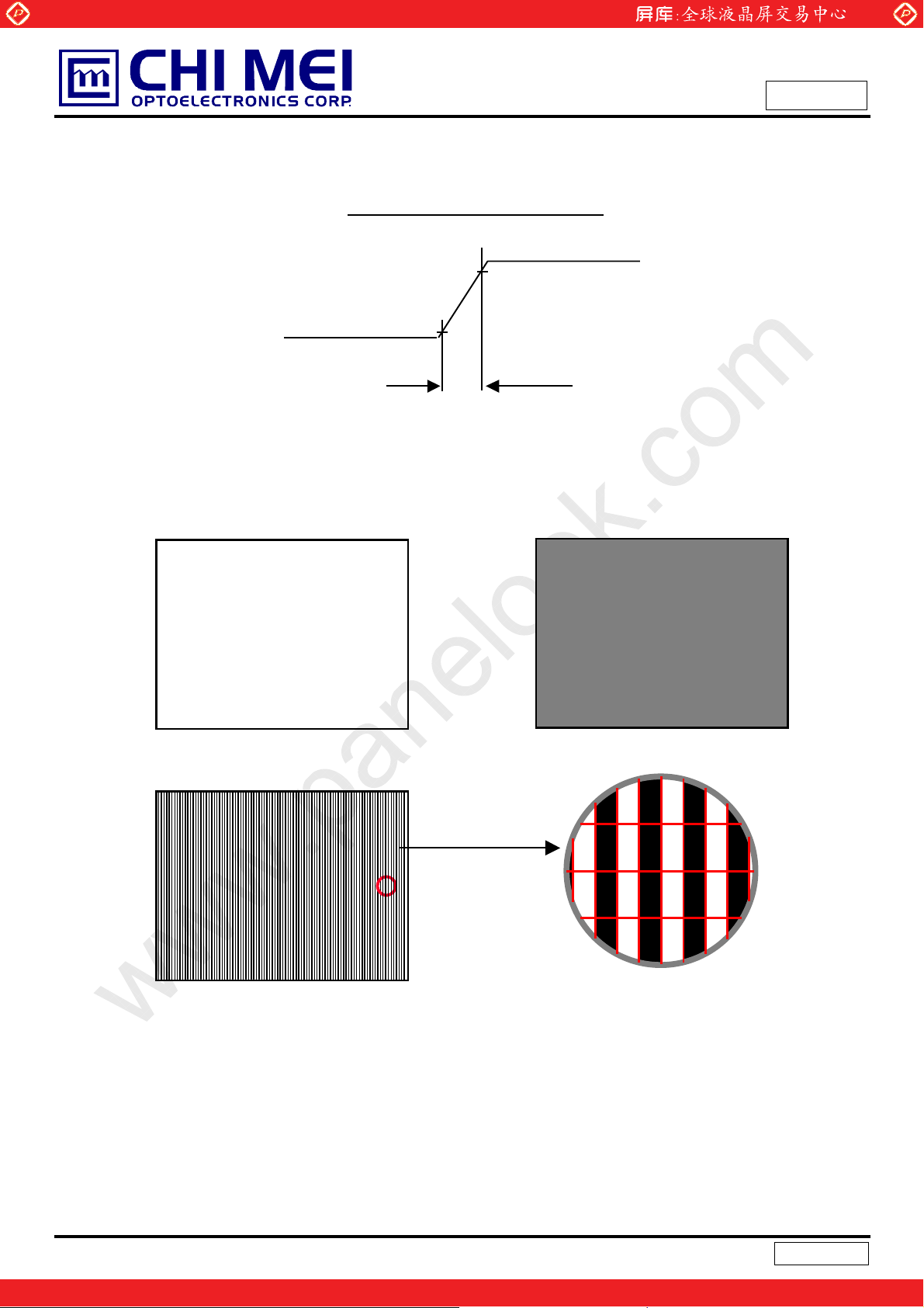
A. Pattern A (checker pattern) B. Pattern B (128grade)
8
One step solution for LCD / PDP / OLED panel application: Datasheet, inventory and accessory!
Version2.5
www.panelook.com
Page 9
Global LCD Panel Exchange Center
3. ELECTRICAL MAXIMUM RATINGS
3.1 TFT LCD MODULE
www.panelook.com
Issued Date: Sep. 1, 2008
Model No.: V562D1-L02
Approval
Item Symbol
Value
Unit Note
Min. Max.
Power Supply Voltage
DVI Termination Supply Voltage
DVI Signal Voltage on any pin
DVI Differential Mode Signal
Voltage on any pin
V
CC1
V
CC2
AVcc
-
-
-0.3 20
-0.3 6
4.0
-0.5 4.0
-0.5 4.0
V
V
V
V
(2)
V
Note: (1) Permanent damage to the device may occur if maximum values are exceeded. Function operation
should be restricted to the conditions described under normal operating conditions.
(2) The maximum ratings of the DVI are specified in the DVI specification of DDWG.
3.2 BACKLIGHT UNIT
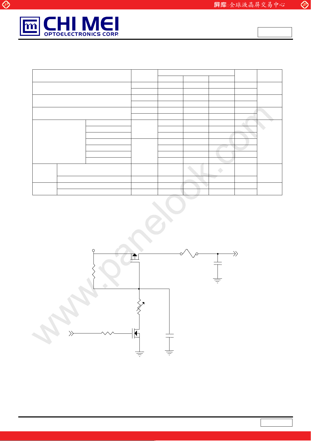
Item Symbol
Lamp Voltage VW
Power Supply Voltage VBL 0 30 V
Ё
Control Signal Level
Note (1) Permanent damage to the device may occur if maximum values are exceeded. Function operation
should be restricted to the conditions described under normal operating conditions.
Val ue
Min. Max.
Ё
5000 V
Unit Note
-0.3 7 V
RMS
(1)
(2), (3)
Note (2) No moisture condensation or freezing.
Note (3) The control signals include On/Off Control, Internal PWM Control, External PWM Control and
Internal/External PWM Selection.
9
One step solution for LCD / PDP / OLED panel application: Datasheet, inventory and accessory!
Version2.5
www.panelook.com
Page 10
Global LCD Panel Exchange Center
4. ELECTRICAL CHARACTERISTICS
www.panelook.com
Issued Date: Sep. 1, 2008
Model No.: V562D1-L02
Approval
4.1 TFT LCD MODULE
Parameter Symbol
Power Supply Voltage
Power Supply Ripple Voltage
Rush Current
Ta = 25 ± 2 ºC
Value
Min. Typ. Max.
V
17.1 18 18.9 V
CC1
V
4.5 5 5.5 V
CC2
V
- - 400 mV
RP1
V
200 mV
RP2
I
- - 4.5 A
RUSH1
I
- - 14 A
RUSH2
White - 1.9 2.5 A
I
CC1
- 1.5 - A
I
CC2
7.2 9 A
V 100 - 800 mV
95 100 105 ohm
T
Power Supply Current
DVI
Interface
Differential Input Voltage Single
Ended Amplitude
Receiver Resistor R
Black - 0.7 - A
Vertical Stripe
White - 5.4 - A
Black - 4.9 - A
Vertical Stripe - 5.5 A
V-Stripe-2column
Input High Threshold Voltage VIH 2.7 - 3.3 V CMOS
Interface
Input Low Threshold Voltage V
0 - 0.7 V
IL
Note: (1) The module should be always operated within the above ranges.
Unit Note
(1)
(2)
(3)
(4) (5)
(2) Measurement conditions:
+5V or +18V
+5.0V or
R1
1k
Q1 Si4485DY
Vcc 1 or
FUSE
C3
1uF
Vcc2
(LCD Module Input)
VR1
(Low to High)
(Control Signal)
SW
R2
1K
47K
Q2
2N7002
C1
0.01uF
10
One step solution for LCD / PDP / OLED panel application: Datasheet, inventory and accessory!
Version2.5
www.panelook.com
Page 11
Global LCD Panel Exchange Center
www.panelook.com
Issued Date: Sep. 1, 2008
Model No.: V562D1-L02
Approval
Vcc rising time is at least 470μs
0.9Vcc
0.1Vcc
GND
470μs
(3)The specified power supply current is under the conditions at Vcc1 = 18 V, Vcc2 = 5 V, Ta = 25 ± 2 ºC,
f
= 60 Hz, whereas a power dissipation check pattern below is displayed.
v
a. White Pattern
b. Black Pattern
c. Vertical Stripe Pattern
B
B
R
R
R
Active Area Active Area
G
G
G
R R
G
Active Area
(4) The electrical characteristics of DVI are specified in the DVI specification of DDWG.
(5) The receiver shall reproduce a test data stream, with pixel error rate
input amplitude illustrate by the eye diagram.
R
G
B
B
B
B
B
R
G
B
R
R
G
B
R
G
B
910−
, when presented with
11
One step solution for LCD / PDP / OLED panel application: Datasheet, inventory and accessory!
Version2.5
www.panelook.com
Page 12
Global LCD Panel Exchange Center
ˋ˃˃
˄˃˃
˃
ˀ˄˃˃
˗˼˹˹˸˸˼˴˿ʳ˔˿˼˷˸ʳʻ˩ʼ
ˀˋ˃˃
www.panelook.com
Issued Date: Sep. 1, 2008
Model No.: V562D1-L02
Approval
˃ˁ˅ˈ ˃ˁˆ ˃ˁˊ ˃ˁˊˈ˃ ˄
ˡ˴˿˼˸˷ʳ˧˼˸
˔˵˿˸ʳ˘˸ʳ˗˼˴˺˴ʳˠ˴˾ʳ˴ʳ˧ˣˆ
4.2 BACKLIGHT UNIT
4.2.1 CCFL (Cold Cathode Fluorescent Lamp) CHARACTERISTICS (Ta=25
Parameter Symbol
Lamp Voltage VW
Min. Typ. Max.
- 1728 -
Lamp Current IL 5.5 6.0 6.5 mA
- - 2550
Lamp Starting Voltage VS
- - 2350
Operating Frequency Fo 40 60 80 KHz (3)
Lamp Life Time LBL - 50000 - Hrs (4)
Value
2кккк
)
Unit Note
V
I
RMS
RMS
(2), Ta = 0 ºC
V
RMS
V
(2), Ta = 25 ºC
RMS
=5.7mA
L
(1)
4.2.2 INVERTER CHARACTERISTICS (Ta=25
Parameter Symbol
Power Consumption
P
- 315 330 W (5), IL = 6.0mA
BL
Power Supply Voltage VBL 22.8 24.0 25.2 VDC
Power Supply Current IBL - 13.13 13.75 A Non Dimming
Input Ripple Noise - - - 500 mV
Oscillating Frequency FW 47 50 53 kHz
Dimming frequency FB 150 160 180 Hz
Minimum Duty Ratio D
- 20 - %
MIN
Note (1) Lamp current is measured by utilizing high frequency current meters as shown below:
Min. Typ. Max.
2кккк
)
Val ue
Unit Note
VBL=22.8V
P-P
Note (2) The lamp starting voltage V
should be applied to the lamp for more than 1 second after startup.
S
Otherwise the lamp may not be turned on.
12
One step solution for LCD / PDP / OLED panel application: Datasheet, inventory and accessory!
Version2.5
www.panelook.com
Page 13
Global LCD Panel Exchange Center
Note (3) The lamp frequency may produce interference with horizontal synchronous frequency of the
display input signals, and it may result in line flow on the display. In order to avoid interference, the
lamp frequency should be detached from the horizontal synchronous frequency and its harmonics
as far as possible.
Note (4) The life time of a lamp is defined as when the brightness is larger than 50% of its original value and
the effective discharge length is longer than 80% of its original length (Effective discharge length is
defined as an area that has equal to or more than 70% brightness compared to the brightness at
the center point of lamp.) as the time in which it continues to operate under the condition at Ta = 25
2к
and IL = 5.5 ~ 6.5mA rms.
www.panelook.com
Issued Date: Sep. 1, 2008
Model No.: V562D1-L02
Approval
Note (5) The power supply capacity should be higher than the total inverter power consumption P
the pulse width modulation (PWM) mode was applied for backlight dimming, the driving current
changed as PWM duty on and off. The transient response of power supply should be considered
for the changing loading when inverter dimming.
Note (6) The measurement condition of Max. value is based on 56" backlight unit under input voltage 24V
, average lamp current 6.3 mA and lighting 30 minutes later.
. Since
BL
13
One step solution for LCD / PDP / OLED panel application: Datasheet, inventory and accessory!
Version2.5
www.panelook.com
Page 14

Global LCD Panel Exchange Center
www.panelook.com
Issued Date: Sep. 1, 2008
Model No.: V562D1-L02
Approval
Inverter
(Master)
a
1
2
a
a
1
2
a
a
1
2
a
a
1
2
a
a
1
2
a
a
1
2
a
a
1
2
a
a
1
2
a
HV (White -)
HV(Blue -)
HV (White +)
HV(Blue +)
HV (White -)
HV(Blue -)
HV (White +)
HV(Blue +)
HV (White -)
HV(Blue -)
HV (White +)
HV(Blue +)
HV (White -)
HV(Blue -)
HV (White +)
HV(Blue +)
A
A
A
A
A
A
A
A
A
A
A
A
A
A
A
A
HV (Pink +)
HV (White +)
HV (Pink -)
HV (White -)
HV (Pink +)
HV (White +)
HV (Pink -)
HV (White -)
HV (Pink +)
HV (White +)
HV (Pink -)
HV (White -)
HV (Pink +)
HV (White +)
HV (Pink -)
HV (White -)
A
b
1
2
A
b
1
A
b
2
A
b
1
A
b
2
A
b
A
b
1
2
A
b
A
b
1
A
b
2
A
b
1
A
b
2
1
A
b
2
A
b
A
b
1
2
A
b
Inverter
(Slave 2)
Inverter
(Slave 1)
LCD Module
a
1
2
a
1
a
2
a
1
a
2
a
a
1
2
a
a
1
2
a
a
1
2
a
a
1
2
a
1
a
2
a
HV (White -)
HV(Blue -)
HV (White +)
HV(Blue +)
HV (White -)
HV(Blue -)
HV (White +)
HV(Blue +)
HV (White -)
HV(Blue -)
HV (White +)
HV(Blue +)
HV (White -)
HV(Blue -)
HV (White +)
HV(Blue +)
A
A
A
A
A
A
A
A
A
A
A
A
A
A
A
A
HV (Pink +)
HV (White +)
HV (Pink -)
HV (White -)
HV (Pink +)
HV (White +)
HV (Pink -)
HV (White -)
HV (Pink +)
HV (White +)
HV (Pink -)
HV (White -)
HV (Pink +)
HV (White +)
HV (Pink -)
HV (White -)
A
b
1
A
b
2
A
b
1
2
A
b
A
b
1
2
A
b
A
b
1
A
b
2
A
b
1
A
b
2
A
b
1
A
b
2
A
b
1
A
b
2
A
b
1
2
A
b
Inverter
(Slave 3)
14
One step solution for LCD / PDP / OLED panel application: Datasheet, inventory and accessory!
Version2.5
www.panelook.com
Page 15
Global LCD Panel Exchange Center
X
)
)
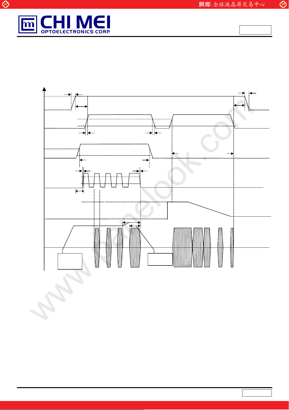
4.2.3 INVERTER INTERTFACE CHARACTERISTICS
Parameter Symbol
On/Off Control Voltage
Internal/External PWM
Select Voltage
Voltage
External PWM Control
Voltage
VBL Rising Time Tr1 웎 30 웎 50 ms
VBL Falling Time Tf1 웎 30 웎 50 ms
Control Signal Rising Time Tr
Control Signal Falling Time Tf
PWM Signal Rising Time T
PWM Signal Falling Time T
Input impedance RIN
BLON Delay Time Ton
BLON Off Time T
ON
OFF
HI
LO
MA
MIN
HI 2.0
LO
V
V
V
V
PW MR
BLON
IPWM
EPWM
PW MF
www.panelook.com
Te st
Condition
SEL
V
V
off
Ё
Ё
Ё
Ё
= L
SEL
= H
SEL
Ё
Ё
Ё
Ё
Ё
Ё
1 Ё
Ё
1 Ё
Val ue
Min. Typ. Max.
2.0
0
2.0
0
Ё Ё
Ё
0
Ё
Ё
Ё
Ё
1
Ё
Ё
Ё
Ё
0
Ё
Ё
Ё
Ё
Ё
Ё
Ё
5.0 V
0.8 V
5.0 V
-
0.8 V
3.0 V maximum duty ratioInternal PWM Control
Ё
5.0 V duty on, Note(4
0.8 V duty off, Note(4
100 ms
100 ms
50 us
50 us
Ё
Ё
Ё
Issued Date: Sep. 1, 2008
Model No.: V562D1-L02
Approval
Unit Note
Vminimum duty ratio
MӨ
ms
ms
Note (1) The SEL signal should be valid before backlight turns on by BLON signal. It is inhibited to change
the internal/external PWM selection (SEL) during backlight turn on period.
Note (2) The power sequence and control signal timing are shown in the following figure.
Note (3) The power sequence and control signal timing must follow the figure below. For a certain reason,
the inverter has a possibility to be damaged with wrong power sequence and control signal timing.
Note (4) EPWM duty ratio without inverter shut down is 0~95 % and 100%.
15
One step solution for LCD / PDP / OLED panel application: Datasheet, inventory and accessory!
Version2.5
www.panelook.com
Page 16
Global LCD Panel Exchange Center
www.panelook.com
Issued Date: Sep. 1, 2008
Model No.: V562D1-L02
Approval
V
V
V
V
BL
BLON
V
SEL
EPWM
IPWM
Tr1
2.0V
0.8V
2.0V
0.8V
2.0V
0.8V
3.0V
Ton
Backlight on duration
Tr
Ext. Dimming Function
T
PWMR
PWM
T
T
Tf
Int. Dimming Function
PWMF
0
0
0
0
0
Tf1
Toff
V
W
External
PWM
Period
External
PWM Duty
100%
Minimun
Duty
16
One step solution for LCD / PDP / OLED panel application: Datasheet, inventory and accessory!
Version2.5
www.panelook.com
Page 17

Global LCD Panel Exchange Center
)
www.panelook.com
Issued Date: Sep. 1, 2008
Model No.: V562D1-L02
Approval
5. BLOCK DIAGRAM
5.1 TFT LCD MODULE
1_Data0(+/-)
1_Data1(+/-)
1_Data2(+/-)
1_Clock(+/-)
2_Data0(+/-)
2_Data1(+/-)
-
2_Data2(+/-)
2_Clock(+/-)
3_Data0(+/-)
3_Data1(+/-)
3_Data2(+/-)
3_Clock(+/-)
4_Data0(+/-)
4_Data1(+/-)
4_Data2(+/-)
4_Clock(+/-)
Vcc1
Vcc2
GND
VBL
GND
.
SEL
E_PWM
I_PWM
BLON
CN9.
(74320-1004
(Molex))
(74320-1004
(Molex))
(74320-1004
(Molex)
(74320-1004
(Molex))
POWER CONNECTOR
(S20B-PHDSS-B(LF)(SN
CONNECTOR
CN1:S14B-PH-SM4-TB
(D)(LF) or equivalent
VBL
GND
CONNECTOR
CN2:S12B-PH-SM4-TB
(D)(LF) or equivalent
CONNECTOR
INPUT
FRAME
CONNECTOR
INPUT
BUFFER
TIMING
CONNECTOR
INPUT
CONNECTOR
INPUT
)(JST))
INVERTER
(Master)
CN4,CN6: 528521070 (Molex)
INVERTER
(Slave)
CONTROLLER
CN8-CN23:SM02 (12.0)B-BHS-1-TB(LF)(JST)
SCAN DRIVER
DC/DC CONVERTER
& REFERENCE
VOLTAGE
GENERATOR
CN3,CN5: 528521070 (Molex)
or equivalent
BACKLIGHT
UNIT
CN5,CN7: 528521070 (Molex)
DATA DRIVER (RSDS)
TFT LCD PANEL
(3840x3x2160)
DATA DRIVER(RSDS
INVERTER
CONNECTOR
CN2:S12B-PH-SM4-TB
(D)(LF) or equivalent
(Slave)
INVERTER
CONNECTOR
CN2:S12B-PH-SM4-TB
(D)(LF) or equivalent
(Slave)
SCAN DRIVER
VBL
GND
VBL
GND
17
One step solution for LCD / PDP / OLED panel application: Datasheet, inventory and accessory!
Version2.5
www.panelook.com
Page 18

Global LCD Panel Exchange Center
y
y
y
y
y
y
y
y
(3)
www.panelook.com
6. LCD INPUT TERMINAL PIN ASSIGNMENT
6.1 TFT LCD MODULE DVI INPUT
CN3, CN4, CN5, CN6 Connector Pin Assignment
Pin Signal Assignment Pin Signal Assignment Pin Signal Assignment
1 T.M.D.S Data2- 9 T.M.D.S Data1- 17 T.M.D.S Data0-
2 T.M.D.S Data2+ 10 T.M.D.S Data1+ 18 T.M.D.S Data0+
3 T.M.D.S Data2/4 shield 11 T.M.D.S Data1/3 shield 19 T.M.D.S Data0/5 shield
4 No Connect 12 No Connect 20 No Connect
5 No Connect 13 No Connect 21 No Connect
6 DDC Clock 14 +5V Power 22 T.M.D.S Clock shield
7 DDC Data 15 Ground(for +5V) 23 T.M.D.S Clock+
Issued Date: Sep. 1, 2008
Model No.: V562D1-L02
Approval
8 No Connect 16 Hot Plug Detect 24 T.M.D.S Clock-
C1 No Connect C2 No Connect C3 No Connect
C4 No Connect C5 No Connect
Note:(1) CN3, CN4, CN5, CN6 Connector part no.: 74320-1004 (Molex) or equivalent.
(2) The DVI pin assignment is specified in the DVI specification of DDWG.
6.2 TFT LCD MODULE POWER INPUT
CN9 Connector Pin Assignment
Pin No. S
1 VIN +18.0V power suppl
2 VIN +18.0V power suppl
3 V5VC +5.0V power suppl
4 V5VC +5.0V power suppl
5 V5VC +5.0V power suppl
6 NC Not connection
7 V5VC +5.0V power suppl
8 NC Not connection
9 V5VC +5.0V power suppl
10 NC Not connection
11 GND Ground
12 NC Not connection
13 GND Ground
14 NC Not connection
15 GND Ground
16
17 GND Ground
18
19
20 GND Ground
mbol Description Note
ODSEL
GND Ground
GND Ground
Overdrive Lookup Table Selection
Note: (1) CN9 connector part no.: S20B-PHDSS-B(LF)(SN), JST(
(2) CN10 is just only for CMO internal testing.
ֲءᚘထጤ),ᐚຏጤ
18
One step solution for LCD / PDP / OLED panel application: Datasheet, inventory and accessory!
or equivalent.
Version2.5
www.panelook.com
Page 19

Global LCD Panel Exchange Center
www.panelook.com
Issued Date: Sep. 1, 2008
Model No.: V562D1-L02
Approval
(3)
(4) “L” and “H” operation in (3) could follow “CMOS Interface” in Section 4.1.
6.3 BACKLIGHT UNIT
The pin configuration for the housing and the leader wire is shown in the table below.
Note (1) The backlight interface housing for high voltage side is a model BHR-04VS-1, manufactured by
1 HV(White)
2 HV(Pink)
ODSEL
accordance to the frame rate to optimize image quality.
(Overdrive Lookup Table Selection). The overdrive lookup table should be selected in frame
ODSEL Note
L Lookup table was optimized for 60Hz frame rate.
H Lookup table was optimized for 50Hz frame rate.
CN8-CN23: BHR-04VS-1 (JST).
Pin Name Description Wire Color
1 HV High Voltage Pink
2 HV High Voltage White
JST.The mating header on inverter part number is SM02(12.0)B-BHS-1-TB(LF).
1 HV(Pink)
2
HV(White)
1
Ϥ
2
Ϥ
1 HV(White)
2 HV(Pink)
1 HV(White)
2 HV(Pink)
1
HV(Pink)
2 HV(White)
1 HV(Pink)
2 HV(White)
≈
31
Ϥ
32
Ϥ
19
One step solution for LCD / PDP / OLED panel application: Datasheet, inventory and accessory!
Version2.5
www.panelook.com
Page 20

Global LCD Panel Exchange Center
6.4 INVERTER UNIT
CN1 (Master, Header): S14B-PH-SM4-TB (D)(LF)(JST) or equivalent
Pin No. Symbol Description
1
2
3
4
5
6
7
8
9
10
11
12 E_PWM
13 I_PWM
14 BLON Backlight on/off control
VBL +24V
GND GND
Internal/external PWM selection
SEL
High : external dimming
Low : internal dimming
External PWM control signal
E_PWM should be connected to ground when internal PWM was selected
(SEL = Low).
Internal PWM Control Signal
I_PWM should be connected to ground when external PWM was selected
(SEL = High).
power input
DC
www.panelook.com
Issued Date: Sep. 1, 2008
Model No.: V562D1-L02
Approval
CN2 (Slave, Header): S12B-PH-SM4-TB (D)(LF)(JST) or equivalent
Pin No. Symbol Description
1
2
3
4
5
6
7
8
9
10
11
12 NC NC
CN8-CN15 (Master, Header), CN16-CN23 (Slave, Header): SM02 (12.0) B-BHS-1-TB (LF)(JST) or equivalent
Pin No. Symbol Description
1
2
VBL +24V
GND GND
NC NC
CCFL HOT
CCFL HOT
CCFL high voltage
CCFL high voltage
power input
DC
20
One step solution for LCD / PDP / OLED panel application: Datasheet, inventory and accessory!
Version2.5
www.panelook.com
Page 21

Global LCD Panel Exchange Center
CN3-CN4 (Master, Header), CN5-CN7 (Slave, Header): 528521070 (Molex)
Pin No. Symbol Description
1 Board to Board
2
3
4
5
6
7
8
9
10
Note (1) Floating of any control signal is not allowed.
Control
Signal
Board to Board
Board to Board
Board to Board
Board to Board
Board to Board
Board to Board
Board to Board
Board to Board
Board to Board
www.panelook.com
Issued Date: Sep. 1, 2008
Model No.: V562D1-L02
Approval
21
One step solution for LCD / PDP / OLED panel application: Datasheet, inventory and accessory!
Version2.5
www.panelook.com
Page 22

Global LCD Panel Exchange Center
www.panelook.com
Issued Date: Sep. 1, 2008
Model No.: V562D1-L02
Approval
6.5 BLOCK DIAGRAM OF IMAGE SIGNAL
The video picture (3840x2160) should be divided into four parts: the left up side (1920x1080), the left down side
(1920x1080), the right up side(1920x1080) and the right down side(1920x1080). Signals of these four parts should
be delivered into the module individually through each single-DVI. And the protocol of DVI is specified in the DVI
specification of DDWG.
1/3 frame
buffer
Note: (1) It must be “synchronous” mutually between signals from CN3 and CN4.
(2) It must be “synchronous” mutually between signals from CN5 and CN6.
CN5 CN6 CN3 CN4
CN 9 CN10
CC Board
(3) It exists 1/3 frame buffer (i.e. buffer =1/3 x 1920 x1080 pixels) between (CN3/CN4) and (CN5/CN6)
(4) Signals of CN4 and CN6 must always be delivered to keep all of the power that’s necessary turned on
normally during the operation.
(5) “Synchronous” written in (1) and (2) is defined as a time difference smaller than 7 CLKs.
22
One step solution for LCD / PDP / OLED panel application: Datasheet, inventory and accessory!
Version2.5
www.panelook.com
Page 23

Global LCD Panel Exchange Center
6.6 DVI SIGNAL LIST
Signal Name Signal Description Note
T.M.D.S. Signals
T.M.D.S. Clock + & - T.M.D.S. clock differential pair.
T.M.D.S. Clock Shield Shield for T.M.D.S. clock differential pair.
T.M.D.S. Data0 + & - T.M.D.S. link #0 channel #0 differential pair.
T.M.D.S. Data0/5 Shield Shared shield for T.M.D.S. link #0 channel #0 and link #1 channel #2.
T.M.D.S. Data1 + & - T.M.D.S. link #0 channel #1 differential pair.
T.M.D.S. Data2/4 Shield Shared shield for T.M.D.S. link #0 channel #2 and link #1 channel #1.
T.M.D.S. Data2 + & - T.M.D.S. link #0 channel #2 differential pair.
www.panelook.com
Issued Date: Sep. 1, 2008
Model No.: V562D1-L02
Approval
T.M.D.S. Data1/3 Shield Shared shield for T.M.D.S. link #0 channel #1 and link #1 channel #0.
T.M.D.S. Data3 + & - T.M.D.S. link #1 channel #0 differential pair.
T.M.D.S. Data4 + & - T.M.D.S. link #1 channel #1 differential pair.
T.M.D.S. Data5 + & - T.M.D.S. link #1 channel #2 differential pair.
Control Signals
Hot Plug Detect(HPD) Signal is driven by monitor to enable the system to identify the
presence of a monitor.
DDC Data The data line for the DDC interface.
DDC Clock The clock line for the DDC interface
+5V Power +5 volt signal provided by the system to enable the monitor to
provide EDID data when the monitor circuitry is not powered.
Ground (for +5V) Ground reference for +5 volt power pin. Used as return by Hsync and
Vsync Signals.
Analog Signals
Analog Red Analog Red signal.
Analog Green Analog Green signal.
(1)
Analog Blue Analog Blue signal.
Analog Horizontal Sync Horizontal synchronization signal for the analog interface.
Analog Vertical Sync Vertical synchronization signal for the analog interface.
Analog Ground Common ground for analog signals. Used as a return for analog red,
green and blue signals only.
Note (1) No using.
(2)The DVI signal list is specified in the DVI specification of DDWG.
23
One step solution for LCD / PDP / OLED panel application: Datasheet, inventory and accessory!
(1)
Version2.5
www.panelook.com
Page 24

Global LCD Panel Exchange Center
pip
6.7 DVI LINK TIMING REQUIREMENTS
www.panelook.com
Issued Date: Sep. 1, 2008
Model No.: V562D1-L02
Approval
˜ʳ
˦˸˴
˧ˁˠˁ˗ˁ˦ˁʳ
˟˼˾
˗˘
˗˴˴ʳ˃
˗˴˴ʳ˄
˗˴˴ʳ˅
˴˶˼˸ʳ˼˷˸ʳ˸˺˼ ˴˶˼˸ʳ˼˷˸ʳ˸˺˼
˕˟˨ˮˊˍ˃˰
˺˸˷ ˺˸˷
˚˥ˡˮˊˍ˃˰
˥˘˗ˮˊˍ˃˰
˺˸˷
˸˶˷˸˷ʳ˕˟˨
˸˶˷˸˷ʳ˚˥ˡ
˸˶˷˸˷ʳ˥˘˗
˼˴˶˼˸˂˵˿˴˷ʳ˸˺˼
t
B
˺˸˷
˛˦ˬˡ˖ʿ˩˦ˬˡ˖
˺˸˷
˖˧˟˃ʿ˖˧˟˄
˺˸˷
˖˧˟˅ʿ˖˧˟ˆ
t
E
˸˶˷˸˷ʳ˛˦ˬˡ˖ʿ˩˦ˬˡ˖
˸˶˷˸˷ʳ˖˧˟˃ʿ˖˧˟˄
˸˶˷˸˷ʳ˖˧˟˃ʿ˖˧˟˄
t
E
˕˟˨ˮˊˍ˃˰
˚˥ˡˮˊˍ˃˰
˺˸˷˺˸˷
˥˘˗ˮˊˍ˃˰
˺˸˷
t
E
˸˶˷˸˷ʳ˕˟˨
˸˶˷˸˷ʳ˚˥ˡ
˸˶˷˸˷ʳ˥˘˗
t
E
t
B
˴˶˼˸ʳ˼˷˸ʳ˸˺˼
˥˸˶˸˸˷ʳ
˦˸˴
˗˘
˕˟˨ˮˊˍ˃˰
˶˴ʳ˛˦ˬˡ˖ʿ˩˦ˬˡ˖ ˶˴ʳ˛˦ˬˡ˖ʿ˩˦ˬˡ˖
˚˥ˡˮˊˍ˃˰
˥˘˗ˮˊˍ˃˰
˶˴ʳ˖˧˟˅ʿ˖˧˟ˆ
˼˴˿˼˷
˛˦ˬˡ˖ʿ˩˦ˬˡ˖
˼˴˿˼˷
˖˧˟˃ʿ˖˧˟˄
˼˴˿˼˷
˖˧˟˅ʿ˖˧˟ˆ
˕˟˨ˮˊˍ˃˰
˚˥ˡˮˊˍ˃˰
˶˴ʳ˖˧˟˃ʿ˖˧˟˄˶˴ʳ˖˧˟˃ʿ˖˧˟˄
˥˘˗ˮˊˍ˃˰
˶˴ʳ˖˧˟˅ʿ˖˧˟ˆ
Symbol Description Value Unit
t
Minimum duration blanking period required to ensure character
B
boundary recovery at the receiver. Blanking periods of this
128
T
pixel
duration must occur at least once every 50mS (20Hz).
t
Maximum encoding/serializer pipeline delay. 64
E
t
Maximum recovery/de-serizlizer
R
eline delay. Recovery timing
64
includes inter-channel skew, and is measured from the earliest
T
pixel
T
pixel
DE transition among the data channels.
Note: The DVI link timing requirements are specified in the DVI specification of DDWG.
24
One step solution for LCD / PDP / OLED panel application: Datasheet, inventory and accessory!
Version2.5
www.panelook.com
Page 25

Global LCD Panel Exchange Center
)
y
(2)
(3)
(4) (5)
y
k
y
k
7. INTERFACE TIMING
7.1 INPUT SIGNAL TIMING SPECIFICATIONS
The input signal timing specifications are shown as the following table and timing diagram.
Signal
DVI Receiver Clock (Single DVI
Vertical Active Display Term
(Single DVI,1920x1080 Active Area)
Horizontal Active Display Term
(Single DVI,1920x1080 Active Area)
Note: (1) Since this module is operated in DE only mode, Hsync and Vsync input signals should be set to
Frequenc
Frame Rate
Total Tv 1082 1090 1150 Th Tv=Tvd+Tvb
Displa
Blan
Total Th 2190 2200 2350 Tc Th=Thd+Thb
Displa
Blan
www.panelook.com
Issued Date: Sep. 1, 2008
Model No.: V562D1-L02
Approval
Item Symbol Min. Typ. Max. Unit Note
1/Tc 120 144 152 MH
Fr
Fr
5
6
47 50 53 Hz
57 60 63 Hz
Tvd - 1080 - Th
Tvb 2 10 70 Th
Thd - 1920 - Tc
Thb 270 280 430 Tc
Z
low logic level. Otherwise, this module would operate abnormally.
(2) The value of Typ. is based on 60Hz operation.
(3) (ODSEL) = (H). Please refer to Section 6.2 for detail information.
(4) (ODSEL) = (L). Please refer to Section 6.2 for detail information.
(5) The value of Max. will be modified beyond 60 Hz in the future due to the improvement from design.
˥˸˶˸˸˷ʳ
˦˸˴
˕˟˨ˮˊˍ˃˰
˛˦ˬˡ˖
˩˦ˬˡ˖
˚˥ˡˮˊˍ˃˰
˖˧˟˃
˖˧˟˄
˥˘˗ˮˊˍ˃˰
˖˧˟˅
˖˧˟ˆ
˖˟˞
˗˘
˧ˁˠˁ˗ˁ˦ˁʳ˴˼˸
˕˟˨ˮˊˍ˃˰
˛˦ˬˡ˖
˩˦ˬˡ˖
˚˥ˡˮˊˍ˃˰
˖˧˟˃
˖˧˟˄
˥˘˗ˮˊˍ˃˰
˖˧˟˅
˖˧˟ˆ
˖˟˞
˗ˮˊˍ˃˰
˖˃
˖˜
˗˘
˗ˮˊˍ˃˰
˖˃
˖˜
˗˘
˗ˮˊˍ˃˰
˖˃
˖˜
˗˘
˦˼˺˿˸ʳ˧ˁˠˁ˗ˁ˦ˁʳ˟˼˾
˘˶˷˸˂
˦˸˼˴˿˼˸
˘˶˷˸˂
˦˸˼˴˿˼˸
˘˶˷˸˂
˦˸˼˴˿˼˸
˗˴˴ʳ˃
˗˴˴ʳ˄
˗˴˴ʳ˅
˖˿˶˾
˧ˁˠˁ˗ˁ˦ˁʳ˸˶˸˼˸
˗ˮˊˍ˃˰
˖˃
˖˜
˗˸˶˷˸
˥˸˶˸˂
˗˘
˗ˮˊˍ˃˰
˖˃
˖˜
˗˸˶˷˸
˥˸˶˸˂
˗˘
˗ˮˊˍ˃˰
˖˃
˖˜
˗˸˶˷˸
˥˸˶˸˂
˗˘
˕˟˨ˮˊˍ˃˰
˛˦ˬˡ˖
˩˦ˬˡ˖
˗˘˃
˚˥ˡˮˊˍ˃˰
˖˧˟˃
˖˧˟˄
˗˘˄
˥˘˗ˮˊˍ˃˰
˖˧˟˅
˖˧˟ˆ
˗˘˅
Note: The single link T.M.D.S. channel map is specified in the DVI specification of DDWG.
25
One step solution for LCD / PDP / OLED panel application: Datasheet, inventory and accessory!
Version2.5
www.panelook.com
Page 26

Global LCD Panel Exchange Center
www.panelook.com
7.2 EXTENDED DISPLAY IDENTIFICATION DADA (EDID) STRUCTURE
Issued Date: Sep. 1, 2008
Model No.: V562D1-L02
Approval
Address No. bytes
00h
00h
01h
02h
03h
04h
05h
06h
07h
08h
08h
0Ah
0Ch
10h
11h
ˋˋˋˋʳʳʳʳ
ʳʳ ˄ʳ
ʳʳ ˄ʳ
ʳʳ ˄ʳ
ʳʳ ˄ʳ
ʳʳ ˄ʳ
ʳʳ ˄ʳ
ʳʳ ˄ʳ
ʳʳ ˄ʳ
˄˃
˄˃ʳʳʳʳ
˄˃˄˃
ʳʳ ˅ʳ
ʳʳ ˅ʳ
ʳʳ ˇʳ
ʳʳ ˄ʳ
ʳʳ ˄ʳ
ʳʳʳʳʳ
ʳ
Description Address No. bytes
Bytes Header
00h 1Dh
FFh 1Eh
FFh 1Fh
FFh 20h
FFh 21h
FFh 22h
FFh
00h 23h
Bytes Vender/Product Identification
ID Manufacturer Name 25h
ID Product Code
ID Serial Number 26h
Week of Manufacture 28h
Year of Manufacture 2Ah
1Ch
23h
24h
26h
ʳʳ ˄ʳ
ʳʳ ˄ʳ
ʳʳ ˄ʳ
ʳʳ ˄ʳ
ʳʳ ˄ʳ
ʳʳ ˄ʳ
ʳʳ ˄ʳ
ˆˆˆˆʳʳʳʳ
ʳʳ ˄ʳ
ʳʳ ˄ʳ
ʳʳ ˄ʳ
˄ˉ
˄ˉʳʳʳʳ
˄ˉ˄ˉ
ʳʳ ˅ʳ
ʳʳ ˅ʳ
ʳʳ ˅ʳ
ʳʳʳʳʳ
Bytes Established Timings
Bytes Standard Timing Identification
ʳ
Description
Red -y
Green -x
Green -y
Blue -x
Blue -y
White -x
White -y
Established Timings 1
Established Timings 2
Manufacturers Reserved Timings
Standard Timing Identification #1
Standard Timing Identification #2
Standard Timing Identification #3
12h
12h
13h
14h
14h
15h
16h
17h
18h
19h
19h
1Ah
˅˅˅˅ʳʳʳʳ
Bytes EDID Structure Version/Revision
ʳʳ ˄ʳ
ʳʳ ˄ʳ
ˈˈˈˈʳʳʳʳ
ʳʳ ˄ʳ
ʳʳ ˄ʳ
ʳʳ ˄ʳ
ʳʳ ˄ʳ
ʳʳ ˄ʳ
˄˃
˄˃ʳʳʳʳ
˄˃˄˃
ʳʳ ˄ʳ
ʳʳ ˄ʳ
Version # 2Eh
Revision # 30h
Bytes Basic Display Parameters/Features
Video Input Definition 34h
Max.Horizontal Image Size
Max.Vertical Image Size 36h
Display Transfer Characteristic
(Gamma) 48h
Feature Support 5Ah
Bytes Color Characteristics
Red / Green Low Bits
Blue / White Low Bits
2Ch
32h
36h
6Ch
7Eh
7Fh
ʳʳ ˅ʳ
ʳʳ ˅ʳ
ʳʳ ˅ʳ
ʳʳ ˅ʳ
ʳʳ ˅ʳ
ˊ˅
ˊ˅ʳʳʳʳ
ˊ˅ˊ˅
ʳ ʳ ˄ˋʳ
ʳ ʳ ˄ˋʳ
ʳ ʳ ˄ˋʳ
ʳ ʳ ˄ˋʳ
˄˄˄˄ʳʳʳʳ
˄˄˄˄ʳʳʳʳ
Standard Timing Identification #4
Standard Timing Identification #5
Standard Timing Identification #6
Standard Timing Identification #7
Standard Timing Identification #8
Bytes Detailed Timing Descriptions
Detailed Timing Description #1 or
Monitor Descriptor.
Detailed Timing Description #2 or
Monitor Descriptor.
Detailed Timing Description #3 or
Monitor Descriptor.
Detailed Timing Description #4 or
Monitor Descriptor.
Byte Extension Flag
Byte Checksum
1Bh
Note: The EDID structure is specified in the EDID standard of VESA.
ʳʳ ˄ʳ
Red -x
ʳʳ ʳʳ
26
One step solution for LCD / PDP / OLED panel application: Datasheet, inventory and accessory!
Version2.5
www.panelook.com
Page 27

Global LCD Panel Exchange Center
7.3 EXTENDED DISPLAY IDENTIFICATION DADA (EDID) CODE
˃ʳ
˃ʳ ʳʳ˄ʳ
˄ʳ ʳʳ˅ʳ
˅ʳ ʳʳˆʳ
ADDR
˃ʳ˃ʳ
˄ʳ˄ʳ
˅ʳ˅ʳ
ˆʳ ʳʳˇʳ
ˆʳˆʳ
www.panelook.com
ˇʳ ʳʳˈʳ
ˈʳ ʳʳˉʳ
ˈʳˈʳ
ˉʳ ʳ
ˉʳˉʳ
ʳ
ˇʳˇʳ
000000 00 FF FF FF FF FF FF 00 – 3A C4 10 A0 64 00 00 00
000010 31 0F 01 03 80 34 21 78 – EE EE 50 A3 54 4C 9B 26
000020 0F 50 54 00 00 00 01 01 - 01 01 01 01 01 01 01 01
000030 01 01 01 01 01 01 34 38 - 80 18 71 38 0A 40 10 50
000040 12 00 54 30 34 00 00 18 – D6 2E 80 18 71 38 0A 40
000050 10 50 12 00 54 30 34 00 - 00 18 F6 2C 80 18 71 77
000060 0A 40 10 50 12 00 54 30 - 34 00 00 18 00 00 00 00
000070 00 00 00 00 00 00 00 00 - 00 00 00 00 00 00 00 38
7 - 8
Issued Date: Sep. 1, 2008
Model No.: V562D1-L02
Approval
ˌʳ
ˌʳ ʳ
ˌʳˌʳ
ʳ
A B C D E F
Note:(1) The EDID code implies 60Hz, 50Hz and 48Hz.
27
One step solution for LCD / PDP / OLED panel application: Datasheet, inventory and accessory!
Version2.5
www.panelook.com
Page 28

Global LCD Panel Exchange Center
7.4 POWER ON/OFF SEQUENCE
To prevent a latch-up or DC operation of LCD module, the power on/off sequence should be
followed as the diagram below.
ˣ˸ʳ˦˿
ˣ˸ʳ˦˿
ˣ˸ʳ˦˿ˣ˸ʳ˦˿
˩˶˶˄ʿʳ˩˶˶˅
www.panelook.com
˃ˁˌ˩˶˶ ˄
Issued Date: Sep. 1, 2008
Model No.: V562D1-L02
Approval
˃ˁˌ˩˶˶ ˄
˃ˁˈЉ˧˄Љ˄˃ʻ˩˶˶˄ʼ
˃ˁˈЉ˧ˊЉ˄˃ʻ˩˶˶˅ʼ
˃Љ˧ˋЉˈ˃
˃Љ˧˅Љˈ˃
˃Љ˧ˆЉˈ˃
ˈ˃˃Љ˧ˇ
˦˼˺˴˿
˦˼˺˴˿
˦˼˺˴˿˦˼˺˴˿
˕˴˶˾˿˼˺˻ʳʻ˥˸˶˸˷˸˷ʼ
ˈ˃˃Љ˧ˈ
˄˃˃Љ˧ˉ
˃˩
˃˩
˃˩
˃ˁ˄˩˶˶ ˄
˧˄
˧˄
˃ˁˌ˩˶˶ ˅
˧˄˧˄
˃ˁ˄˩˶˶ ˅
˧ˊ
˧ˊ
˧ˊ˧ˊ
˧ˋ
˧ˋ
˧ˋ˧ˋ
˧˅
˧˅
˧˅˧˅
˩˔˟˜˗
ˣ˸ʳˢ ˣ˸ʳˢ˹˹
ˈ˃ʸ ˈ˃ʸ
˧ˈ
˧ˈ ˧ˉ
˧ˈ˧ˈ
ˣ˸ʳˢˡ˂ˢ˙˙ʳ˦˸˸˶˸
ˣ˸ʳˢˡ˂ˢ˙˙ʳ˦˸˸˶˸
ˣ˸ʳˢˡ˂ˢ˙˙ʳ˦˸˸˶˸ˣ˸ʳˢˡ˂ˢ˙˙ʳ˦˸˸˶˸
˃ˁˌ˩˶˶ ˅
˧ˉ
˧ˉ˧ˉ
˧ˆ
˧ˆ
˧ˆ˧ˆ
˃ˁ˄˩˶˶ ˄
˃ˁ˄˩˶˶˅
˧ˇ
˧ˇ
˧ˇ˧ˇ
Note : (1) The supplied voltage of the external system for the module input should follow the definition of Vcc1,2.
(2) Apply the lamp voltage within the LCD operation range. When the backlight turns on before the LCD
operation or the LCD turns off before the backlight turns off, the display may momentarily become
abnormal screen.
(3) In case of Vcc1,2 is in off level, please keep the level of input signals on the low and avoid floating.
(4) T4 should be measured after the module being fully discharged between power off and on period.
(5) Interface signal shall not be kept at high impedance when the power is on.
28
Version2.5
One step solution for LCD / PDP / OLED panel application: Datasheet, inventory and accessory!
www.panelook.com
Page 29

Global LCD Panel Exchange Center
8. OPTICAL CHARACTERISTICS
8.1 TEST CONDITIONS
Item Symbol Value Unit
Ambient Temperature Ta
Ambient Humidity Ha
Supply Voltage VCC 5.0 V
Input Signal According to typical value in "3. ELECTRICAL CHARACTERISTICS"
Lamp Current IL
Oscillating Frequency (Inverter) FL
Frame Rate Fr 60 Hz
8.2 OPTICAL SPECIFICATIONS
The relative measurement methods of optical characteristics are shown in 8.2 Notes. The following items
www.panelook.com
25±2
50±10
6.0±0.5
50±3
Issued Date: Sep. 1, 2008
Model No.: V562D1-L02
Approval
o
C
%RH
mA
KHz
should be measured under the test conditions described in 8.1 and stable environment shown in Note (6).
Item Symbol Condition Min. Typ. Max. Unit Note
Contrast Ratio CR 900 1200 - Note (2)
Gray to
Response Time
6.5 ms Note (3)
gray
Center Luminance of White L
Average Luminance of White
White Variation
Cross Talk CT 4 % Note (5)
C
L
400 450 - cd/m2Note (4)
AVE
δW
=0°, θY =0°
θ
x
Rx 0.651 -
Viewing angle at
450 500 cd/m2Note (4)
1.6 - Note (7)
Red
0.332
0.269
0.593
0.144
0.060
0.285
Typ.
+0.03
-
-
Note (6)
-
-
-
Color
Chromaticity
Green
Blue
Ry
Gx
Gy
Bx
By
Wx
normal direction
Typ.
-0.03
White
Wy
0.293
-
Color Gamut C.G
θx+
72 75 % NTSC
80 88
Horizontal
Viewing
θ
-
x
80 88
CR≥30
Angle
θY+
80 88
Vertical
θ
-
Y
80 88
29
One step solution for LCD / PDP / OLED panel application: Datasheet, inventory and accessory!
Deg. Note (1)
Version2.5
www.panelook.com
Page 30

Global LCD Panel Exchange Center
T
T
Note (1) Definition of Viewing Angle (θx, θy):
Viewing angles are measured by Eldim EZ-Contrast 160R
www.panelook.com
Issued Date: Sep. 1, 2008
Model No.: V562D1-L02
Approval
θX- = 90º
x-
6 o’clock
θ
y-
= 90º
y-
Note (2) Definition of Contrast Ratio (CR):
The contrast ratio can be calculated by the following expression.
Contrast Ratio (CR) = L255 / L0
L255: Luminance of gray level 255
Normal
θx = θy = 0º
θy- θy+
θx−
θx+
y+
12 o’clock direction
θ
y+
= 90º
x+
θX+ = 90º
L 0: Luminance of gray level 0
CR = CR (7), where CR (X) is corresponding to the Contrast Ratio of the point X at the figure in Note
(7).
Note (3) Definition of Gray to Gray Switching Time:
100%
90%
Optical
Response
10%
0%
Gray to gray
switching time
The driving signal means the signal of gray level 0, 63, 127, 191, 255.
Gray to gray average time means the average switching time of gray level 0 ,63,127,191,255 to each
ime
ime
Gray to gray
switching time
other.
30
One step solution for LCD / PDP / OLED panel application: Datasheet, inventory and accessory!
Version2.5
www.panelook.com
Page 31

Global LCD Panel Exchange Center
(
)
(
)
www.panelook.com
Issued Date: Sep. 1, 2008
Model No.: V562D1-L02
Approval
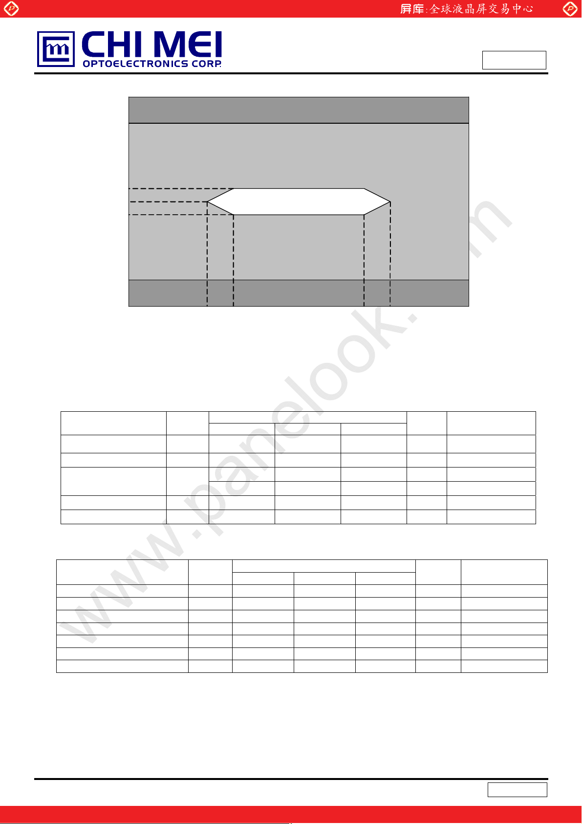
Note (4) Definition of Luminance of White (LC, L
Measure the luminance of gray level 255 at center point and 5 points
LC = L (7)
L
= [L (4)+ L (5)+ L (7)+ L (9)+ L (10)] / 5
AVE
Where L (x) is corresponding to the luminance of the point X at the figure in Note (7).
Note (5) Definition of Cross Talk (CT):
CT = | Y
– YA | / YA × 100 (%)
B
Where:
Y
= Luminance of measured location without gray level 0 pattern (cd/m2)
A
Y
= Luminance of measured location with gray level 0 pattern (cd/m2)
B
(0, 0)
Active Area
Y
(D/8,W/2)
A, L
Gray 128
Y
(D/2,7W/8)
A, D
Y
A, U
Y
A, R
(D,W)
):
AVE
(D/2,W /8)
(7D/8,W/2)
(D/4,W/4)
Y
(D/8,W/2)
B, L
Y
(D/2,7W/8)
B, D
0, 0
Active Area
Gray 0
Gray 0
Gray 128
Y
(D/2,W /8)
B, U
Y
(7D/8,W/2)
B, R
(3D/4,3W/4)
D,W
31
One step solution for LCD / PDP / OLED panel application: Datasheet, inventory and accessory!
Version2.5
www.panelook.com
Page 32

Global LCD Panel Exchange Center
Note (6) Measurement Setup:
The LCD module should be stabilized at given temperature for 1 hour to avoid abrupt
temperature change during measuring. In order to stabilize the luminance, the measurement
should be executed after lighting backlight for 1 hour in a windless room.
LCD Module
www.panelook.com
Issued Date: Sep. 1, 2008
Model No.: V562D1-L02
Approval
LCD Panel
Center of the Screen
Note (7) Definition of White Variation (δW):
Measure the luminance of gray level 255 at 13 points
δW = Maximum [L (1), L (2), L (3), L (4),
Display Color Analyzer
(Minolta CA210)
Light Shield Room
(Ambient Luminance < 2 lux)
ΕΕΕ
, L (13)] / Minimum [L (1), L (2), L (3), L (4),
D
ΕΕΕ
, L (13)]
D/10 9D/10
3D/10 5D/10 7D/10
W/10
1
2
3
10
5
: Test Point
8
13
X
X=1 to 13
4
7
W
3W /10
5W /10
6
Vertical Line
7W /10
9W /10
11
9
12
Active Area
32
Version2.5
One step solution for LCD / PDP / OLED panel application: Datasheet, inventory and accessory!
www.panelook.com
Page 33

Global LCD Panel Exchange Center
www.panelook.com
Issued Date: Sep. 1, 2008
Model No.: V562D1-L02
Approval
9. PRECAUTIONS
9.1 ASSEMBLY AND HANDLING PRECAUTIONS
(1) Do not apply rough force such as bending or twisting to the module during assembly.
(2) It is recommended to assemble or to install a module into the user’s system in clean working areas. The
dust and oil may cause electrical short or worsen the polarizer.
(3) Do not apply pressure or impulse to the module to prevent the damage of LCD panel and Backlight.
(4) Always follow the correct power-on sequence when the LCD module is turned on. This can prevent the
damage and latch-up of the CMOS LSI chips.
(5) Do not plug in or pull out the I/F connector while the module is in operation.
(6) Do not disassemble the module.
(7) Use a soft dry cloth without chemicals for cleaning, because the surface of polarizer is very soft and
easily scratched.
(8) Moisture can easily penetrate into LCD module and may cause the damage during operation.
(9) When storing modules as spares for a long time, the following precaution is necessary.
a. Do not leave the module in high temperature, and high humidity for a long time. It is highly
recommended to store the module with temperature from 0 to 35
condensation.
b. The module shall be stored in dark place. Do not store the TFT-LCD module in direct sunlight or
fluorescent light.
(10) When ambient temperature is lower than 10ºC, the display quality might be reduced. For example, the
response time will become slow, and the starting voltage of CCFL will be higher than that of room
temperature.
к
at normal humidity without
9.2 SAFETY PRECAUTIONS
(1) The startup voltage of a Backlight is approximately 1000 Volts. It may cause an electrical shock while
assembling with the inverter. Do not disassemble the module or insert anything into the Backlight unit.
(2) If the liquid crystal material leaks from the panel, it should be kept away from the eyes or mouth. In case
of contact with hands, skin or clothes, it has to be washed away thoroughly with soap.
(3) After the module’s end of life, it is not harmful in case of normal operation and storage.
9.3 SAFETY STANDARDS
The LCD module should be certified with safety regulations as follows:
(1) UL60950-1 or updated standard.
(2) IEC60950-1 or updated standard.
(3) UL60065 or updated standard.
(4) IEC60065 or updated standard.
33
One step solution for LCD / PDP / OLED panel application: Datasheet, inventory and accessory!
Version2.5
www.panelook.com
Page 34

Global LCD Panel Exchange Center
10. DEFINITION OF LABELS
10.1 CMO MODULE LABEL
The barcode nameplate is pasted on each module as illustration, and its definitions are as following explanation.
www.panelook.com
Issued Date: Sep. 1, 2008
Model No.: V562D1-L02
Approval
V562D1 -L02 Rev. XX
CHI MEI
OPTOELECTRONICS
X X X X X X X Y M D L N N N N
(a) Model Name: V562D1-L02
(b) Revision: Rev. XX, for example: A0, A1… B1, B2… or C1, C2…etc.
(c) Serial ID: X X
X X X X X Y M D L N N N N
Serial No.
Product Line
Year, Month, Date
CMO Internal Use
CMO Internal Use
Revision
E207943
MADE IN TAIWAN
RoHS
Serial ID includes the information as below:
(a) Manufactured Date: Year: 0~9, for 2000~2009
Month: 1~9, A~C, for Jan. ~ Dec.
Day: 1~9, A~Y, for 1
(b) Revision Code: Cover all the change
(c) Serial No.: Manufacturing sequence of product
(d) Product Line: 1 -> Line1, 2 -> Line 2, …etc.
CMO Internal Use
st
to 31st, exclude I ,O, and U.
34
One step solution for LCD / PDP / OLED panel application: Datasheet, inventory and accessory!
Version2.5
www.panelook.com
Page 35

Global LCD Panel Exchange Center
11. PACKAGE
11.1 PACKING SPECIFICATIONS
(1) 2 LCD TV modules / 1 Box
(2) Box dimensions : 1448(L) X 372 (W) X 901 (H)
(3) Weight : approximately 56Kg (2 modules per box)
(4) One protective film is attached on the LCD TV
11.2 PACKING METHOD
Figures 9-1 and 9-2 are the packing method
www.panelook.com
Issued Date: Sep. 1, 2008
Model No.: V562D1-L02
Approval
Anti-static Bag
4pcs Drier
Cushion(Bottom)
LCD TV Module
Carton
Carton Labe
4pcs Jo int
Figure.9-1 packing method
35
One step solution for LCD / PDP / OLED panel application: Datasheet, inventory and accessory!
Version2.5
www.panelook.com
Page 36

Global LCD Panel Exchange Center
Sea Transportation
Corner Protector:L1780*50mm*50mm
Corner Protector:L1130*50mm*50mm
Pallet:L1150*W1460*H140mm
Pallet Stack:L1150*W1460*H1942mm
Gross:353kg
www.panelook.com
Issued Date: Sep. 1, 2008
Model No.: V562D1-L02
Approval
PP Belt
PP Belt
Figure. 9-2 Packing method
36
One step solution for LCD / PDP / OLED panel application: Datasheet, inventory and accessory!
Version2.5
www.panelook.com
Page 37

Global LCD Panel Exchange Center
12. MECHANICAL CHARACTERISTIC
www.panelook.com
Issued Date: Sep. 1, 2008
Model No.: V562D1-L02
Approval
࡛ભሽٝڶૻֆ
CHI MEI
37
One step solution for LCD / PDP / OLED panel application: Datasheet, inventory and accessory!
Version2.5
www.panelook.com
Page 38

Global LCD Panel Exchange Center
www.panelook.com
Issued Date: Sep. 1, 2008
Model No.: V562D1-L02
Approval
࡛ભሽٝ ڶૻֆ
CHI MEI
38
One step solution for LCD / PDP / OLED panel application: Datasheet, inventory and accessory!
Version2.5
www.panelook.com
Page 39

Global LCD Panel Exchange Center
www.panelook.com
Issued Date: Sep. 1, 2008
Model No.: V562D1-L02
Approval
࡛ભሽٝ ڶૻֆ
CHI MEI
39
One step solution for LCD / PDP / OLED panel application: Datasheet, inventory and accessory!
Version2.5
www.panelook.com
Page 40

Global LCD Panel Exchange Center
www.panelook.com
Issued Date: Sep. 1, 2008
Model No.: V562D1-L02
Approval
ڻႝηިҽԖϦљ
CHI MEI
40
One step solution for LCD / PDP / OLED panel application: Datasheet, inventory and accessory!
Version2.5
www.panelook.com
Page 41

Global LCD Panel Exchange Center
Appendix 1 (CMO Guarantee List)
(1) If CMO changes the content in LCD module, CMO shall obtain Mitsubishi's approval in advance.
(2) If CMO changes the production facility and factory, CMO shall obtain Mitsubishi's approval in advance.
(3) CMO inspects panels before shipping them out, and CMO shall send Mitsubishi the inspection data.
(4) For EMI solution, put the conductive tapes on 4 sides.
(5) There must not be obstacle in the image display.
(6) There must not be “Low Temperature Noise”.
(7)
No gluing float of the “L-shape” flat-cable. Please refer to the figure on page 37.
(8) Customers could use this LCD module by “tilting” or “face up” without any problem except for OPT
performance slightly different from standard use. But please don't use this LCD module by portrait type.
(9) If any questions arise about criteria not mentioned in this spec, CMO and Mitsubishi shall discuss in good
www.panelook.com
Issued Date: Sep. 1, 2008
Model No.: V562D1-L02
Approval
faith to decide corrective action and new criteria based on mutual consent.
Appendix 2 (Service Parts Revision Description)
CC BoardΚPart No. 35-D017080, Rev.03
Tcon (CR) Board
Tcon (CL) Board
INVERTER
Κ
Part No. 35-D017058, Rev.06
Κ
Part No. 35-D017057, Rev.06
Κ
Part No. 27-D006305, Rev.2E (Rev.9)
Note:
Externals drawing of these service parts is referred in Reference 5.
41
One step solution for LCD / PDP / OLED panel application: Datasheet, inventory and accessory!
Version2.5
www.panelook.com
Page 42

Global LCD Panel Exchange Center
www.panelook.com
Appendix 3 (Part No./Revision/Modification Record of Parts)
Module
Revision (Date)
Item
B3
B4
B6
C1
Issued Date: Sep. 1, 2008
Model No.: V562D1-L02
Approval
C2
C2
(After 10/5)
C3
C4
LCD process
Liquid Crystal (LC)
Tcon (CR/CL)
CC Board
(Reference 1)
Inverter
(Part No.
27-D006305)
(Reference 2)
Board
2 cut
available
CR:Part No. 35-D015208, Rev.05
CL: Part No. 35-D015207, Rev.05
Part No. 35-D015667, Rev.02
Rev.1C
(Rev.7)
Rev.1D/
Rev.1E
(Rev.8/
Rev.9)
1 cut
available
2 cut
available
(Fine tune TFT/
CF total pitch)
(New BM mask for light leakage improving)
M52 M3
2 cut available
CR: Part No. 35-D017058, Rev.06
CL: Part No. 35-D017057, Rev.06
Part No. 35-D017080, Rev.03
Rev.1E
(Rev.9)
Rev.1E
(Rev.9)
P.S . R ew or k CP
points for 6.0 mA
lamp current.
P.S. Modif y resistors for 6.0
mA lamp current .
Rev.2E
(Rev.9)
CCFL (Lamp)
4 Sides Conductive Tape
for EMI Improve ment
Screw Number for
Fixing Frame of BLU
(Reference 3)
Pin Supporter
(Reference 4)
Sensor Holes on
BLU
Individual
(attached by glue)
The same
No
10
Adjustment of phosphor ratio for brightness enhancement
Yes (1.5 mm)
8
Combined with lamp supporter
W/O
10
Yes (0.8 mm)
Two
Holes
42
Version2.5
One step solution for LCD / PDP / OLED panel application: Datasheet, inventory and accessory!
www.panelook.com
Page 43

Global LCD Panel Exchange Center
www.panelook.com
Reference 1 (Modification Record of CC Board)
CC Board
Item
35-D015667/ Rev.02
Issued Date: Sep. 1, 2008
Model No.: V562D1-L02
Approval
35-D017080/ Rev.03
Refer to 1 on Picture 1
CN9
S20B-PHDSS-B(LF)(SN) (by JST) LM113P-020- TF1-3 (by UNE)
Change Reason: To increase the ability of each pin enduring current to increase safety.
Refer to 2 on Picture 1
OPAMP
Refer to Picture 1
Change Reason: Since LC is changed from M3 to M52,CMO need to change OPAMP which can be
capable of enduring larger voltage.
Refer to 3 on Picture 1
Resistor
Refer to Picture 1
Change Reason: To change the way of dividing voltage.
Refer to 4 on Picture 1
Tes t Po in t
Refer to Picture 1
Change Reason: To add test point offering a easy way for CMO’s internal EEPROM coding.
Refer to 5 on Picture 1
Capacitor
0603 1206
Change Reason: It will have shortage risk if 1206 is continuously used.
43
Version2.5
One step solution for LCD / PDP / OLED panel application: Datasheet, inventory and accessory!
www.panelook.com
Page 44

Global LCD Panel Exchange Center
p
Reference 2 (Modification Record of Inverter)
www.panelook.com
Issued Date: Sep. 1, 2008
Model No.: V562D1-L02
Approval
Inverter
Part No./Revision
27-D006305
Rev.1C
(Rev.7)
27-D006305
Rev.1D
(Rev.8)
27-D006305
Rev.1E
(Rev.9)
Item
27-D006305
Rev.1E (Rev.9)
(Rework CP
points for
6.0 mA lamp
current)
27-D006305
Rev.2E (Rev.9)
(Modify
resistors for
6.0 mA lamp
current)
(T301~T308, T401~T408)
Tran s former
EI-20.4
EI22.3
Change Reason:
(1)To increase the power rating of transformer while the temperature of device could be decreased as well to make reliability
better.
(2)Since(1), several parameters within the protective and feedback circuit will be modified to optimize the inverter
erformance.
CN3, CN4, CN5, CN6, CN7
7151-E10N(E&T)
(Color: Black)
528521070 (Molex)
(Color: White)
Change Reason: To avoid the shortage risk of 7151-E10N (E&T), no special functional concern for this change.
(C301, C303, C401, C403)
CP Points
Open
Short
Open
Change Reason: To change lamp current from 5.7 mA to 6.0mA(Short term solution).
(R330, R331, R430, R431)
Resistors
174 ohm 165 ohm
Change Reason: To change lamp current from 5.7 mA to 6.0mA(Long term solution).
44
One step solution for LCD / PDP / OLED panel application: Datasheet, inventory and accessory!
Version2.5
www.panelook.com
Page 45

Global LCD Panel Exchange Center
www.panelook.com
Reference 3 (Modification Record of Screw Number on BLU Frame)
Issued Date: Sep. 1, 2008
Model No.: V562D1-L02
Approval
B4
Other Revisions
45
One step solution for LCD / PDP / OLED panel application: Datasheet, inventory and accessory!
Version2.5
www.panelook.com
Page 46

Global LCD Panel Exchange Center
www.panelook.com
Issued Date: Sep. 1, 2008
Model No.: V562D1-L02
Approval
Reference 4 (Modification Record of Pin Supporter)
Combined with lamp supporter
᧢৵
Individual (attached by glue)
᧢ছ
46
One step solution for LCD / PDP / OLED panel application: Datasheet, inventory and accessory!
Version2.5
www.panelook.com
Page 47

Global LCD Panel Exchange Center
www.panelook.com
Issued Date: Sep. 1, 2008
Model No.: V562D1-L02
Approval
Reference 5 (
Externals Drawing of
Service Parts)
CC Board (DVI holder not included)
ڻႝηިҽԖϦљ
CHI MEI
47
One step solution for LCD / PDP / OLED panel application: Datasheet, inventory and accessory!
Version2.5
www.panelook.com
Page 48

Global LCD Panel Exchange Center
Tcon (CR) Board
www.panelook.com
Issued Date: Sep. 1, 2008
Model No.: V562D1-L02
Approval
ڻႝηިҽԖϦљ
CHI MEI
48
One step solution for LCD / PDP / OLED panel application: Datasheet, inventory and accessory!
Version2.5
www.panelook.com
Page 49

Global LCD Panel Exchange Center
Tcon (CL) Board
www.panelook.com
Issued Date: Sep. 1, 2008
Model No.: V562D1-L02
Approval
ڻႝηިҽԖϦљ
CHI MEI
49
One step solution for LCD / PDP / OLED panel application: Datasheet, inventory and accessory!
Version2.5
www.panelook.com
Page 50

Global LCD Panel Exchange Center
INVERTER (Master)
www.panelook.com
Issued Date: Sep. 1, 2008
Model No.: V562D1-L02
Approval
ڻႝηިҽԖϦљ
CHI MEI
50
One step solution for LCD / PDP / OLED panel application: Datasheet, inventory and accessory!
Version2.5
www.panelook.com
Page 51

Global LCD Panel Exchange Center
INVERTER (Slave)
www.panelook.com
Issued Date: Sep. 1, 2008
Model No.: V562D1-L02
Approval
ڻႝηިҽԖϦљ
CHI MEI
51
One step solution for LCD / PDP / OLED panel application: Datasheet, inventory and accessory!
Version2.5
www.panelook.com
Page 52

Global LCD Panel Exchange Center
2
1
3
4
4
5
Picture 1
CC Board
Part No. /
Revision
35-D015667/
www.panelook.com
Rev.02
Issued Date: Sep. 1, 2008
Model No.: V562D1-L02
35-D017080/
Approval
Rev.03
Picture
52
One step solution for LCD / PDP / OLED panel application: Datasheet, inventory and accessory!
Version2.5
www.panelook.com
 Loading...