

Page 1
Global LCD Panel Exchange Center
TFT LCD Preliminary Specification
MODEL NO.: V562D1 - L01
www.panelook.com
Issued Date: April. 18, 2006
Model No.: V562D1-L01
Preliminary
LCD TV Division
AVP
Liquid Crystal Display Division
TVHD/PDD
QRA Dept.
DDIII DDII DDI
Approval Approval Approval Approval
ຫةԫ ޕޫ ៴֮ᙘ ֮ࣥᜣ
LCD TV Marketing and Project Management Dept.
Product Manager
ພၼ
ຫمࡵ ᔥᗩⷠ
1
Version1.0
One step solution for LCD / PDP / OLED panel application: Datasheet, inventory and accessory!
www.panelook.com
Page 2
Global LCD Panel Exchange Center
www.panelook.com
Issued Date: April. 18, 2006
Model No.: V562D1-L01
Preliminary
- CONTENTS -
REVISION HISTORY ------------------------------------------------------- 3
1. GENERAL DESCRIPTION ------------------------------------------------------- 4
1.1 OVERVIEW
1.2 FEATURES
1.3 APPLICATION
1.4 GENERAL SPECIFICATI0NS
1.5 MECHANICAL SPECIFICATIONS
2. ABSOLUTE MAXIMUM RATING
2.1 ABSOLUTE RATINGS OF ENVIRONMENT ------------------------------------------------------- 5
3. ELECTRICAL MAXIMUM RATINGS ------------------------------------------------------- 6
ABSOLUTE MAXIMUM RATINGS
3.1 TFT LCD MODULE
3.2 BACKLIGHT INVERTER UNIT
2.1 ABSOLUTE RATINGS OF ENVIRONMENT
2.2 ELECTRICAL ABSOLUTE RATINGS
2.2.1 TFT LCD MODULE
2.2.2 BACKLIGHT INVERTER UNIT
3. ELECTRICAL MAXIMUM RATINGS ------------------------------------------------------- 7
3.1 TFT LCD MODULE
3.2 BACKLIGHT UNIT
4. ELECTRICAL CHARACTERISTICS ------------------------------------------------------- 8
4.1 TFT LCD MODULE
4.2 BACKLIGHT UNIT
3.2.1 CCFL CHARACTERISTICS
3.2.2 INVERTER CHARACTERISTICS
3.2.3 INVERTER INTERTFACE CHARACTERISTIC
5. BLOCK DIAGRAM ------------------------------------------------------- 13
5.1 TFT LCD MODULE
6. INTERFACE PIN CONNECTION ------------------------------------------------------- 12
6.1 TFT LCD MODULE DVI input
6.2 TFT LCD MODULE Power input
6.3 BACKLIGHT UNIT
6.4 INVERTER UNIT
6.5 BLOCK DIAGRAM OF INTERFACE
6.6 DVI INTERFACE
6.7 DVI INTERFACE LINK TIMMING
7. INTERFACE TIMING ------------------------------------------------------- 19
7.1 INPUT SIGNAL TIMING SPECIFICATIONS
7.2 POWER ON/OFF SEQUENCE
8. OPTICAL CHARACTERISTICS ------------------------------------------------------- 21
8.1 TEST CONDITIONS
8.2 OPTICAL SPECIFICATIONS
9. PRECAUTIONS ------------------------------------------------------- 28
9.1 ASSEMBLY AND HANDLING PRECAUTIONS
9.2 SAFETY PRECAUTIONS
2
Version1.0
One step solution for LCD / PDP / OLED panel application: Datasheet, inventory and accessory!
www.panelook.com
Page 3
Global LCD Panel Exchange Center
www.panelook.com
Issued Date: April. 18, 2006
Model No.: V562D1-L01
Preliminary
9.3 SAFETY STANDARDS
10. DEFINITION OF LABELS ------------------------------------------------------- 27
11. PACKAGE
12. MECHANICAL CHARACTERISTICS
------------------------------------------------------- 28
------------------------------------------------------- 29
REVISION HISTORY
Version Date
Ver 1.0 Mar.02,’06 All All Preliminary Specification was first issued.
Page
Section Description
(New)
3
Version1.0
One step solution for LCD / PDP / OLED panel application: Datasheet, inventory and accessory!
www.panelook.com
Page 4
Global LCD Panel Exchange Center
1. GENERAL DESCRIPTION
1.1 OVERVIEW
V562D1-L01 is a 56” thin-film-transistor liquid-crystal (TFT-LCD) module with 32-CCFL Backlight unit and 2
ports – Dual DVI interface. This module supports 3840 x 2160 Quad Full High Definition (QFHD) TV format
and can display true 16.7M colors (8-bit/colors). The inverter module for backlight is built-in.
1.2 FEATURES
- Ultra wide viewing angle (176(H)/ 176(V) for CR>30)
- High brightness (500 nits)
- High contrast ratio (1200:1)
- Ultra fast response time (Gray to gray average 6.5 ms)
- High color saturation (NTSC 75%)
- QFHD (3840 x 2160 pixels) resolution
- 2 ports – Dual DVI (Digital Visual Interface)
- RoHS compliance
www.panelook.com
Issued Date: April. 18, 2006
Model No.: V562D1-L01
Preliminary
1.3 APPLICATION
- Luxurious living room TVs.
- Public display.
- Home theater application.
- Satellite communication application.
- Medical treatment application.
- Security and monitoring application.
- Industrial design application.
- Multi-media display.
1.4 GENERAL SPECIFICATI0NS
Item Specification Unit Note
Active Area 1244.16 (H) x 699.84 (V) (56.2” diagonal) mm
Bezel Opening Area 1252.1 (H) x 707.8 (V) mm
Driver Element a-si TFT active matrix - Pixel Number 3840x R.G.B. x 2160 pixel Pixel Pitch(Sub Pixel) 0.108 (H) x 0.324 (V) mm Pixel Arrangement RGB vertical stripe - Display Colors 16.7M color Display Operation Mode Transmissive mode / Normally black - -
Surface Treatment
Note (1) The spec of the surface treatment is temporarily for this phase. CMO reserves the rights to
Low reflection coating< 2% reflection
Hard coating 3H
- (1)
change this feature.
1.5 MECHANICAL SPECIFICATIONS
Item Min. Typ. Max. Unit Note
1308.5 1309.5 1310.8
766 767 768.3
57.2 58.5 59.8
61.9 63.2 64.5
23000 23500 24000
mm
mm
mm To PCB cover
mm To inverter cover
g
Module Size
Horizontal(H)
Vertical(V)
Depth(D)
Depth(D)
Weight
4
Version1.0
One step solution for LCD / PDP / OLED panel application: Datasheet, inventory and accessory!
www.panelook.com
Page 5

Global LCD Panel Exchange Center
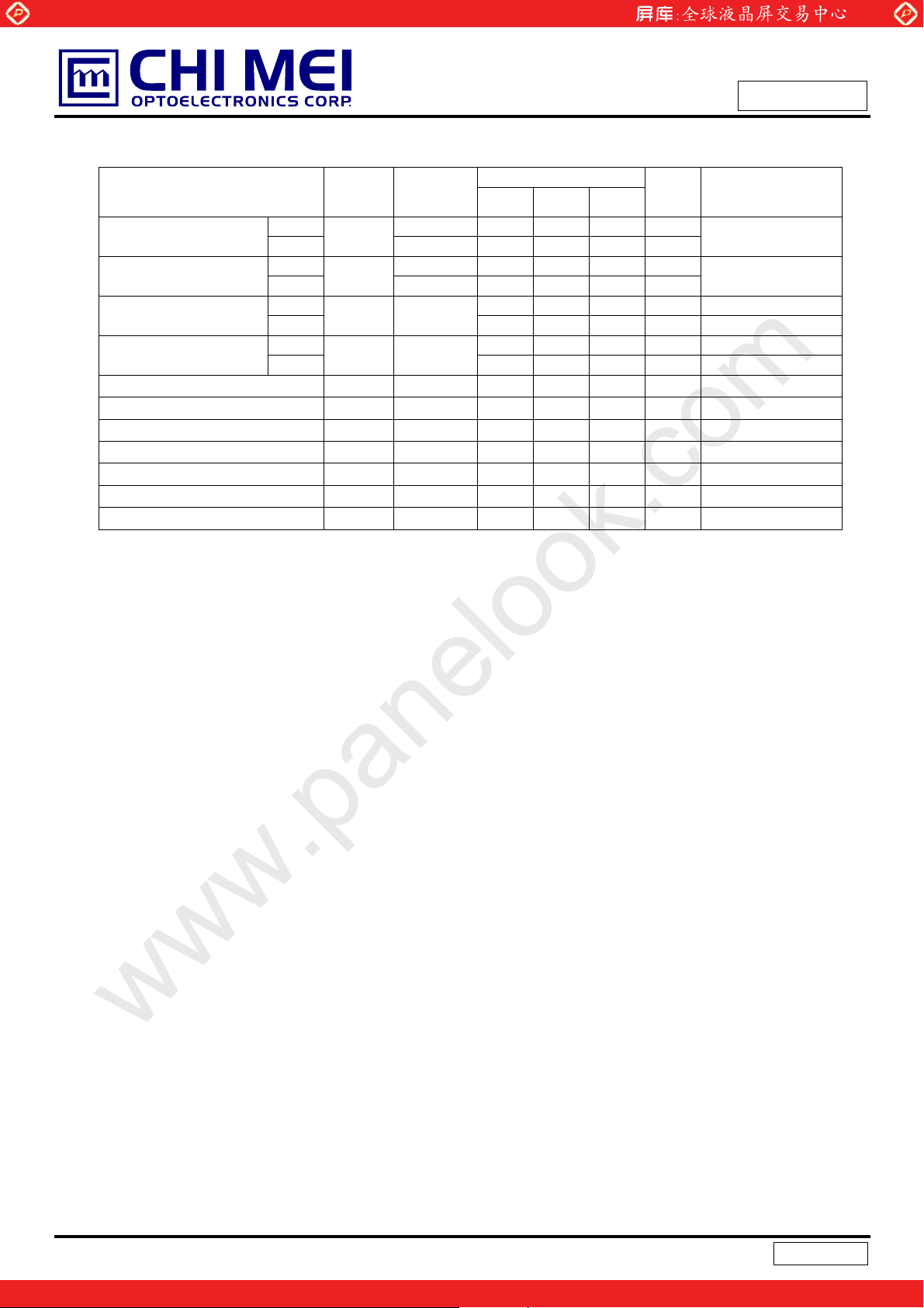
2. ABSOLUTE MAXIMUM RATING
2.1 ABSOLUTE RATINGS OF ENVIRONMENT
Item Symbol
Storage Temperature T
Operating Ambient Temperature T
Shock (Non-Operating) S
Vibration (Non-Operating) V
Note (1) Temperature and relative humidity range is shown in the figure below.
(a) 90 %RH Max. (Ta Љ 40 ºC).
(b) Wet-bulb temperature should be 39 ºC Max. (Ta > 40 ºC).
(c) No condensation.
www.panelook.com
Issued Date: April. 18, 2006
Model No.: V562D1-L01
Value
Min. Max.
ST
OP
X, Y axis - 30 G (3), (5)
NOP
Z axis - 30 G (3), (5)
NOP
-20 +55 ºC (1)
0 40 ºC (1), (2)
- 1.0 G (4), (5)
Unit Note
Preliminary
Note (2) The maximum operating temperature is based on the test condition that the surface temperature of
display area is less than or equal to 65 ºC with LCD module alone in a temperature controlled chamber.
Thermal management should be considered in your product design to prevent the surface temperature
of display area from being over 65 ºC. The range of operating temperature may degrade in case of
improper thermal management in your product design.
Note (3) 11 ms, half sine wave, 1 time for ± X, ± Y, and ± Z.
Note (4) 10 ~ 200 Hz, 10 min, 1 time each X, Y, Z.
Note (5) At testing Vibration and Shock, the fixture in holding the module has to be hard and rigid enough so that
the module would not be twisted or bent by the fixture. The module would not be twisted or bent by the
fixture.
10
5
Version1.0
One step solution for LCD / PDP / OLED panel application: Datasheet, inventory and accessory!
www.panelook.com
Page 6
Global LCD Panel Exchange Center
3. ELECTRICAL MAXIMUM RATINGS
3.1 TFT LCD MODULE
www.panelook.com
Issued Date: April. 18, 2006
Model No.: V562D1-L01
Preliminary
Item Symbol
Value
Unit Note
Min. Max.
Power Supply Voltage
DVI Termination Supply Voltage
DVI Signal Voltage on any pin
DVI Differential Mode Signal
Voltage on any pin
V
CC1
V
CC2
AVcc
-
-
-0.3 20
-0.3 6
4.0
-0.5 4.0
-0.5 4.0
V
V
V
V
(2)
V
Note: (1) Permanent damage to the device may occur if maximum values are exceeded. Function operation
should be restricted to the conditions described under normal operating conditions.
(2) The maximum ratings of the DVI interface are specified in the DVI interface specification of DDWG.
3.2 BACKLIGHT UNIT
Item Symbol
Lamp Voltage V
Power Supply Voltage V
Control Signal Level
W
BL
Ё
Note (1) Permanent damage to the device may occur if maximum values are exceeded. Function operation
should be restricted to the conditions described under Normal Operating Conditions.
Valu e
Min. Max.
Ё
5000 V
Unit Note
RMS
0 30 V (1)
-0.3 7 V (2), (3)
Note (2) No moisture condensation or freezing.
Note (3) The control signals includes On/Off Control, Internal PWM Control, External PWM Control and
Internal/External PWM Selection.
6
Version1.0
One step solution for LCD / PDP / OLED panel application: Datasheet, inventory and accessory!
www.panelook.com
Page 7
Global LCD Panel Exchange Center
www.panelook.com
Issued Date: April. 18, 2006
Model No.: V562D1-L01
4. ELECTRICAL CHARACTERISTICS
4.1 TFT LCD MODULE Ta = 25 ± 2 ºC
Parameter Symbol
V
Power Supply Voltage
Power Supply Ripple Voltage V
Rush Current
White - 2 2.6 A
Black - 1 - A
Power Supply Current
DVI
Interface
Note: (1) The module should be always operated within the above ranges.
Differential Input High Voltage V
Differential Input Low Voltage V
Common Input Voltage V
Reciver Resistor R
Vertical Stripe
White - 2.6 - A
Black - 2.6 - A
Vertical Stripe
CC1
V
CC2
RP1,VRP2
I
RUSH1
I
RUSH2
I
CC1
I
CC2
LVT H
LVT L
LVC
T
Min. Typ. Max.
16.2 18 19.8 V
4.5 5 5.5 V
- - 200 mV
- - 4.5 A
- - 5.0 A
- 1.8 - A
- 3 3.5 A
+150 - +1200 mV
-150 - -1200 mV
0.15 - 1.56 V
95 100 105 ohm
Value
Unit Note
Preliminary
(1)
(3)
(2)
(2)The electrical characteristics of the DVI interface are specified in the DVI interface specification of
DDWG.
(3)The specified power supply current is under the conditions at Vcc1 = 18 V, Vcc2 = 5 V, Ta = 25 ± 2 ºC,
f
= 60 Hz, whereas a power dissipation check pattern below is displayed.
v
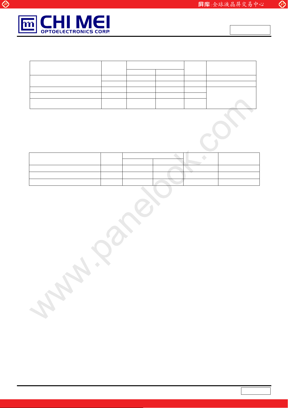
a. White Pattern
Active Area
c. Vertical Stripe Pattern
b. Black Pattern
Active Area
R
G
B
R
G
B
Active Area
R
B
R
B
R R
G
G
G
B
B
B
R
R
G
G
G
B
B
B
7
Version1.0
One step solution for LCD / PDP / OLED panel application: Datasheet, inventory and accessory!
R
R
www.panelook.com
Page 8
Global LCD Panel Exchange Center
4.2 BACKLIGHT UNIT
4.2.1 CCFL (Cold Cathode Fluorescent Lamp) CHARACTERISTICS (Ta=252к)
Parameter Symbol
Lamp Voltage V
Lamp Current I
Lamp Starting Voltage V
Operating Frequency F
Lamp Life Time L
4.2.2 INVERTER CHARACTERISTICS (Ta=252к)
Parameter Symbol
Power Consumption P
Power Supply Voltage V
Power Supply Current I
Input Ripple Noise - - - 500 mV
Backlight Turn on
Voltage
Oscillating Frequency F
Dimming frequency F
Minimum Duty Ratio D
W
L
S
o
BL
www.panelook.com
Value
Min. Typ. Max.
- 1720 -
- 6.5 - mA
- - 2550
- - 2350
40 60 80 KHz (3)
- 50000 - Hrs (4)
Valu e
Min. Typ. Max.
BL
BL
BL
V
BS
W
B 150 160 170 Hz
B
MIN
- 360 378 W (5), IL = 6.5mA
22.8 24.0 25.2 V
- 15 - A Non Dimming
2550 - 2350
--V
47 50 53 kHz
-20-%
Issued Date: April. 18, 2006
Model No.: V562D1-L01
Preliminary
Unit Note
V
RMS
RMS
V
RMS
V
RMS
Unit Note
DC
V
RMS
RMS
IL =6.5mA
(2), Ta = 0 ºC
(2), Ta = 25 ºC
P-P
(1)
VBL=22.8V
Ta = 0 ºC
Ta = 25 ºC
Note (1) Lamp current is measured by utilizing high frequency current meters as shown below:
Note (2) The lamp starting voltage V
should be applied to the lamp for more than 1 second after startup.
S
Otherwise the lamp may not be turned on.
Note (3) The lamp frequency may produce interference with horizontal synchronous frequency of the
display input signals, and it may result in line flow on the display. In order to avoid interference, the
lamp frequency should be detached from the horizontal synchronous frequency and its harmonics
as far as possible.
Note (4) The life time of a lamp is defined as when the brightness is larger than 50% of its original value and
the effective discharge length is longer than 80% of its original length (Effective discharge length is
defined as an area that has equal to or more than 70% brightness compared to the brightness at
the center point of lamp.) as the time in which it continues to operate under the condition at Ta = 25
2к and I
= 6.0 ~ 7.0 mArms.
L
Note (5) The measurement condition of Max. value is based on 56" backlight unit under input voltage 24V,
average lamp current 6.8 mA and lighting 30 minutes later.
8
Version1.0
One step solution for LCD / PDP / OLED panel application: Datasheet, inventory and accessory!
www.panelook.com
Page 9
Global LCD Panel Exchange Center
www.panelook.com
Issued Date: April. 18, 2006
Model No.: V562D1-L01
Preliminary
Inverter
(Master)
a
1
2
a
a
1
2
a
a
1
2
a
a
1
2
a
a
1
2
a
a
1
2
a
a
1
2
a
a
1
2
a
HV (White -)
HV(Blue -)
HV (White +)
HV(Blue +)
HV (White -)
HV(Blue -)
HV (White +)
HV(Blue +)
HV (White -)
HV(Blue -)
HV (White +)
HV(Blue +)
HV (White -)
HV(Blue -)
HV (White +)
HV(Blue +)
A
A
A
A
A
A
A
A
A
A
A
A
A
A
A
A
HV (Pink +)
HV (White +)
HV (Pink -)
HV (White -)
HV (Pink +)
HV (White +)
HV (Pink -)
HV (White -)
HV (Pink +)
HV (White +)
HV (Pink -)
HV (White -)
HV (Pink +)
HV (White +)
HV (Pink -)
HV (White -)
A
b
1
2
A
b
1
A
b
2
A
b
1
A
b
2
A
b
A
b
1
2
A
b
A
b
1
A
b
2
A
b
1
A
b
2
1
A
b
2
A
b
A
b
1
2
A
b
Inverter
(Slave 2)
Inverter
(Slave 1)
LCD Module
a
1
2
a
1
a
2
a
1
a
2
a
a
1
2
a
a
1
2
a
a
1
2
a
a
1
2
a
1
a
2
a
HV (White -)
HV(Blue -)
HV (White +)
HV(Blue +)
HV (White -)
HV(Blue -)
HV (White +)
HV(Blue +)
HV (White -)
HV(Blue -)
HV (White +)
HV(Blue +)
HV (White -)
HV(Blue -)
HV (White +)
HV(Blue +)
A
A
A
A
A
A
A
A
A
A
A
A
A
A
A
A
HV (Pink +)
HV (White +)
HV (Pink -)
HV (White -)
HV (Pink +)
HV (White +)
HV (Pink -)
HV (White -)
HV (Pink +)
HV (White +)
HV (Pink -)
HV (White -)
HV (Pink +)
HV (White +)
HV (Pink -)
HV (White -)
A
b
1
A
b
2
A
b
1
2
A
b
A
b
1
2
A
b
A
b
1
A
b
2
A
b
1
A
b
2
A
b
1
A
b
2
A
b
1
A
b
2
A
b
1
2
A
b
Inverter
(Slave 3)
9
Version1.0
One step solution for LCD / PDP / OLED panel application: Datasheet, inventory and accessory!
www.panelook.com
Page 10
Global LCD Panel Exchange Center
y
y
4.2.3 INVERTER INTERTFACE CHARACTERISTICS
Parameter Symbol
On/Off Control Voltage
Select Voltage
Voltage
Voltage
Control Signal Rising Time Tr
Control Signal Falling Time Tf
PWM Signal Rising Time T
PWM Signal Falling Time T
Input impedance R
BLON Delay Time T
BLON Off Time T
ON
OFF
HI
LO
MAX
MIN
HI 2.0
LO
V
V
V
V
www.panelook.com
Te st
Condition
BLON
SEL
IPWM
EPWM
PWMR
PWMF
IN
on
off
Ё
Ё
Ё
Ё
V
= L
SEL
V
= H
SEL
ЁЁЁ
ЁЁЁ
ЁЁЁ
ЁЁЁ
Ё
Ё 1 ЁЁms
Ё 1 ЁЁms
Valu e
Min. Typ. Max.
2.0
0
2.0
0
Ё
Ё
Ё-
Ё
ЁЁ
Ё
0
Ё
0
Ё
5.0 V
0.8 V
5.0 V Internal/External PWM
0.8 V
3.0 V maximum duty ratioInternal PWM Control
Ё
5.0 V duty on External PWM Control
0.8 V dut
100 ms
100 ms
50 us
50 us
1
ЁЁMӨ
Issued Date: April. 18, 2006
Model No.: V562D1-L01
Preliminary
Unit Note
V minimum dut
off
ratio
Note (1) The SEL signal should be valid before backlight turns on by BLON signal. It is inhibited to change
the internal/external PWM selection (SEL) during backlight turn on period.
Note (2) The power sequence and control signal timing are shown in the following figure.
Note (3) The power sequence and control signal timing must follow the figure below. For a certain reason,
the inverter has a possibility to be damaged with wrong power sequence and control signal timing.
10
Version1.0
One step solution for LCD / PDP / OLED panel application: Datasheet, inventory and accessory!
www.panelook.com
Page 11

Global LCD Panel Exchange Center
BL
V
www.panelook.com
Issued Date: April. 18, 2006
Model No.: V562D1-L01
Preliminary
V
V
V
BLON
V
SEL
EPWM
IPWM
V
0
on1
T
T
off1
2.0V
0
0.8V
Backlight on duration
r
T
T
f
2.0V
0
0.8V
Ext. Dimming Function
T
T
PWMR
PWMF
Int. Dimming Function
2.0V
0
0.8V
3.0V
0
W
External
PWM
Period
External
PWM Duty
100%
Minimun
Duty
11
Version1.0
One step solution for LCD / PDP / OLED panel application: Datasheet, inventory and accessory!
www.panelook.com
Page 12

Global LCD Panel Exchange Center
)
(
)
)
(
)
)
5. BLOCK DIAGRAM
5.1 TFT LCD MODULE
1_Data0(+/-)
1_Data1(+/-)
1_Data2(+/-)
1_Data3(+/-)
1_Data4(+/-)
1_Data5(+/-)
1_Clock(+/-)
2_Data0(+/-)
2_Data1(+/-)
2_Data2(+/-)
2_Data3(+/-)
2_Data4(+/-)
2_Data5(+/-)
2_Clock(+/-)
(74320-1004
Molex
(74320-1004
Molex
CONNECTOR
INPUT
CONNECTOR
INPUT
www.panelook.com
FRAME
BUFFER
TIMING
CONTROLLER
DATA DRIVER (RSDS)
SCAN DRIVER
DATA DRIVER (RSDS
Issued Date: April. 18, 2006
Model No.: V562D1-L01
Preliminary
SCAN DRIVER
TFT LCD PANEL
(3840x3x2160)
Vcc1
Vcc2
GND
VBL
GND
.
SEL
E_PWM
I_PWM
BLON
VBL
GND
GND
POWER
CONNECTOR
(LM113P-020-
TF1-3 (UNE))
CN1.
INVERTER
CONNECTOR
CN1:S14B-PH-SM3-TB
(D)(LF) or equivalent
(Master)
CN4,CN6: 53261-1060(Molex) or equivalent
CN2.
INVERTER
CONNECTOR
CN1:S12B-PH-SM3-TB
(D)(LF) or equivalent
(Slave)
DC/DC CONVERTER
& REFERENCE
VOLTAGE
GENERATOR
CN3,CN5: 53261-1060(Molex) or equivalent
CN8-CN23:SM02 (12.0)B-BHS-1-TB(LF)(JST)
or equivalent
BACKLIGHT
UNIT
INVERTER
CONNECTOR
CN2:S12B-PH-SM3-TB
(D)(LF) or equivalent
(Slave)
INVERTER
CONNECTOR
CN2:S12B-PH-SM3-TB
(D)(LF) or equivalent
(Slave)
CN2.
VBL
GND
VBL
GND
CN5,CN7: 53261-1060(Molex) or equivalent
12
One step solution for LCD / PDP / OLED panel application: Datasheet, inventory and accessory!
Version1.0
www.panelook.com
Page 13

Global LCD Panel Exchange Center
y
y
y
y
y
y
y
y
www.panelook.com
6. LCD INPUT TERMINAL PIN ASSIGNMENT
6.1 TFT LCD MODULE DVI input
CN6, CN7 Connector Pin Assignment
Pin Signal Assignment Pin Signal Assignment Pin Signal Assignment
1 T.M.D.S Data2- 9 T.M.D.S Data1- 17 T.M.D.S Data0-
2 T.M.D.S Data2+ 10 T.M.D.S Data1+ 18 T.M.D.S Data0+
3 T.M.D.S Data2/4 shield 11 T.M.D.S Data1/3 shield 19 T.M.D.S Data0/5 shield
4 T.M.D.S Data4- 12 T.M.D.S Data3- 20 T.M.D.S Data5-
5 T.M.D.S Data4+ 13 T.M.D.S Data3+ 21 T.M.D.S Data5+
6 DDC Clock 14 +5V Power 22 T.M.D.S Clock shield
7 DDC Data 15 Ground(for +5V) 23 T.M.D.S Clock+
Issued Date: April. 18, 2006
Model No.: V562D1-L01
Preliminary
8 No Connect 16 Hot Plug Detect 24 T.M.D.S Clock-
Note: CN6, CN7 Connector part no.: 74320-1004 (Molex) or equivalent.
6.2 TFT LCD MODULE Power input
CN9 Connector Pin Assignment
Pin No. S
1 VIN +18.0Vpower suppl
2 VIN +18.0Vpower suppl
3 VIN +18.0Vpower suppl
4 V5VC +5.0V power suppl
5 V5VC +5.0V power suppl
6 V5VC +5.0V power suppl
7 V5VC +5.0V power suppl
8 GND Ground
9 GND Ground
10 GND Ground
11 GND Ground
12 GND Ground
13 GND Ground
14 GND Ground
15 NC Not connection
16 NC Not connection
17 NC Not connection
18 NC Not connection
19 NC Not connection
20 NC Not connection
mbol Description Note
(1)
Note: (1) CN9 Connector part no.: LM113P-020-TF1-3,UNE(᧵ᤕڠ) or equivalent.
(2) CN10 approve for CMO
13
Version1.0
One step solution for LCD / PDP / OLED panel application: Datasheet, inventory and accessory!
www.panelook.com
Page 14

Global LCD Panel Exchange Center
6.3 BACKLIGHT UNIT
The pin configuration for the housing and the leader wire is shown in the table below.
Pin Name Description Wire Color
1 HV High Voltage Pink
2 HV High Voltage White
Note (1) The backlight interface housing for high voltage side is a model BHR-04VS-1, manufactured by JST.
www.panelook.com
Issued Date: April. 18, 2006
Model No.: V562D1-L01
Preliminary
CN8-CN23: BHR-04VS-1 (JST).
1 HV(White)
2 HV(Pink)
1 HV(White)
2 HV(Pink)
1 HV(White)
2 HV(Pink)
The mating header on inverter part number is SM02(12.0)B-BHS-1-TB(LF).
1 HV(Pink)
2 HV(White)
1 HV(Pink)
2 HV(White)
1 HV(Pink)
2 HV(White)
1
Ϥ
2
Ϥ
31
Ϥ
32
Ϥ
14
Version1.0
One step solution for LCD / PDP / OLED panel application: Datasheet, inventory and accessory!
www.panelook.com
Page 15

Global LCD Panel Exchange Center
6.4 INVERTER UNIT
CN1(Master, Header): S14B-PH-SM3-TB(D)(LF)(JST) or equivalent
Pin No. Symbol Description
1
2
3
4
5
6
7
8
9
10
11
12 E_PWM
13 I_PWM
14 BLON Backlight on/off control
VBL +24V
GND GND
Internal/external PWM selection
SEL
High : external dimming
Low : internal dimming
External PWM control signal
E_PWM should be connected to ground when internal PWM was selected
(SEL = Low).
Internal PWM Control Signal
I_PWM should be connected to ground when external PWM was selected
(SEL = High).
power input
DC
www.panelook.com
Issued Date: April. 18, 2006
Model No.: V562D1-L01
Preliminary
CN2(Slave, Header): S12B-PH-SM3-TB(D)(LF)(JST) or equivalent
Pin No. Symbol Description
1
2
3
4
5
6
7
8
9
10
11
12 NC NC
CN8-CN15(Master, Header), CN16-CN23(Slave, Header): SM02(12.0)B-BHS-1-TB(LF)(JST) or equivalent
Pin No. Symbol Description
1
2
VBL +24V
GND GND
NC NC
CCFL HOT
CCFL HOT
CCFL high voltage
CCFL high voltage
power input
DC
15
Version1.0
One step solution for LCD / PDP / OLED panel application: Datasheet, inventory and accessory!
www.panelook.com
Page 16

Global LCD Panel Exchange Center
CN3-CN4(Master, Header),CN5-CN7(Slaver, Header): 53261-1060(Molex) or equivalent
Pin No. Symbol Description
1 Board to Board
2
3
4
5
6
7
8
9
10
Note (1) Floating of any control signal is not allowed.
Control
Signal
Board to Board
Board to Board
Board to Board
Board to Board
Board to Board
Board to Board
Board to Board
Board to Board
Board to Board
www.panelook.com
Issued Date: April. 18, 2006
Model No.: V562D1-L01
Preliminary
16
Version1.0
One step solution for LCD / PDP / OLED panel application: Datasheet, inventory and accessory!
www.panelook.com
Page 17

Global LCD Panel Exchange Center
6.5 BLOCK DIAGRAM OF INTERFACE
The video picture (3840x2160) should be to divide to two parts : the left side(1920x2160) and the right
side(1920x2160). Each pattern should be send through the dual-DVI interface and the protocol specified in the
DVI interface specification of DDWG.
www.panelook.com
Issued Date: April. 18, 2006
Model No.: V562D1-L01
Preliminary
17
Version1.0
One step solution for LCD / PDP / OLED panel application: Datasheet, inventory and accessory!
www.panelook.com
Page 18

Global LCD Panel Exchange Center
6.6 DVI INTERFACE
Signal Name Signal Description
T.M.D.S. Signals
T.M.D.S. Clock + & - T.M.D.S. clock differential pair.
T.M.D.S. Clock Shield Shield for T.M.D.S. clock differential pair.
T.M.D.S. Data0 + & - T.M.D.S. link #0 channel #0 differential pair.
T.M.D.S. Data0/5 Shield Shared shield for T.M.D.S. link #0 channel #0 and link #1 channel #2.
T.M.D.S. Data1 + & - T.M.D.S. link #0 channel #1 differential pair.
T.M.D.S. Data2/4 Shield Shared shield for T.M.D.S. link #0 channel #2 and link #1 channel #1.
T.M.D.S. Data2 + & - T.M.D.S. link #0 channel #2 differential pair.
www.panelook.com
Issued Date: April. 18, 2006
Model No.: V562D1-L01
Preliminary
T.M.D.S. Data1/3 Shield Shared shield for T.M.D.S. link #0 channel #1 and link #1 channel #0.
T.M.D.S. Data3 + & - T.M.D.S. link #1 channel #0 differential pair.
T.M.D.S. Data4 + & - T.M.D.S. link #1 channel #1 differential pair.
T.M.D.S. Data5 + & - T.M.D.S. link #1 channel #2 differential pair.
Control Signals
Hot Plug Detect(HPD) Signal is driven by monitor to enable the system to identify the
presence of a monitor.
DDC Data The data line for the DDC interface.
DDC Clock The clock line for the DDC interface
+5V Power +5 volt signal provided by the system to enable the monitor to provide
EDID data when the monitor circuitry is not powered.
Ground (for +5V) Ground reference for +5 volt power pin. Used as return by Hsync and
Vsync Signals.
Analog Signals
Analog Red Analog Red signal.
Analog Green Analog Green signal.
Analog Blue Analog Blue signal.
Analog Horizontal Sync Horizontal synchronization signal for the analog interface.
Analog Vertical Sync Vertical synchronization signal for the analog interface.
Analog Ground Common ground for analog signals. Used as a return for analog red,
green and blue signals only.
18
Version1.0
One step solution for LCD / PDP / OLED panel application: Datasheet, inventory and accessory!
www.panelook.com
Page 19

Global LCD Panel Exchange Center
6.7 DVI INTERFACE LINK TIMMING
www.panelook.com
Issued Date: April. 18, 2006
Model No.: V562D1-L01
Preliminary
˜ʳ
˦˸˴
˧ˁˠˁ˗ˁ˦ˁʳ
˟˼˾
˗˘
˗˴˴ʳ˃
˗˴˴ʳ˄
˗˴˴ʳ˅
˴˶˼˸ʳ˼˷˸ʳ˸˺˼ ˴˶˼˸ʳ˼˷˸ʳ˸˺˼
˕˟˨ˮˊˍ˃˰
˺˸˷ ˺˸˷
˚˥ˡˮˊˍ˃˰
˥˘˗ˮˊˍ˃˰
˺˸˷
˸˶˷˸˷ʳ˕˟˨
˸˶˷˸˷ʳ˚˥ˡ
˸˶˷˸˷ʳ˥˘˗
˼˴˶˼˸˂˵˿˴˷ʳ˸˺˼
t
B
˺˸˷
˛˦ˬˡ˖ʿ˩˦ˬˡ˖
˺˸˷
˖˧˟˃ʿ˖˧˟˄
˺˸˷
˖˧˟˅ʿ˖˧˟ˆ
t
E
˸˶˷˸˷ʳ˛˦ˬˡ˖ʿ˩˦ˬˡ˖
˸˶˷˸˷ʳ˖˧˟˃ʿ˖˧˟˄
˸˶˷˸˷ʳ˖˧˟˃ʿ˖˧˟˄
t
E
˕˟˨ˮˊˍ˃˰
˚˥ˡˮˊˍ˃˰
˺˸˷˺˸˷
˥˘˗ˮˊˍ˃˰
˺˸˷
t
E
˸˶˷˸˷ʳ˕˟˨
˸˶˷˸˷ʳ˚˥ˡ
˸˶˷˸˷ʳ˥˘˗
t
E
t
B
˴˶˼˸ʳ˼˷˸ʳ˸˺˼
˥˸˶˸˸˷ʳ
˦˸˴
˗˘
˕˟˨ˮˊˍ˃˰
˶˴ʳ˛˦ˬˡ˖ʿ˩˦ˬˡ˖ ˶˴ʳ˛˦ˬˡ˖ʿ˩˦ˬˡ˖
˚˥ˡˮˊˍ˃˰
˥˘˗ˮˊˍ˃˰
˶˴ʳ˖˧˟˅ʿ˖˧˟ˆ
˼˴˿˼˷
˛˦ˬˡ˖ʿ˩˦ˬˡ˖
˼˴˿˼˷
˖˧˟˃ʿ˖˧˟˄
˼˴˿˼˷
˖˧˟˅ʿ˖˧˟ˆ
˕˟˨ˮˊˍ˃˰
˚˥ˡˮˊˍ˃˰
˶˴ʳ˖˧˟˃ʿ˖˧˟˄˶˴ʳ˖˧˟˃ʿ˖˧˟˄
˥˘˗ˮˊˍ˃˰
˶˴ʳ˖˧˟˅ʿ˖˧˟ˆ
Symbol Description Value Unit
t
Minimum duration blanking period required to ensure character
B
boundary recovery at the receiver. Blanking periods of this
128
T
pixel
duration must occur at least once every 50mS (20Hz).
t
t
Maximum encoding/serializer pipeline delay. 64
E
Maximum recovery/de-serizlizer pipeline delay. Recovery timing
R
includes inter-channel skew, and is measured from the earliest
64
T
pixel
T
pixel
DE transition among the data channels.
19
Version1.0
One step solution for LCD / PDP / OLED panel application: Datasheet, inventory and accessory!
www.panelook.com
Page 20

Global LCD Panel Exchange Center
g
y
(
)
(
)
(
)
)
y
(4)8(
)
(
)
)
y
(
)
(
)
7. INTERFACE TIMING
7.1 INPUT SIGNAL TIMING SPECIFICATIONS
The input signal timing specifications are shown as the following table and timing diagram.
nal Item Symbol Min. Typ. Max. Unit Note
Si
DVI Receiver Clock Frequenc
Frame Rate Fr6 47 50 53 Hz
Vertical Active Display Term
Horizontal Active Display Term
Note: (1) Since this module is operated in DE only mode, Hsync and Vsync input signals should be set to
low logic level. Otherwise, this module would operate abnormally.
Tot a l Tv
Displa
Blank Tvb
Tot a l Th
Displa
Blank Thb
www.panelook.com
1/Tc
Tvd - 2160 - Th
Thd - 3840 - Tc
130
2164
4696
856
152
2168(2320
4700(4900
860
Issued Date: April. 18, 2006
Model No.: V562D1-L01
Preliminary
156
160
1060
MHZ
Th Tv=Tvd+Tvb
Th
Tc Th=Thd+Thb
Tc
˗˘
˚˥ˡˮˊˍ˃˰
˕˟˨˅ˮˊˍ˃˰
˕˟˨ˮˊˍ˃˰
˛˦ˬˡ˖
˩˦ˬˡ˖
˖˧˟˃
˖˧˟˄
˥˘˗ˮˊˍ˃˰
˖˧˟˅
˖˧˟ˆ
˖˟˞
˖˧˟ˇ
˖˧˟ˈ
˧ˁˠˁ˗ˁ˦ˁʳ˴˼˸
˗ˮˊˍ˃˰
˖˃
˖˜
˗˘
˗ˮˊˍ˃˰
˖˃
˖˜
˗˘
˗ˮˊˍ˃˰
˖˃
˖˜
˗˘
˗ˮˊˍ˃˰
˖˃
˖˜
˗˘
˘˶˷˸˂
˦˸˼˴˿˼˸
˘˶˷˸˂
˦˸˼˴˿˼˸
˘˶˷˸˂
˦˸˼˴˿˼˸
˘˶˷˸˂
˦˸˼˴˿˼˸
˗˴˿ʳ˧ˁˠˁ˗ˁ˦ˁʳ˟˼˾
˗˴˴ʳ˃
˗˴˴ʳ˄
˗˴˴ʳ˅
˖˿˶˾
˗˴˴ʳˆ
˧ˁˠˁ˗ˁ˦ˁʳ˸˶˸˼˸
˗ˮˊˍ˃˰
˖˃
˖˜
˗˸˶˷˸
˥˸˶˸˂
˥˸˶˸˂
˥˸˶˸˂
˥˸˶˸˂
˗˘
˗ˮˊˍ˃˰
˖˃
˗˸˶˷˸
˗˘
˗ˮˊˍ˃˰
˖˃
˗˸˶˷˸
˗˘
˗ˮˊˍ˃˰
˖˃
˗˸˶˷˸
˗˘
˖˜
˖˜
˖˜
˕˟˨ˮˊˍ˃˰
˛˦ˬˡ˖
˩˦ˬˡ˖
˗˘˃
˚˥ˡˮˊˍ˃˰
˖˧˟˃
˖˧˟˄
˗˘˄
˥˘˗ˮˊˍ˃˰
˖˧˟˅
˖˧˟ˆ
˗˘˅
˕˟˨˅ˮˊˍ˃˰
˖˧˟ˇ
˖˧˟ˈ
˗˘ˆ
˥˸˶˸˸˷ʳ
˦˸˴
˕˟˨ˮˊˍ˃˰
˛˦ˬˡ˖
˩˦ˬˡ˖
˚˥ˡˮˊˍ˃˰
˖˧˟˃
˖˧˟˄
˥˘˗ˮˊˍ˃˰
˖˧˟˅
˖˧˟ˆ
˖˟˞
˕˟˨˅ˮˊˍ˃˰
˖˧˟ˇ
˖˧˟ˈ
˚˥ˡ˅ˮˊˍ˃˰
˖˧˟ˉ
˖˧˟ˊ
˥˘˗˅ˮˊˍ˃˰
˖˧˟ˋ
˖˧˟ˌ
Notes: The TMDS protocol of DVI interface are specified in the DVI interface specification of DDWG
˗ˮˊˍ˃˰
˖˃
˖˜
˗˘
˗ˮˊˍ˃˰
˖˃
˖˜
˗˘
˗˴˴ʳˇ
˘˶˷˸˂
˦˸˼˴˿˼˸
˗˴˴ʳˈ
˘˶˷˸˂
˦˸˼˴˿˼˸
˗˸˶˷˸
˥˸˶˸˂
˗˸˶˷˸
˥˸˶˸˂
˗ˮˊˍ˃˰
˖˃
˖˜
˗˘
˗ˮˊˍ˃˰
˖˃
˖˜
˗˘
˚˥ˡ˅ˮˊˍ˃˰
˖˧˟ˉ
˖˧˟ˊ
˗˘ˇ
˥˘˗˅ˮˊˍ˃˰
˖˧˟ˋ
˖˧˟ˌ
˗˘ˈ
20
Version1.0
One step solution for LCD / PDP / OLED panel application: Datasheet, inventory and accessory!
˚˥ˡ˅ˮˊˍ˃˰
˖˧˟ˉ
˖˧˟ˊ
˥˘˗˅ˮˊˍ˃˰
˖˧˟ˋ
˖˧˟ˌ
www.panelook.com
Page 21

Global LCD Panel Exchange Center
7.2 POWER ON/OFF SEQUENCE
To prevent a latch-up or DC operation of LCD module, the power on/off sequence should follow the
diagram below.
www.panelook.com
Issued Date: April. 18, 2006
Model No.: V562D1-L01
Preliminary
Note : (1) The supply voltage of the external system for the module input should follow the definition of Vcc.
(2) Apply the lamp voltage within the LCD operation range. When the backlight turns on before the LCD
operation or the LCD turns off before the backlight turns off, the display may momentarily become
abnormal screen.
(3) In case of Vcc is in off level, please keep the level of input signals on the low or high impedance.
(4) T4 should be measured after the module has been fully discharged between power off and on period.
(5) Interface signal shall not be kept at high impedance when the power is on.
21
Version1.0
One step solution for LCD / PDP / OLED panel application: Datasheet, inventory and accessory!
www.panelook.com
Page 22

Global LCD Panel Exchange Center
8. OPTICAL CHARACTERISTICS
8.1 TEST CONDITIONS
Item Symbol Value Unit
Ambient Temperature Ta
Ambient Humidity Ha
Supply Voltage V
Input Signal According to typical value in "3. ELECTRICAL CHARACTERISTICS"
Lamp Current I
Oscillating Frequency (Inverter) F
Frame Rate F
8.2 OPTICAL SPECIFICATIONS
www.panelook.com
CC
L
L
r
Issued Date: April. 18, 2006
Model No.: V562D1-L01
25r2
50r10
5.0 V
6.5r0.5
50r3
60 Hz
Preliminary
o
C
%RH
mA
KHz
The relative measurement methods of optical characteristics are shown in 7.2. The following items should be
measured under the test conditions described in 7.1 and stable environment shown in Note (6).
Item Symbol Condition Min. Typ. Max. Unit Note
Contrast Ratio CR (1200) - Note (2)
Gray to
Response Time
(6.5) ms Note (3)
gray
Center Luminance of White L
Average Luminance of White
White Variation
L
GW
C
AVE
(500) cd/m2Note (4)
(450) - cd/m2Note (4)
(1.6) - Note (7)
Cross Talk CT (4) % Note (5)
T
=0q, TY =0q
x
Viewing Normal Angle
Typ.
-0.03
(0.332)
(0.275)
(0.601)
(0.142)
(0.065)
Typ.
+0.03
-
-
Note (6)
-
-
Color
Chromaticity
Red
Rx (0.652) -
Ry
Gx
Green
Gy
Bx
Blue
By
Wx
0.285
White
Wy
Color Gamut C.G
Tx+
(72) 75 % NTSC
(80) (88)
0.293
Horizontal
Viewing
Angle
T
x
TY+
CRt30
(80) (88)
(80) (88)
Vertical
T
-
Y
(80) (88)
22
Version1.0
One step solution for LCD / PDP / OLED panel application: Datasheet, inventory and accessory!
-
-
Deg. Note (1)
www.panelook.com
Page 23

Global LCD Panel Exchange Center
Note (1) Definition of Viewing Angle (Tx, Ty):
Viewing angles are measured by Eldim EZ-Contrast 160R
www.panelook.com
Issued Date: April. 18, 2006
Model No.: V562D1-L01
Preliminary
Normal
Tx = Ty = 0º
Ty- Ty
TX- = 90º
6 o’clock
T
y- = 90º
x-
y-
Note (2) Definition of Contrast Ratio (CR):
The contrast ratio can be calculated by the following expression.
Contrast Ratio (CR) = L255 / L0
L255: Luminance of gray level 255
L 0: Luminance of gray level 0
CR = CR (5), where CR (X) is corresponding to the Contrast Ratio of the point X at the figure in Note
(7).
Tx
Tx
12 o’clock direction
y+
T
y+ = 90º
x+
TX+ = 90º
Note (3) Definition of Gray to Gray Switching Time:
100%
90%
Optical
Response
10%
0%
Gray to gray
switching time
The driving signal means the signal of gray level 0, 63, 127, 191, 255.
Gray to gray average time means the average switching time of gray level 0 ,63,127,191,255 to each
other.
Time
Time
Gray to gray
switching time
23
Version1.0
One step solution for LCD / PDP / OLED panel application: Datasheet, inventory and accessory!
www.panelook.com
Page 24

Global LCD Panel Exchange Center
A
A
www.panelook.com
Issued Date: April. 18, 2006
Model No.: V562D1-L01
Preliminary
Note (4) Definition of Luminance of White (LC, L
Measure the luminance of gray level 255 at center point and 5 points
L
= L (5)
C
L
= [L (1)+ L (2)+ L (3)+ L (4)+ L (5)] / 5
AVE
Where L (x) is corresponding to the luminance of the point X at the figure in Note (7).
Note (5) Definition of Cross Talk (CT):
CT = | Y
– YB
| / YAu 100 (%)
B
A
Where:
Y
= Luminance of measured location without gray level 0 pattern (cd/m2)
A
Y
= Luminance of measured location with gray level 0 pattern (cd/m )B
B
ctive Area
Gray 128
Y
A, U
Y
A, R
(D,W)
(D/2,W/8)
(7D/8,W/2)
Y
(D/8,W/2)
A, L
(D/2,7W/8)
Y
A, D
(0, 0)
AVE
):
2
ctive Area
Gray 0
Gray 0
Gray 128
Y
B, U
Y
B, R
(3D/4,3W/4)
(D,W)
(D/2,W/8)
(7D/8,W/2)
(D/4,W/4)
Y
(D/8,W/2)
B, L
Y
(D/2,7W/8)
B, D
(0, 0)
24
Version1.0
One step solution for LCD / PDP / OLED panel application: Datasheet, inventory and accessory!
www.panelook.com
Page 25

Global LCD Panel Exchange Center
Note (6) Measurement Setup:
The LCD module should be stabilized at given temperature for 1 hour to avoid abrupt
temperature change during measuring. In order to stabilize the luminance, the measurement
should be executed after lighting backlight for 1 hour in a windless room.
LCD Module
LCD Panel
www.panelook.com
Issued Date: April. 18, 2006
Model No.: V562D1-L01
Preliminary
Center of the Screen
Note (7) Definition of White Variation (GW):
Measure the luminance of gray level 255 at 5 points
GW = Maximum [L (1), L (2), L (3), L (4),ΕΕΕ, L (13)] / Minimum [L (1), L (2), L (3), L (4),ΕΕΕ, L (13)]
D/10 9D/10
3D/10 5D/10 7D/10
Display Color Analyzer
(Minolta CA210)
Light Shield Room
(Ambient Luminance < 2 lux)
D
W/10
3W/10
5W/10
W
Vertical Line
7W/10
9W/10
11
1
4
6
9
2
5
7
10
12
13
3
X
8
: Test Point
X=1 to 13
Active Area
25
Version1.0
One step solution for LCD / PDP / OLED panel application: Datasheet, inventory and accessory!
www.panelook.com
Page 26

Global LCD Panel Exchange Center
www.panelook.com
Issued Date: April. 18, 2006
Model No.: V562D1-L01
Preliminary
9. PRECAUTIONS
9.1 ASSEMBLY AND HANDLING PRECAUTIONS
(1) Do not apply rough force such as bending or twisting to the module during assembly.
(2) It is recommended to assemble or to install a module into the user’s system in clean working areas. The
dust and oil may cause electrical short or worsen the polarizer.
(3) Do not apply pressure or impulse to the module to prevent the damage of LCD panel and Backlight.
(4) Always follow the correct power-on sequence when the LCD module is turned on. This can prevent the
damage and latch-up of the CMOS LSI chips.
(5) Do not plug in or pull out the I/F connector while the module is in operation.
(6) Do not disassemble the module.
(7) Use a soft dry cloth without chemicals for cleaning, because the surface of polarizer is very soft and
easily scratched.
(8) Moisture can easily penetrate into LCD module and may cause the damage during operation.
(9) When storing modules as spares for a long time, the following precaution is necessary.
a. Do not leave the module in high temperature, and high humidity for a long time.It is highly
recommended to store the module with temperature from 0 to 35кat normal humidity
without condensation.
b. The module shall be stored in dark place. Do not store the TFT-LCD module in direct
sunlight or fluorescent light.
(10) When ambient temperature is lower than 10ºC, the display quality might be reduced. For example, the
response time will become slow, and the starting voltage of CCFL will be higher than that of room
temperature.
9.2 SAFETY PRECAUTIONS
(1) The startup voltage of a Backlight is approximately 1000 Volts. It may cause an electrical shock while
assembling with the inverter. Do not disassemble the module or insert anything into the Backlight unit.
(2) If the liquid crystal material leaks from the panel, it should be kept away from the eyes or mouth. In case
of contact with hands, skin or clothes, it has to be washed away thoroughly with soap.
(3) After the module’s end of life, it is not harmful in case of normal operation and storage.
9.3 SAFETY STANDARDS
The LCD module should be certified with safety regulations as follows:
(1) UL60950-1 or updated standard.
(2) IEC60950-1 or updated standard.
(3) UL60065 or updated standard.
(4) IEC60065 or updated standard.
26
Version1.0
One step solution for LCD / PDP / OLED panel application: Datasheet, inventory and accessory!
www.panelook.com
Page 27

Global LCD Panel Exchange Center
10. DEFINITION OF LABELS
10.1 CMO MODULE LABEL
The barcode nameplate is pasted on each module as illustration, and its definitions are as following explanation.
CHI MEI
OPTOELECTRONICS
(a) Model Name: V562D1-L01
(b) Revision: Rev. XX, for example: A0, A1… B1, B2… or C1, C2…etc.
www.panelook.com
V562D1 -L01 Rev. XX
X X X X X X X Y M D L N N N N
MADE IN TAIWAN
Issued Date: April. 18, 2006
Model No.: V562D1-L01
Preliminary
E207943
MADE IN TAIWAN
RoHS
(c) Serial ID: X X
Serial ID includes the information as below:
Day: 1~9, A~Y, for 1
X X X X X Y M D L N N N N
(a) Manufactured Date: Year: 0~9, for 2000~2009
Month: 1~9, A~C, for Jan. ~ Dec.
(b) Revision Code: Cover all the change
(c) Serial No.: Manufacturing sequence of product
Serial No.
Product Line
Year, Month, Date
CMO Internal Use
CMO Internal Use
Revision
CMO Internal Use
st
to 31st, exclude I ,O, and U.
(d) Product Line: 1 -> Line1, 2 -> Line 2, …etc.
27
Version1.0
One step solution for LCD / PDP / OLED panel application: Datasheet, inventory and accessory!
www.panelook.com
Page 28

Global LCD Panel Exchange Center
11. PACKAGE
11.1 PACKING SPECIFICATIONS
(1) 2 LCD TV modules / 1 Box
(2) Box dimensions : 1448(L) X 372 (W) X 901 (H)
(3) Weight : approximately 56Kg (2 modules per box)
11.2 PACKING METHOD
Figures 9-1 and 9-2 are the packing method
LCD TV Module
www.panelook.com
Issued Date: April. 18, 2006
Model No.: V562D1-L01
Preliminary
Anti-static Bag
4pcs Drier
Cushion(Bottom)
Carton
Carton Label
4pcs Joint
Figure.9-1 packing method
28
Version1.0
One step solution for LCD / PDP / OLED panel application: Datasheet, inventory and accessory!
www.panelook.com
Page 29

Global LCD Panel Exchange Center
Sea Transportation
Corner Protector:L1780*50mm*50mm
Corner Protector:L1130*50mm*50mm
Pallet:L1150*W1460*H140mm
Pallet Stack:L1150*W1460*H1942mm
Gross:353kg
www.panelook.com
Issued Date: April. 18, 2006
Model No.: V562D1-L01
Preliminary
PP Belt
Figure. 9-2 Packing method
PP Belt
29
Version1.0
One step solution for LCD / PDP / OLED panel application: Datasheet, inventory and accessory!
www.panelook.com
Page 30

Global LCD Panel Exchange Center
12. MECHANICAL CHARACTERISTIC
www.panelook.com
Issued Date: April. 18, 2006
Model No.: V562D1-L01
Preliminary
࡛ભሽٝڶૻֆ
%*+/'+
30
Version1.0
One step solution for LCD / PDP / OLED panel application: Datasheet, inventory and accessory!
www.panelook.com
Page 31

Global LCD Panel Exchange Center
www.panelook.com
Issued Date: April. 18, 2006
Model No.: V562D1-L01
Preliminary
࡛ભሽٝڶૻֆ
%*+/'+
31
Version1.0
One step solution for LCD / PDP / OLED panel application: Datasheet, inventory and accessory!
www.panelook.com
Page 32

Global LCD Panel Exchange Center
www.panelook.com
Issued Date: April. 18, 2006
Model No.: V562D1-L01
Preliminary
࡛ભሽٝڶૻֆ
%*+/'+
32
Version1.0
One step solution for LCD / PDP / OLED panel application: Datasheet, inventory and accessory!
www.panelook.com
 Loading...