

Page 1
Global LCD Panel Exchange Center
TFT LCD Approval Specification
MODEL NO.: V546H1-PH5
Customer: _________________________________
Approved by:_______________________________
www.panelook.com
Issue Date:Jan. 22.2009
Model No.: V546H1-PH5
Approval
Note:
TV Head Division
Approved By
LY C hen
Reviewed By
QA Dept. Product Development Div.
Kc_Ko WT Lin
Prepared By
LCD TV Marketing and Product Management Div.
Wang-Yang Li Trina Lee
1
One step solution for LCD / PDP / OLED panel application: Datasheet, inventory and accessory!
Version 2.0
www.panelook.com
Page 2

Global LCD Panel Exchange Center
www.panelook.com
Issue Date:Jan. 22.2009
Model No.: V546H1-PH5
Approval
CONTENTS
REVISION HISTORY ..................................................................................................................................................4
1. GENERAL DESCRIPTION......................................................................................................................................5
1.1 OVERVIEW....................................................................................................................................................5
1.2 FEATURES ....................................................................................................................................................5
1.3 MECHANICAL SPECIFICATIONS ..................................................................................................................5
2. ABSOLUTE MAXIMUM RATINGS ...........................................................................................................................6
2.1 ABSOLUTE RATINGS OF ENVIRONMENT (BASE ON CMO MODULE V546H1-LH1) ...................................6
2.2 PACKAGE STORAGE....................................................................................................................................7
2.3 ELECTRICAL ABSOLUTE RATINGS..............................................................................................................7
2.3.1 ELECTRICAL ABSOLUTE RATINGS (OPEN CELL) .............................................................................7
3. ELECTRICAL CHARACTERISTICS ........................................................................................................................8
3.1 TFT LCD MODULE.........................................................................................................................................8
3.2 RSDS CHARACTERISTICS ...........................................................................................................................8
4. BLOCK DIAGRAM OF INTERFACE ........................................................................................................................9
4.1 TFT LCD MODULE.........................................................................................................................................9
5. INPUT TERMINAL PIN ASSIGNMENT ..................................................................................................................10
5.1 TFT LCD Module Input .................................................................................................................................10
5.2 BLOCK DIAGRAM OF INTERFACE .............................................................................................................12
5.3 LVDS INTERFACE ....................................................................................................................................... 13
5.4 COLOR DATA INPUT ASSIGNMENT............................................................................................................14
6. INTERFACE TIMING............................................................................................................................................. 15
6.1 INPUT SIGNAL TIMING SPECIFICATIONS(Ta = 25 ± 2 ºC)..........................................................................15
6.2 INTERNAL SIGNAL TIMING SPECIFICATIONS(FRCШT-CON)(Ta = 25 ± 2 ºC) ........................................... 15
6.2 POWER ON/OFF SEQUENCE .....................................................................................................................17
7. OPTICAL CHARACTERISTICS.............................................................................................................................18
7.1 TEST CONDITIONS.....................................................................................................................................18
7.2 OPTICAL SPECIFICATIONS........................................................................................................................18
8. PRECAUTIONS ....................................................................................................................................................21
2
One step solution for LCD / PDP / OLED panel application: Datasheet, inventory and accessory!
Version 2.0
www.panelook.com
Page 3
Global LCD Panel Exchange Center
www.panelook.com
Issue Date:Jan. 22.2009
Model No.: V546H1-PH5
Approval
8.1 ASSEMBLY AND HANDLING PRECAUTIONS .............................................................................................21
8.2 SAFETY PRECAUTIONS .............................................................................................................................21
9. DEFINITION OF LABELS......................................................................................................................................22
9.1 OPEN CELL LABEL .....................................................................................................................................22
9.2 CARTON LABEL .......................................................................................................................................... 22
10. PACKAGING.......................................................................................................................................................23
10.1 PACKAGING SPECIFICATIONS.................................................................................................................23
10.2 PACKAGING METHOD .............................................................................................................................. 23
11. MECHANICAL CHARACTERISTICS ...................................................................................................................25
3
One step solution for LCD / PDP / OLED panel application: Datasheet, inventory and accessory!
Version 2.0
www.panelook.com
Page 4
Global LCD Panel Exchange Center
REVISION HISTORY
Version Date Page(New) Section Description
Ver. 2.0 Jan 22, 2009 All All The Approval specification was first issued.
www.panelook.com
Issue Date:Jan. 22.2009
Model No.: V546H1-PH5
Approval
4
One step solution for LCD / PDP / OLED panel application: Datasheet, inventory and accessory!
Version 2.0
www.panelook.com
Page 5
Global LCD Panel Exchange Center
y
1. GENERAL DESCRIPTION
1.1 OVERVIEW
V546H1-PH5 is a 54.6” TFT Liquid Crystal Display cell with driver ICs and 2ch-LVDS interface. This product
supports 1920 x 1080 Full HDTV format and can display 1.073G colors (10-bit/color). The backlight unit is not
built-in.
1.2 FEATURES
CHARACTERISTICS ITEMS SPECIFICATIONS
Screen Diagonal [in] 54.6
Pixels [lines] 1920ʳ 1080
Active Area [mm] 1209.6(H) x 680.4(V) (54.6” diagonal)
Sub-Pixel Pitch [mm] 0.21(H) x 0.63(V)
Pixel Arrangement RGB vertical stripe
Weight [g] 3392
Physical Size [mm] 1251.4(W) x 737(H) x 1.75(D) Typ
Display Mode Transmissive mode / Normally black
Contrast Ratio 4000:1 Typ.
Glass thickness (Array / CF) [mm] 0.7 / 0.7
Viewing Angle (CR>20) +88/-88(H),+88/-88(V) Typ.
Color Chromaticity R=(0.655, 0.326)
Cell Transparency [%] 5.6%Typ.
Polarizer Surface Treatment Anti-Glare coating (Super Clear)
www.panelook.com
Issue Date:Jan. 22.2009
Model No.: V546H1-PH5
Approval
(Typical value measured at CMO’s module)
(Typical value measured at CMO’s module)
G=(0.299, 0.599)
B=(0.147, 0.099)
W=(0.333, 0.372)
(Light source is the standard light source “C” which is defined b
and driving voltages are based on suitable gamma voltages.)
(Typical value measured at CMO’s module)
Hardness (3H)
CIE
1.3 MECHANICAL SPECIFICATIONS
Item Min. Typ. Max. Unit Note
Weight - 3392 - g -
I/F connector mounting position
Note (1) Please refer to the attached drawings for more information of front and back outline dimensions.
Note (2) Connector mounting position
The mounting inclination of the connector makes the
screen center within
0.5mm as the horizontal.
+/- 0.5mm
5
One step solution for LCD / PDP / OLED panel application: Datasheet, inventory and accessory!
(2)
Version 2.0
www.panelook.com
Page 6
Global LCD Panel Exchange Center
www.panelook.com
2. ABSOLUTE MAXIMUM RATINGS
2.1 ABSOLUTE RATINGS OF ENVIRONMENT (BASE ON CMO MODULE V546H1-LH1)
Value
Item Symbol
Min. Max.
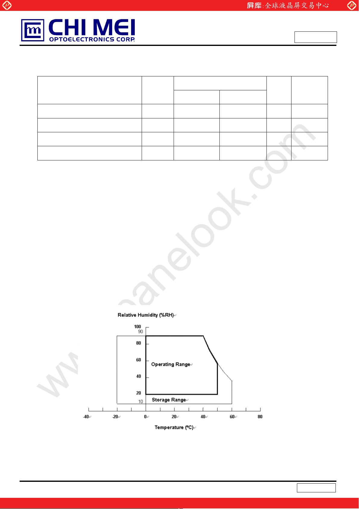
Storage Temperature TST -20 +60 ºC (1)
Operating Ambient Temperature TOP 0 50 ºC (1), (2)
Shock (Non-Operating) SNOP - 50 G (3), (5)
Vibration (Non-Operating) VNOP - 1.0 G (4), (5)
Note (1) Temperature and relative humidity range is shown in the figure below.
Issue Date:Jan. 22.2009
Model No.: V546H1-PH5
Approval
Unit Note
(a) 90 %RH Max. (Ta
(b) Wet-bulb temperature should be 39 ºC Max. (Ta > 40 ºC).
(c) No condensation.
Note (2) The maximum operating temperature is based on the test condition that the surface temperature of
display area is less than or equal to 65 ºC with LCD module alone in a temperature controlled chamber.
Thermal management should be considered in final product design to prevent the surface temperature of
display area from being over 65 ºC. The range of operating temperature may degrade in case of
improper thermal management in final product design.
Note (3) 11 ms, half sine wave, 1 time for ± X, ± Y, ± Z.
Note (4) 10 ~ 200 Hz, 10 min, 1 time each X, Y, Z.
Note (5) At testing Vibration and Shock, the fixture in holding the module has to be hard and rigid enough so that
the module would not be twisted or bent by the fixture.
Љ
40 ºC).
6
One step solution for LCD / PDP / OLED panel application: Datasheet, inventory and accessory!
Version 2.0
www.panelook.com
Page 7
Global LCD Panel Exchange Center
2.2 PACKAGE STORAGE
Storage condition: With shipping package.
www.panelook.com
Issue Date:Jan. 22.2009
Model No.: V546H1-PH5
Approval
Storage temperature rang: 25
Storage humidity range: 50
Shelf life: a month
2.3 ELECTRICAL ABSOLUTE RATINGS
2.3.1 ELECTRICAL ABSOLUTE RATINGS (OPEN CELL)
Item Symbol
Power Supply Voltage VAA -0.3 17.9 V
Power Supply Voltage V
Power Supply Voltage VGL -5.7 -0.3 V
Logic Input Voltage VDD -0.3 3.4 V
Note (1) Permanent damage to the device may occur if maximum values are exceeded. Function operation
should be restricted to the conditions described under Normal Operating Conditions.
5к
10%RH
GHP
Value
Unit Note
Min. Max.
-0.3 32.3 V
(1)
7
One step solution for LCD / PDP / OLED panel application: Datasheet, inventory and accessory!
Version 2.0
www.panelook.com
Page 8
Global LCD Panel Exchange Center
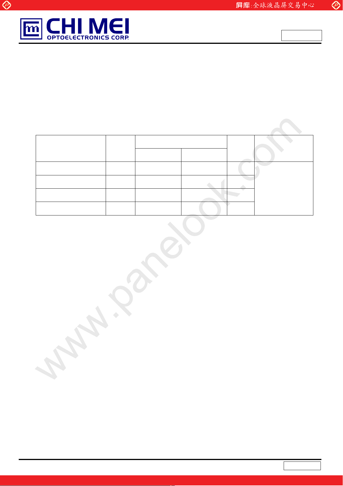
3. ELECTRICAL CHARACTERISTICS
3.1 TFT LCD MODULE
(Ta = 25 ± 2 ºC)
Parameter Symbol
www.panelook.com
Issue Date:Jan. 22.2009
Model No.: V546H1-PH5
Approval
Value
Unit Note
Min. Typ. Max.
31.3 31.8 32.3 V
-5.7 -5.5 -5.3 V
17.5 17.7 17.9 V
3.2 3.3 3.4 V
- - 50 mA
- - 50 A
- - 1300 A
- - 2300 A
Power Supply Voltage
Power Supply Current
CMOS
interface
Input High Threshold Voltage 2.7 3.3 V
Input Low Threshold Voltage 0 0.7 V
VGH
VGL
VAA
V
DD
IGH
IGL
IAA
I
33V
Note (1) The module should be always operated within the above ranges.
3.2 RSDS CHARACTERISTICS
(Ta = -10 ± 85 ºC)
Item Symbol Condition
RSDS high input Voltage V
RSDS low input Voltage V
RSDS common mode input
voltage range
RSDS Input leakage current
Note (1) V
Note (2) V
Note (3) V
= (VCLKP + VCLKN)/2 or V
CMRSDS
DIFFRSDS
CMRSDS
= VCLKP - VCLKN or V
= +1.2V(VDDD = 3.3V)
DIFFRSDSVCMRSDS
DIFFRSDSVCMRSDS
V
CMRSDSVDIFFRSDS
D
I
DL
= +1.2V(1) 100 200 mV
= +1.2V(1) -200 -100 mV
= 200mV
(2)
P, DXXN, CLKO,
XX
VSSD + 0.1 Note(3) VSSD + 1.2 V
CLPN
= (VDXXP + VDXXN)/2
CMRSDS
DIFFRSDS
= VDXXP - VDXXN
Value Unit
Min. Typ. Max.
Ӵ
-10 - 10
A
8
One step solution for LCD / PDP / OLED panel application: Datasheet, inventory and accessory!
Version 2.0
www.panelook.com
Page 9
Global LCD Panel Exchange Center
4. BLOCK DIAGRAM OF INTERFACE
4.1 TFT LCD MODULE
www.panelook.com
Issue Date:Jan. 22.2009
Model No.: V546H1-PH5
Approval
TFT LCD PANEL
(1920x3x1080)
X(R) Board X(L) Board
PPRSDS SIGNAL INPUT
Connector Parts No.: FH31H-80S-0.5SH(06),Hirose connector or
9
One step solution for LCD / PDP / OLED panel application: Datasheet, inventory and accessory!
Version 2.0
www.panelook.com
Page 10

Global LCD Panel Exchange Center
5. INPUT TERMINAL PIN ASSIGNMENT
5.1 TFT LCD Module Input
Pin assignment
www.panelook.com
Issue Date:Jan. 22.2009
Model No.: V546H1-PH5
Approval
CN1(XL) Connector Pin Assignment
Pin No. Symbol Description Pin No. Symbol Description
1 GND Ground 41 AD0M_1
2 BD1P_4
3 BD1M_4
4 GND Ground 44 GM19
5 N.C. No connection 45 GM18
6 N.C. No connection 46 GM17
7 GND Ground 47 GM16
8 BD0P_4
9 BD0M_4
10 AD1P_4
11 AD1M_4
12 AD0P_4
13 AD0M_4
14 BD1P_3
15 BD1M_3
16 BD0P_3
17 BD0M_3
18 AD1P_3
19 AD1M_3
20 AD0P_3
21 AD0M_3
22 BD1P_2
23 BD1M_2
24 BD0P_2
25 BD0M_2
26 AD1P_2
27 AD1M_2
28 GND Ground 68 STV
29 A_CLKP
30 A_CLKM
31 GND Ground 71 VDD
32 AD0P_2
33 AD0M_2
34 BD1P_1
35 BD1M_1
36 BD0P_1
37 BD0M_1
38 AD1P_1
39 AD1M_1
40 AD0P_1
B-Path RSDS data signal
B-Path RSDS data signal
B-Path RSDS data signal
B-Path RSDS data signal
A-Path RSDS data signal
A-Path RSDS data signal
A-Path RSDS data signal
A-Path RSDS data signal
B-Path RSDS data signal
B-Path RSDS data signal
B-Path RSDS data signal
B-Path RSDS data signal
A-Path RSDS data signal
A-Path RSDS data signal
A-Path RSDS data signal
A-Path RSDS data signal
B-Path RSDS data signal
B-Path RSDS data signal
B-Path RSDS data signal
B-Path RSDS data signal
A-Path RSDS data signal
A-Path RSDS data signal
Data driver clock
Data driver clock
A-Path RSDS data signal
A-Path RSDS data signal
B-Path RSDS data signal
B-Path RSDS data signal
B-Path RSDS data signal
B-Path RSDS data signal
A-Path RSDS data signal
A-Path RSDS data signal
A-Path RSDS data signal
A-Path RSDS data signal
42 GND Ground
43 GM20
48 GM15
49 GM14
50 GM13
51 GM12
52 GM11
53 GM10
54 GM9
55 GM8
56 GM7
57 GM6
58 GM5
59 GM4
60 GM3
61 GM2
62 GM1
63 GND Ground
64 TP1
65 CKV
66 OE1
67 OE2 Scan driver output enable 2
69 GND Ground
70 VDD
72 VDDA
73 VDDA
74 VCM VCM Power supply
75 VCM VCM Power supply
76 VGL
77 VGL
78 VGH
79 VGH
80 GND Ground
Gamma Power supply
Gamma Power supply
Gamma Power supply
Gamma Power supply
Gamma Power supply
Gamma Power supply
Gamma Power supply
Gamma Power supply
Gamma Power supply
Gamma Power supply
Gamma Power supply
Gamma Power supply
Gamma Power supply
Gamma Power supply
Gamma Power supply
Gamma Power supply
Gamma Power supply
Gamma Power supply
Gamma Power supply
Gamma Power supply
RSDS data latch
Scan driver clock
Scan driver output enable 1
Scan driver start pulse
Logic Power supply
Logic Power supply
Driver Power supply
Driver Power supply
Driver Power supply
Driver Power supply
Driver Power supply
Driver Power supply
10
One step solution for LCD / PDP / OLED panel application: Datasheet, inventory and accessory!
Version 2.0
www.panelook.com
Page 11

Global LCD Panel Exchange Center
www.panelook.com
Issue Date:Jan. 22.2009
Model No.: V546H1-PH5
Approval
CN2(XR) Connector Pin Assignment
Pin No. Symbol Description Pin No. Symbol Description
1 GND Ground 41 BD1M_6
2 VGH
3 VGH
4 VGL
5 VGL
6 VCM VCM Power supply 46 AD0P_6
7 VCM VCM Power supply 47 AD0M_6
8 VDDA
9 VDDA
10 VDD
11 VDD
12 GND Ground 52 GND Ground
13 VSCM VSCM Power supply 53 GM20
14 TP1
15 STV
16 CKV
17 OE2 Scan driver output enable 2
18 OE1
19 GND Ground 59 GM14
20 BD1P_8
21 BD1M_8
22 BD0P_8
23 BD0M_8
24 AD1P_8
25 AD1M_8
26 AD0P_8
27 AD0M_8
28 GND Ground 68 GM5
29 C_CLKP
30 C_CLKM
31 GND Ground 71 GM2
32 BD1P_7
33 BD1M_7
34 BD0P_7
35 BD0M_7
36 AD1P_7
37 AD1M_7
38 AD0P_7
39 AD0M_7
40 BD1P_6
Note (1) CN1Ε2 Connector Part No.: FH31H-80S-0.5SH(06),Hirose
Driver Power supply
Driver Power supply
Driver Power supply
Driver Power supply
Driver Power supply
Driver Power supply
Logic Power supply
Logic Power supply
RSDS data latch
Scan driver start pulse
Scan driver clock
Scan driver output enable 1
B-Path RSDS data signal
B-Path RSDS data signal
B-Path RSDS data signal
B-Path RSDS data signal
A-Path RSDS data signal
A-Path RSDS data signal
A-Path RSDS data signal
A-Path RSDS data signal
Data driver clock
Data driver clock
B-Path RSDS data signal
B-Path RSDS data signal
B-Path RSDS data signal
B-Path RSDS data signal
A-Path RSDS data signal
A-Path RSDS data signal
A-Path RSDS data signal
A-Path RSDS data signal
B-Path RSDS data signal
B-Path RSDS data signal
42 BD0P_6
43 BD0M_6
44 AD1P_6
45 AD1M_6
48 BD1P_5
49 BD1M_5
50 BD0P_5
51 BD0M_5
54 GM19
55 GM18
56 GM17
57 GM16
58 GM15
60 GM13
61 GM12
62 GM11
63 GM10
64 GM9
65 GM8
66 GM7
67 GM6
69 GM4
70 GM3
72 GM1
73 GND Ground
74 AD1P_5
75 AD1M_5
76 N.C. No connection
77 N.C. No connection
78 AD0P_5
79 AD0M_5
80 GND Ground
B-Path RSDS data signal
B-Path RSDS data signal
A-Path RSDS data signal
A-Path RSDS data signal
A-Path RSDS data signal
A-Path RSDS data signal
B-Path RSDS data signal
B-Path RSDS data signal
B-Path RSDS data signal
B-Path RSDS data signal
Gamma Power supply
Gamma Power supply
Gamma Power supply
Gamma Power supply
Gamma Power supply
Gamma Power supply
Gamma Power supply
Gamma Power supply
Gamma Power supply
Gamma Power supply
Gamma Power supply
Gamma Power supply
Gamma Power supply
Gamma Power supply
Gamma Power supply
Gamma Power supply
Gamma Power supply
Gamma Power supply
Gamma Power supply
Gamma Power supply
A-Path RSDS data signal
A-Path RSDS data signal
A-Path RSDS data signal
A-Path RSDS data signal
11
One step solution for LCD / PDP / OLED panel application: Datasheet, inventory and accessory!
Version 2.0
www.panelook.com
Page 12

Global LCD Panel Exchange Center
5.2 BLOCK DIAGRAM OF INTERFACE
www.panelook.com
Issue Date:Jan. 22.2009
Model No.: V546H1-PH5
Approval
12
One step solution for LCD / PDP / OLED panel application: Datasheet, inventory and accessory!
Version 2.0
www.panelook.com
Page 13

Global LCD Panel Exchange Center
5.3 LVDS INTERFACE
VESA Format : SELLVDS = H or Open
JEIDA Format : SELLVDS = L
www.panelook.com
Issue Date:Jan. 22.2009
Model No.: V546H1-PH5
Approval
AR0~AR9: First Pixel R Data (9; MSB, 0; LSB)
AG0~AG9: First Pixel G Data (9; MSB, 0; LSB)
AB0~AB9: First Pixel B Data (9; MSB, 0; LSB)
DE : Data enable signal
DCLK : Data clock signal
RSVD : Reserved
13
One step solution for LCD / PDP / OLED panel application: Datasheet, inventory and accessory!
Version 2.0
www.panelook.com
Page 14

Global LCD Panel Exchange Center
5.4 COLOR DATA INPUT ASSIGNMENT
The brightness of each primary color (red, green and blue) is based on the 10-bit gray scale data input for the
color. The higher the binary input, the brighter the color. The table below provides the assignment of the color
versus data input.
Basic
Colors
Gray
Scale
Of
Red
Gray
Scale
Of
Green
Gray
Scale
Of
Blue
Color
Black
Red
Green
Blue
Cyan
Magenta
Yel lo w
White
Red (0) / Dark
Red (1)
Red (2)
:
:
Red (1021)
Red (1022)
Red (1023)
Green (0) / Dark
Green (1)
Green (2)
:
:
Green (1021)
Green (1022)
Green (1023)
Blue (0) / Dark
Blue (1)
Blue (2)
:
:
Blue (1021)
Blue (1022)
Blue (1023)
R9 R8 R7 R6 R5 R4 R3 R2 R1 R0 G9 G8 G7 G6 G5 G4 G3 G2 G1 G0 B9 B8 B7 B6 B5 B4 B3 B2 B1 B0
0
0
0
1
0
0
0
1
1
1
0
0
0
1
1
1
0
0
0
:
:
0
0
0
0
0
0
:
:
0
0
0
0
1
1
1
0
0
0
0
0
0
0
0
0
1
1
1
1
1
1
1
1
1
0
0
0
0
0
0
0
0
0
:
:
:
:
1
1
1
1
1
1
1
1
1
0
0
0
0
0
0
0
0
0
:
:
:
:
:
:
0
0
0
0
0
0
0
0
0
0
0
0
0
0
0
0
0
0
:
:
:
:
:
:
0
0
0
0
0
0
0
0
0
Note (1) 0: Low Level Voltage, 1: High Level Voltage
www.panelook.com
Issue Date:Jan. 22.2009
Model No.: V546H1-PH5
Approval
0
0
1
0
1
0
1
1
0
0
0
:
:
0
0
0
0
0
0
:
:
1
1
1
0
0
0
:
:
0
0
0
Data Signal
0
0
0
0
1
1
0
0
1
1
0
0
1
1
1
1
0
0
0
0
0
0
:
:
:
:
0
0
0
0
0
0
0
0
0
0
0
0
:
:
:
:
1
1
1
1
1
1
0
0
0
0
0
0
:
:
:
:
0
0
0
0
0
0
0
0
0
0
0
0
0
0
0
0
0
0
0
0
0
0
0
0
0
0
0
0
0
0
0
0
0
1
1
1
1
1
1
0
0
0
0
0
0
0
0
0
1
1
1
0
1
1
0
0
0
:
:
0
0
0
0
0
0
:
:
1
1
1
0
0
0
:
:
0
0
0
1
0
0
0
1
1
1
1
1
1
0
0
0
0
0
0
0
0
0
:
:
:
:
:
:
0
0
0
0
0
0
0
0
0
0
0
0
0
0
0
0
0
0
:
:
:
:
:
:
1
1
1
1
1
1
1
1
1
0
0
0
0
0
0
0
0
0
:
:
:
:
:
:
0
0
0
0
0
0
0
0
0
1
1
1
1
0
0
1
1
1
0
1
1
1
0
0
0
0
0
0
0
0
0
:
:
:
:
:
;
0
0
0
0
0
0
0
0
0
0
0
0
0
1
0
1
0
0
:
:
:
:
:
:
0
1
0
1
0
0
1
1
0
0
0
0
0
0
0
0
0
0
:
:
:
:
:
:
0
0
1
0
0
1
0
0
1
0
1
1
1
1
1
1
1
1
1
0
0
0
1
1
1
0
0
0
0
0
0
0
0
0
:
:
:
:
:
:
0
0
0
0
0
0
0
0
0
0
0
0
0
0
0
0
0
0
:
:
:
:
:
:
0
0
0
0
0
0
0
0
0
0
0
0
0
0
0
0
0
0
:
:
:
:
:
:
1
1
1
1
1
1
1
1
1
0
0
0
0
1
1
1
1
1
1
1
1
1
0
0
0
1
1
1
0
0
0
0
0
0
0
0
0
:
:
:
:
:
:
0
0
0
0
0
0
0
0
0
0
0
0
0
0
0
0
0
0
:
:
:
:
:
:
0
0
0
0
0
0
0
0
0
0
0
0
0
0
0
0
0
0
:
:
:
:
:
:
1
1
1
1
1
1
1
1
1
0
0
0
0
0
0
0
1
1
1
1
1
1
1
1
1
0
0
0
1
1
1
0
0
0
0
0
0
0
0
0
:
:
:
:
:
:
0
0
0
0
0
0
0
0
0
0
0
0
0
0
0
0
0
0
:
:
:
:
:
:
0
0
0
0
0
0
0
0
0
0
0
0
0
0
1
0
1
0
:
:
:
:
:
:
1
0
1
1
1
0
1
1
1
Red Green Blue
0
0
0
0
0
0
1
1
1
0
0
0
1
1
1
0
0
0
:
:
1
1
1
0
0
0
:
:
0
0
0
0
0
0
:
:
0
0
0
1
0
0
0
0
0
0
0
0
0
1
1
1
1
1
1
1
1
1
0
0
0
0
0
0
0
0
0
:
:
:
:
:
:
1
1
1
1
1
1
1
1
1
0
0
0
0
0
0
0
0
0
:
:
:
:
:
:
0
0
0
0
0
0
0
0
0
0
0
0
0
0
0
0
0
0
:
:
:
:
:
:
0
0
0
0
0
0
0
0
0
0
1
1
0
0
0
1
0
0
0
0
0
1
1
1
0
1
1
1
1
1
1
0
0
0
0
1
0
1
0
0
:
:
:
:
:
:
0
1
0
1
0
0
1
1
0
0
0
0
0
0
0
0
0
0
:
:
:
:
:
:
0
0
1
0
0
1
0
0
1
0
0
0
0
0
0
0
0
0
:
:
:
:
:
:
0
0
0
0
0
0
0
0
0
14
One step solution for LCD / PDP / OLED panel application: Datasheet, inventory and accessory!
Version 2.0
www.panelook.com
Page 15

Global LCD Panel Exchange Center
www.panelook.com
6. INTERFACE TIMING
6.1 INPUT SIGNAL TIMING SPECIFICATIONS(Ta = 25 ± 2 ºC)
The input signal timing specifications are shown as the following table and timing diagram.
Signal Item Symbol Min. Typ. Max. Unit Note
Issue Date:Jan. 22.2009
Model No.: V546H1-PH5
Approval
LVDS Receiver
Clock
Hsync
Vsync
LVDS Receiver
Data
Vertical
Active Display
Term
Horizontal
Active Display
Term
Z
1/Tc - 74 - MH
Frequency
Setup Time Tlvsu 600 - - ps
Hold Time Tlvhd 600 - - ps
Frame Rate
To ta l
Display
Blank
To ta l
Display
Blank
Fh - 67.5 - KHz
Fv - 59.94 - Hz
Fr
6
Tv
Tvd
Tvb
Th
Thd
Thb
57
- 1125 -
-
-
- 2200 -
- 1920 -
- 280 -
60
1080
45
63
-
-
Hz
Th Tv=Tvd+Tvb
Th -
Th -
Tc Th=Thd+Thb
Tc -
Tc -
6.2 INTERNAL SIGNAL TIMING SPECIFICATIONS(FRCШ
The input signal timing specifications are shown as the following table and timing diagram.
Signal Item Symbol Min. Typ. Max. Unit Note
LVDS Receiver Clock 1/Tc 60 74 80 MH
Hsync Fh - 135 - KHz
Vsync
LVDS Receiver Data
Vertical Active Display Term
Horizontal Active Display Term
Note : Since the module is operated in DE only mode, Hsync and Vsync input signals should be set to low
logic level. Otherwise, this module would operate abnormally.
Frequency
Setup Time Tlvsu 600 - - ps
Hold Time Tlvhd 600 - - ps
Frame Rate
To ta l Tv
Display Tvd
Blank Tvb
Tota l T h
Display Thd
Blank
Thb
ШT-CON)(Ta = 25 ± 2 ºC)
ШШ
Z
Fv - 120 - Hz
Fr
6
-
1115
1080 1080 1080
35 45 330
540
480
60
120
1125 1410 Th Tv=Tvd+Tvb
550 663 Tc Th=Thd+Thb
480
70
-
480
183
Hz
Th Th -
Tc
-
Tc -
(1)
15
One step solution for LCD / PDP / OLED panel application: Datasheet, inventory and accessory!
Version 2.0
www.panelook.com
Page 16

Global LCD Panel Exchange Center
Note (1) LVDS Clock should not over 80MHz even if H-total or V-total is in spec, and the frequency follows
the equation below.
LVDS CLK= Frame rate * H-total * V-total
www.panelook.com
Issue Date:Jan. 22.2009
Model No.: V546H1-PH5
Approval
LVDS INPUT INTERFACE TIMING DIAGRAM
DE
Th
DCLK
DE
DATA
Tvd
Tv
Thd
Valid display data (960 clocks)
Tvb
16
One step solution for LCD / PDP / OLED panel application: Datasheet, inventory and accessory!
Version 2.0
www.panelook.com
Page 17

Global LCD Panel Exchange Center
P
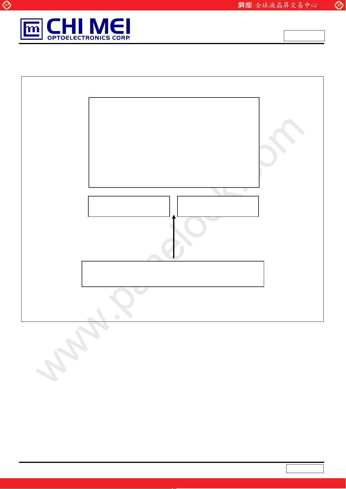
6.2 POWER ON/OFF SEQUENCE
(Ta = 25 ± 2 ºC)
To prevent a latch-up or DC operation of LCD module, the power on/off sequence should be as the diagram
below.
www.panelook.com
Issue Date:Jan. 22.2009
Model No.: V546H1-PH5
Approval
50ms
50ms
ЉЉЉЉ
T4
0V
0
ЉЉЉЉ
T
1
ЉЉЉЉ
10ms
ЉЉЉЉ
T
2
ЉЉЉЉ
ЉЉЉЉ
T
3
ЉЉЉЉ
0
0
1000ms
0.1V
CC
T
3
T1
2
T
0.1V
T4
cc
VALI D
LVDS Signals
0V
Power On
0
ЉЉЉЉ
T
7
ЉЉЉЉ
ЉЉЉЉ
T2
T
8
ЉЉЉЉ
T3
T7
8
T
0
Option Signals
(SELLVDS, EN_DCR
OD_SEL)
Backlight (Recommended)
ЉЉЉЉ
ЉЉЉЉ
T
T5
6
1000ms
100ms
50%
5
T
50%
6
T
Power ON/OFF Sequence
Note (1) The supply voltage of the external system for the module input should follow the definition of Vcc.
Note (2) Apply the lamp voltage within the LCD operation range. When the backlight turns on before the LCD
operation or the LCD turns off before the backlight turns off, the display may momentarily become
abnormal screen.
Note (3) In case of Vcc is in off level, please keep the level of input signals on the low or high impedance. If T2<0,
that maybe cause electrical overstress failure.
Note (4) T4 should be measured after the module has been fully discharged between power off and on period.
Note (5) Interface signal shall not be kept at high impedance when the power is on.
17
One step solution for LCD / PDP / OLED panel application: Datasheet, inventory and accessory!
Version 2.0
www.panelook.com
Page 18

Global LCD Panel Exchange Center
7. OPTICAL CHARACTERISTICS
7.1 TEST CONDITIONS
Item Symbol Value Unit
Ambient Temperature Ta
Ambient Humidity Ha
Supply Voltage VCC 12 V
Input Signal According to typical value in "3. ELECTRICAL CHARACTERISTICS"
Vertical Frame Rate Fr 60 Hz
7.2 OPTICAL SPECIFICATIONS
The relative measurement methods of optical characteristics are shown in 7.2. The following items should be
measured under the test conditions described in 7.1 and stable environment shown in Note (7).
Item Symbol Condition Min. Typ. Max. Unit Note
Contrast Ratio CR
Response Time
Center Transmittance T%
White Variation
Red
Color
Chromaticity
Viewing Angle
Green
Blue
White
Horizontal
Vertical
www.panelook.com
Issue Date:Jan. 22.2009
Model No.: V546H1-PH5
Approval
o
25±2
50±10
3000 4000
Gray to
gray
δW
Rcx
Rcy
Gcx
Gcy
Bcx
Bcy
Wcx 0.333 Wcy
θx+
θ
-
x
θY+
θ
-
Y
θ
=0°, θY =0°
x
With CMO Module
=0°, θY =0°
θ
x
CS-1000T
Standard light source “C”
CR≥20
With CMO Module
-
- 5.6 - %
- - 1.3 -
Typ -
0.03
80 88
80
80
80
4 12
0.655
0.326 -
0.299
0.599 -
0.148
0.099 -
0.372
88 88 88 -
-
Typ +
0.03
-
C
%RH
- (2), (4)
ms (5)
(2), (8)
(2), (7)
-
-
(1),(6)
-
-
Deg. (2), (3)
Note (1) Light source is the standard light source “C” which is defined by CIE and driving voltages are based on
suitable gamma voltages. The calculating method is as following
1. Measure Module’s and BLU’s spectrums. W, R, G, B are with signal input. BLU(for V546H1-LH1) is
supplied by CMO.
2. Calculate cell’s spectrum.
3. Calculate cell’s chromaticity by using the spectrum of standard light source “C”
Note (2) Light source is the BLU which is supplied by CMO and driving voltages are based on suitable gamma
voltages.
Note (3) Definition of Viewing Angle (θx, θy):
Viewing angles are measured by EZ-Contrast 160R (Eldim)
Ǻ
18
One step solution for LCD / PDP / OLED panel application: Datasheet, inventory and accessory!
Version 2.0
www.panelook.com
Page 19

Global LCD Panel Exchange Center
T
www.panelook.com
Issue Date:Jan. 22.2009
Model No.: V546H1-PH5
Approval
Note (4) Definition of Contrast Ratio (CR):
θX- = 90º
6 o’clock
θ
y-
= 90º
The contrast ratio can be calculated by the following expression.
Contrast Ratio (CR) = L255 / L0
x-
y-
Normal
θx = θy = 0º
θy- θy+
θx−
θx+
y+
12 o’clock direction
θ
y+
= 90º
x+
θX+ = 90º
L255: Luminance of gray level 255
L 0: Luminance of gray level 0
CR = CR (1), where CR (X) is corresponding to the Contrast Ratio of the point X at Figure in Note (8).
Note (5) Definition of Gray to Gray Switching Time:
100%
90%
Optical
Response
10%
0%
Gray to Gray
Switching Time
Gray to Gray
ime
Switching Time
Note (6) Measurement Setup:
The LCD module should be stabilized at given temperature for 1 hour to avoid abrupt temperature
change during measuring. In order to stabilize the luminance, the measurement should be executed
after lighting backlight for 1 hour in a windless room.
19
One step solution for LCD / PDP / OLED panel application: Datasheet, inventory and accessory!
Version 2.0
www.panelook.com
Page 20

Global LCD Panel Exchange Center
LCD Module
www.panelook.com
Issue Date:Jan. 22.2009
Model No.: V546H1-PH5
Approval
Note (7) Definition of White Variation (δW):
Measure the luminance of gray level 255 at 5 points
δW = Maximum [L (1), L (2), L (3), L (4), L (5)] / Minimum [L (1), L (2), L (3), L (4), L (5)]
LCD Panel
Center of the Screen
Display Color Analyzer
(Minolta CA210)
Light Shield Room
(Ambient Luminance < 2 lux)
Horizontal Line
D
D/4 D/2 3D/4
W
W/4
W/2
3W /4
Note (8) Definition of Transmittance (T%):
Vertical Line
Module is without signal input.
Transmittance =
1 2
5
3 4
Active Area
Luminance of LCD module
Luminance of backlight
Ϡ
100%
: Test Point
X
X=1 to 5
20
One step solution for LCD / PDP / OLED panel application: Datasheet, inventory and accessory!
Version 2.0
www.panelook.com
Page 21

Global LCD Panel Exchange Center
www.panelook.com
Issue Date:Jan. 22.2009
Model No.: V546H1-PH5
Approval
8. PRECAUTIONS
8.1 ASSEMBLY AND HANDLING PRECAUTIONS
[ 1 ] Do not apply rough force such as bending or twisting to the module during assembly.
[ 2 ] It is recommended to assemble or to install a module into the user’s system in clean working areas. The
dust and oil may cause electrical short or worsen the polarizer.
[ 3 ] Do not apply pressure or impulse to the module to prevent the damage of LCD panel and Backlight.
[ 4 ] Always follow the correct power-on sequence when the LCD module is turned on. This can prevent the
damage and latch-up of the CMOS LSI chips.
[ 5 ] Do not plug in or pull out the I/F connector while the module is in operation.
[ 6 ] Do not disassemble the module.
[ 7 ] Use a soft dry cloth without chemicals for cleaning, because the surface of polarizer is very soft and easily
scratched.
[ 8 ] Moisture can easily penetrate into LCD module and may cause the damage during operation.
[ 9 ] When storing modules as spares for a long time, the following precaution is necessary.
[ 9.1 ] Do not leave the module in high temperature, and high humidity for a long time. It is highly
recommended to store the module with temperature from 0 to 35
condensation.
[ 9.2 ] The module shall be stored in dark place. Do not store the TFT-LCD module in direct sunlight or
fluorescent light.
[ 10 ] When ambient temperature is lower than 10ºC, the display quality might be reduced. For example, the
response time will become slow, and the starting voltage of CCFL will be higher than that of room
temperature.
8.2 SAFETY PRECAUTIONS
[ 1 ] The startup voltage of a Backlight is approximately 1000 Volts. It may cause an electrical shock while
assembling with the inverter. Do not disassemble the module or insert anything into the Backlight unit.
[ 2 ] If the liquid crystal material leaks from the panel, it should be kept away from the eyes or mouth. In case of
contact with hands, skin or clothes, it has to be washed away thoroughly with soap.
[ 3 ] After the module’s end of life, it is not harmful in case of normal operation and storage.
к
at normal humidity without
21
One step solution for LCD / PDP / OLED panel application: Datasheet, inventory and accessory!
Version 2.0
www.panelook.com
Page 22

Global LCD Panel Exchange Center
9. DEFINITION OF LABELS
9.1 OPEN CELL LABEL
The barcode nameplate is pasted on each open cell as illustration for CMO internal control.
9.2 CARTON LABEL
www.panelook.com
Issue Date:Jan. 22.2009
Model No.: V546H1-PH5
Approval
V546H1-PH5
The barcode nameplate is pasted on each box as illustration, and its definitions are as following explanation.
(a) Model Name: V546H1-PH5
(b) Carton ID: CMO internal control
(c) Quantities: 6 pcs
22
One step solution for LCD / PDP / OLED panel application: Datasheet, inventory and accessory!
Version 2.0
www.panelook.com
Page 23

Global LCD Panel Exchange Center
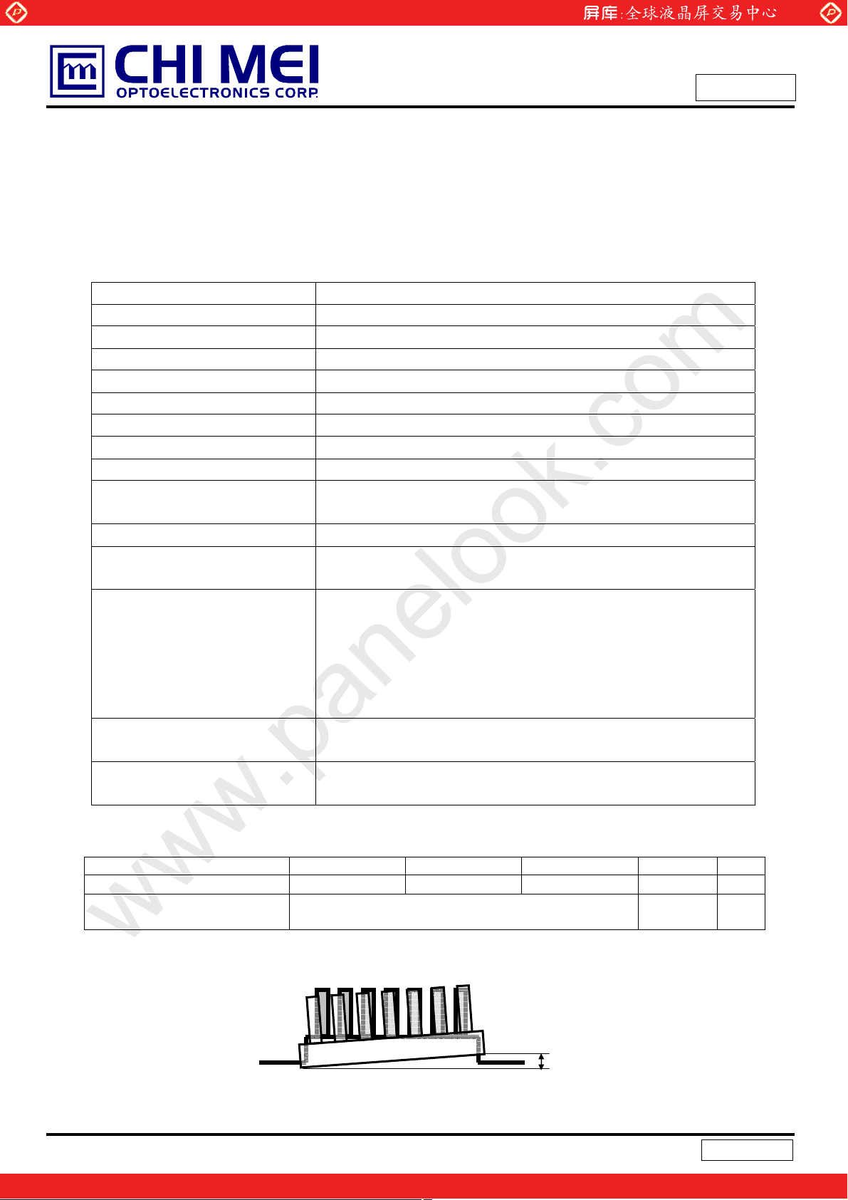
10. PACKAGING
10.1 PACKAGING SPECIFICATIONS
(1) 6 LCD TV Panels / 1 Box
(2) Box dimensions : 1454 (L) X 994 (W) X 210 (H)
(3) Weight : approximately 42Kg ( 6 panels per box)
10.2 PACKAGING METHOD
Figures 10-1 and 10-2 are the packing method
www.panelook.com
Issue Date:Jan. 22.2009
Model No.: V546H1-PH5
Approval
Figure.10-1 packing method
23
One step solution for LCD / PDP / OLED panel application: Datasheet, inventory and accessory!
Version 2.0
www.panelook.com
Page 24

Global LCD Panel Exchange Center
www.panelook.com
Issue Date:Jan. 22.2009
Model No.: V546H1-PH5
Approval
Figure.10-2 packing method
24
One step solution for LCD / PDP / OLED panel application: Datasheet, inventory and accessory!
Version 2.0
www.panelook.com
Page 25

Global LCD Panel Exchange Center
11. MECHANICAL CHARACTERISTICS
www.panelook.com
Issue Date:Jan. 22.2009
Model No.: V546H1-PH5
Approval
ڻႝηިҽԖϦљ
CHI MEI
25
One step solution for LCD / PDP / OLED panel application: Datasheet, inventory and accessory!
Version 2.0
www.panelook.com
Page 26

Global LCD Panel Exchange Center
www.panelook.com
Issue Date:Jan. 22.2009
Model No.: V546H1-PH5
Approval
࡛ભሽٝڶૻֆ
CHI MEI
26
One step solution for LCD / PDP / OLED panel application: Datasheet, inventory and accessory!
Version 2.0
www.panelook.com
Page 27

Global LCD Panel Exchange Center
www.panelook.com
Issue Date:Jan. 22.2009
Model No.: V546H1-PH5
Approval
27
One step solution for LCD / PDP / OLED panel application: Datasheet, inventory and accessory!
Version 2.0
www.panelook.com
Page 28

Global LCD Panel Exchange Center
www.panelook.com
Issue Date:Jan. 22.2009
Model No.: V546H1-PH5
Approval
ڻႝηިҽԖϦљ
CHI MEI
28
One step solution for LCD / PDP / OLED panel application: Datasheet, inventory and accessory!
Version 2.0
www.panelook.com
 Loading...