

Page 1
Global LCD Panel Exchange Center
TFT LCD Approval Specification
MODEL NO.: V470H2 – P01
Customer: _________________________________
www.panelook.com
Issue Date:Sep.21.2009
Model No.: V470H2-P01
Approval
Approved by:_______________________________
Note:
TV Head Division
Approved By
LY Chen
QA Dept. Product Development Div.
Reviewed By
Hsin-nan Chen WT Lin
LCD TV Marketing and Product Management Div.
Prepared By
CY Chang TC Chao
1
One step solution for LCD / PDP / OLED panel application: Datasheet, inventory and accessory!
Version 2.0
www.panelook.com
Page 2
Global LCD Panel Exchange Center
www.panelook.com
Issue Date:Sep.21.2009
Model No.: V470H2-P01
Approval
CONTENTS
REVISION HISTORY ......................................................................................................................................................... 4
1. GENERAL DESCRIPTION ............................................................................................................................................ 5
1.1 OVERVIEW .......................................................................................................................................................... 5
1.2 FEATURES........................................................................................................................................................... 5
1.3 MECHANICAL SPECIFICATIONS ....................................................................................................................... 5
2. ABSOLUTE MAXIMUM RATINGS ................................................................................................................................ 6
2.1 ABSOLUTE RATINGS OF ENVIRONMENT (BASE ON CMO MODULE V470H2-P01) ..................................... 6
2.2 PACKAGE STORAGE .......................................................................................................................................... 7
2.3 ELECTRICAL ABSOLUTE RATINGS .................................................................................................................. 7
2.3.1 ELECTRICAL ABSOLUTE RATINGS (OPEN CELL) ................................................................................ 7
3. ELECTRICAL CHARACTERISTICS ............................................................................................................................. 8
3.1 TFT LCD MODULE .............................................................................................................................................. 8
3.2 Mini-LVDS CHARACTERISTICS ......................................................................................................................... 8
4. BLOCK DIAGRAM OF INTERFACE ............................................................................................................................. 9
4.1 TFT LCD MODULE .............................................................................................................................................. 9
5. INPUT TERMINAL PIN ASSIGNMENT ....................................................................................................................... 10
5.1 TFT LCD Module Input ....................................................................................................................................... 10
5.2 COLOR DATA INPUT ASSIGNMENT ................................................................................................................ 12
6. INTERFACE TIMING ................................................................................................................................................... 13
6.1 INPUT SIGNAL TIMING SPECIFICATIONS(Ta = 25 ± 2 ºC) ............................................................................. 13
6.2 POWER ON/OFF SEQUENCE .......................................................................................................................... 17
7. OPTICAL CHARACTERISTICS .................................................................................................................................. 18
7.1 TEST CONDITIONS ........................................................................................................................................... 18
7.2 OPTICAL SPECIFICATIONS ............................................................................................................................. 18
8. PRECAUTIONS ........................................................................................................................................................... 21
8.1 ASSEMBLY AND HANDLING PRECAUTIONS ................................................................................................. 21
8.2 SAFETY PRECAUTIONS .................................................................................................................................. 21
2
Version 2.0
One step solution for LCD / PDP / OLED panel application: Datasheet, inventory and accessory!
www.panelook.com
Page 3

Global LCD Panel Exchange Center
www.panelook.com
Issue Date:Sep.21.2009
Model No.: V470H2-P01
Approval
9. DEFINITION OF LABELS ............................................................................................................................................ 22
9.1 OPEN CELL LABEL ........................................................................................................................................... 22
9.2 CARTON LABEL ................................................................................................................................................ 22
10. Packaging .................................................................................................................................................................. 23
11. MECHANICAL CHARACTERISTICS ........................................................................................................................ 25
3
One step solution for LCD / PDP / OLED panel application: Datasheet, inventory and accessory!
Version 2.0
www.panelook.com
Page 4
Global LCD Panel Exchange Center
REVISION HISTORY
Version Date Page(New) Section Description
Ver. 1.0 Jun. 11.2009 All All The preliminary specification was first issued.
Ver. 2.0 Sep.21.2009 All All The Approval specification was first issued.
www.panelook.com
Issue Date:Sep.21.2009
Model No.: V470H2-P01
Approval
4
One step solution for LCD / PDP / OLED panel application: Datasheet, inventory and accessory!
Version 2.0
www.panelook.com
Page 5
Global LCD Panel Exchange Center
1. GENERAL DESCRIPTION
1.1 OVERVIEW
V470H2-P01 is a 47” TFT Liquid Crystal Display module with driver ICs and 2ch mini-LVDS interface. This
product supports 1920 x 1080 Full HDTV format and can display 16.7M colors (8-bit/color). The backlight unit is
not built-in.
1.2 FEATURES
CHARACTERISTICS ITEMS SPECIFICATIONS
Screen Diagonal [in] 47”
Pixels [lines] 1920 1080
Active Area [mm] 1039.68 (H) x584.82 (V) (47” diagonal)
Sub-Pixel Pitch [mm] ˃ˁˈˇ˄ˈ(V) ˃ˁ˄ˋ˃ˈ(H)
Pixel Arrangement RGB vertical stripe
Weight [g] 2560
Physical Size [mm] ˄˃ˈˌˁˊˋ(W) ˉ˃ˈˁˋˊ(H) ˄ˁˋ˃(D) Typ.
Display Mode Transmissive mode / Normallly black
Contrast Ratio 4000:1 Typ.
Glass thickness (Array / CF) [mm] 0.7 / 0.7
Viewing Angle (CR>20) +88/-88(H), +88/-88(V) Typ. (CRЊ20)
Color Chromaticity R = (0.649, 0.331)
Cell Transparency [%] 4.5%
Polarizer Surface Treatment Anti-Glare coating (Haze 11%), Hard coating (3H)
www.panelook.com
Issue Date:Sep.21.2009
Model No.: V470H2-P01
Approval
(Typical value measure at CMO’s module)
(Typical value measure at CMO’s module)
G = (0.271, 0.595)
B = (0.148, 0.103)
W= (0.313, 0.349)
* Please refer to “color chromaticity” on p.14
1.3 MECHANICAL SPECIFICATIONS
Item Min. Typ. Max. Unit Note
Weight
I/F connector mounting position
Note (1) Please refer to the attached drawings for more information of front and back outline dimensions.
Note (2) Connector mounting position
The mounting inclination of the connector makes the
screen center within 0.5mm as the horizontal.
˅ˈ˄˃
2560
˅ˉ˄˃
+/- 0.5mm
5
One step solution for LCD / PDP / OLED panel application: Datasheet, inventory and accessory!
g -
(2)
Version 2.0
www.panelook.com
Page 6
Global LCD Panel Exchange Center
www.panelook.com
2. ABSOLUTE MAXIMUM RATINGS
2.1 ABSOLUTE RATINGS OF ENVIRONMENT (BASE ON CMO MODULE V470H2-P01)
Value
Item Symbol
Min. Max.
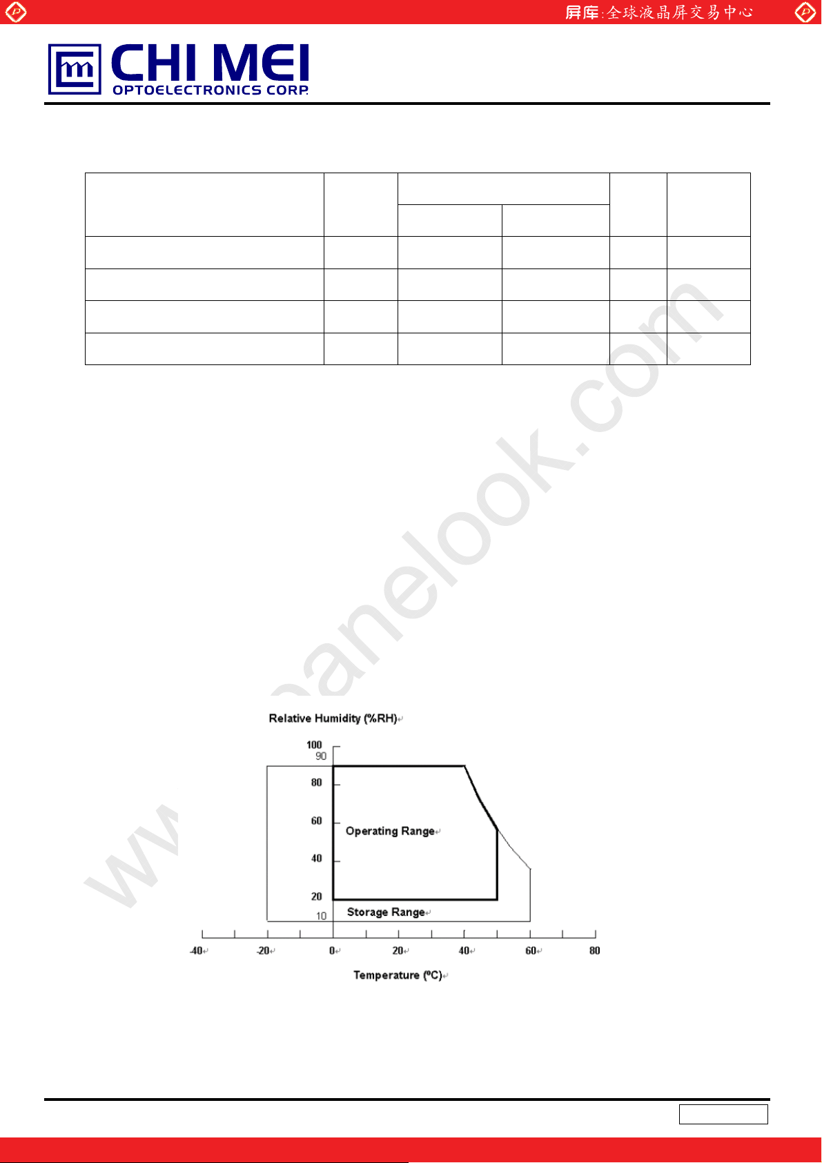
Storage Temperature TST -20 +60 ºC (1)
Operating Ambient Temperature TOP 0 50 ºC (1), (2)
Shock (Non-Operating) SNOP - 50 G (3), (5)
Vibration (Non-Operating) VNOP - 1.0 G (4), (5)
Note (1) Temperature and relative humidity range is shown in the figure below.
(a) 90 %RH Max. (Ta Љ 40 ºC).
Issue Date:Sep.21.2009
Model No.: V470H2-P01
Approval
Unit Note
(b) Wet-bulb temperature should be 39 ºC Max. (Ta > 40 ºC).
(c) No condensation.
Note (2) The maximum operating temperature is based on the test condition that the surface temperature of
display area is less than or equal to 65 ºC with LCD module alone in a temperature controlled chamber.
Thermal management should be considered in final product design to prevent the surface temperature of
display area from being over 65 ºC. The range of operating temperature may degrade in case of
improper thermal management in final product design.
Note (3) 11 ms, half sine wave, 1 time for ± X, ± Y, ± Z.
Note (4) 10 ~ 200 Hz, 10 min, 1 time each X, Y, Z.
Note (5) At testing Vibration and Shock, the fixture in holding the module has to be hard and rigid enough so that
the module would not be twisted or bent by the fixture.
6
One step solution for LCD / PDP / OLED panel application: Datasheet, inventory and accessory!
Version 2.0
www.panelook.com
Page 7
Global LCD Panel Exchange Center
2.2 PACKAGE STORAGE
Storage condition: With shipping package.
Storage temperature rang: 255к
Storage humidity range: 5010%RH
Shelf life: a month
2.3 ELECTRICAL ABSOLUTE RATINGS
2.3.1 ELECTRICAL ABSOLUTE RATINGS (OPEN CELL)
Item Symbol
Power Supply Voltage VAA -0.5 +18.5 V
Power Supply Voltage VGH -0.3 +30.0 V
Power Supply Voltage VGL -10.0 -0.3 V
www.panelook.com
Min. Max.
Issue Date:Sep.21.2009
Model No.: V470H2-P01
Approval
Value
Unit Note
(1)
Logic Input Voltage VDD -0.3 4.0 V
Note (1) Permanent damage to the device may occur if maximum values are exceeded. Function operation
should be restricted to the conditions described under Normal Operating Conditions.
7
One step solution for LCD / PDP / OLED panel application: Datasheet, inventory and accessory!
Version 2.0
www.panelook.com
Page 8
Global LCD Panel Exchange Center
3. ELECTRICAL CHARACTERISTICS
3.1 TFT LCD MODULE
(Ta = 25 ± 2 ºC)
Parameter Symbol
www.panelook.com
Issue Date:Sep.21.2009
Model No.: V470H2-P01
Approval
Value
Unit Note
Min. Typ. Max.
29 30 31 V
V
GH
VGL -8.5 -8.0 -7.5 V
Power Supply Voltage
VAA 17.4 17.7 18 V
VDD 3.2 3.3 3.4 V
V
16.85 17.00 17.15 V
REF
I
- 15 mA
GH
IGL - 8 - mA
Power Supply Current
IAA - 380 - mA
IDD 250 mA
CMOS
interface
Input High Threshold Voltage V
Input Low Threshold Voltage VIL 0 - 0.3VDD V
0.7VDD - VDD V
IH
Note (1) The module should be always operated within the above ranges.
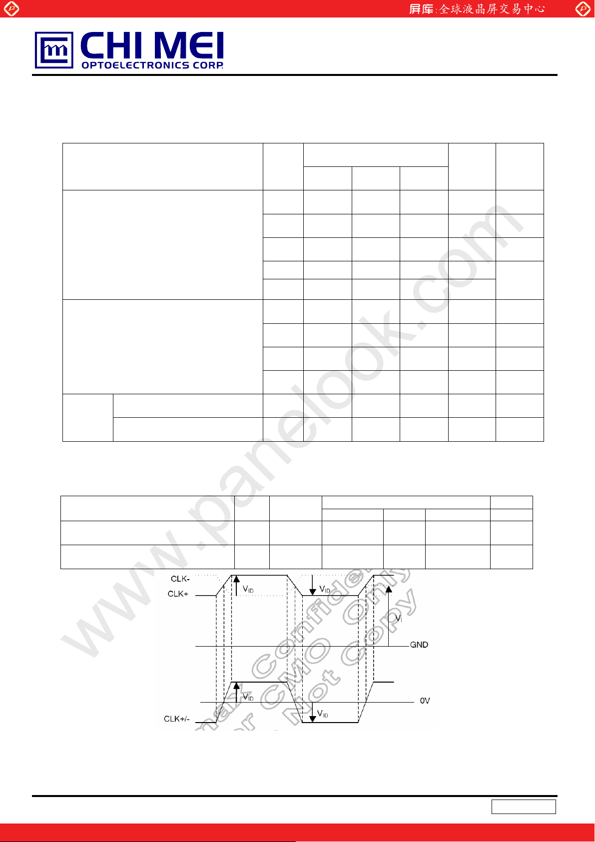
3.2 Mini-LVDS CHARACTERISTICS
(Ta = -20 to + 85 ºC)
Item Symbol Condition
mini-LVDS differential voltage
(amplitude: peak to peak)
mini-LVDS common mode input
voltage range (center)
V
ID
V
I
-
VSS+0.5 1.2 VDD-1.2 V
Value Unit
Min. Typ. Max.
100 - 600 mV
8
One step solution for LCD / PDP / OLED panel application: Datasheet, inventory and accessory!
Version 2.0
www.panelook.com
Page 9

Global LCD Panel Exchange Center
4. BLOCK DIAGRAM OF INTERFACE
4.1 TFT LCD MODULE
www.panelook.com
Issue Date:Sep.21.2009
Model No.: V470H2-P01
Approval
TFT LCD PANEL
(1920x3x1080)
X(R) Board X(L) Board
Mini-LVDS Signal Input
9
One step solution for LCD / PDP / OLED panel application: Datasheet, inventory and accessory!
Version 2.0
www.panelook.com
Page 10

Global LCD Panel Exchange Center
www.panelook.com
5. INPUT TERMINAL PIN ASSIGNMENT
5.1 TFT LCD Module Input
Pin assignment
CN1(XL) Connector Pin Assignment
Pin Symbol Description Pin Symbol Description
1 GND Ground 41 GM6 Gamma Power supply
2 NC
3 NC
4 GND Ground 44 GM3 Gamma Power supply
5 NC
6 NC
7 NC
8 NC
9 NC
10 NC
11 GND Ground 51 GND Ground
12 ML5N_F Mini-LVDS data input 52 VAA
13 ML5P_F Mini-LVDS data input 53 VAA
14 ML4N_F Mini-LVDS data input 54 GND Ground
15 ML4P_F Mini-LVDS data input 55 VDD
16 ML3N_F Mini-LVDS data input 56 VDD
17 ML3P_F Mini-LVDS data input 57 GND Ground
18 GND Ground 58
19 CLKN_F Mini-LVDS Clock input 59
20 CLKP_F Mini-LVDS Clock input 60 GND Ground
21 GND Ground 61 NC
22 ML2N_F Mini-LVDS data input 62 VCM VCM Power supply
23 ML2P_F Mini-LVDS data input 63 VCM VCM Power supply
24 ML1N_F Mini-LVDS data input 64 GND Ground
25 ML1P_F Mini-LVDS data input 65 VGL
26 ML0N_F Mini-LVDS data input 66 OE1
27 ML0P_F Mini-LVDS data input 67 CKV
28 GND Ground 68 STV
29 GM18 Gamma Power supply 69 GND Ground
30 GM17 Gamma Power supply 70 OE2
31 GM16 Gamma Power supply 71 NC
32 GM15 Gamma Power supply 72 NC
33 GM14 Gamma Power supply 73 NC
34 GM13 Gamma Power supply 74 NC
35 GM12 Gamma Power supply 75 NC
36 GM11 Gamma Power supply 76 NC
37 GM10 Gamma Power supply 77 NC
38 GM9 Gamma Power supply 78 NC
39 GM8 Gamma Power supply 79 NC
40 GM7 Gamma Power supply 80 GND Ground
No connection
No connection
No connection
No connection
No connection
No connection
No connection
No connection
42 GM5 Gamma Power supply
43 GM4 Gamma Power supply
45 GM2 Gamma Power supply
46 GM1 Gamma Power supply
47 GND Ground
48 NC
49 POL
50 A_TP1
VGH Driver Power supply
VGH Driver Power supply
No connection
Polarity invert
Mini-LVDS data latch input
Driver power supply
Driver power supply
Logic Power supply
Logic Power supply
No connection
Driver Power supply
Scan driver output enable
Scan driver clock
Scan driver start pulse
Scan driver output enable
No connection
No connection
No connection
No connection
No connection
No connection
No connection
No connection
No connection
Issue Date:Sep.21.2009
Model No.: V470H2-P01
Approval
10
One step solution for LCD / PDP / OLED panel application: Datasheet, inventory and accessory!
Version 2.0
www.panelook.com
Page 11

Global LCD Panel Exchange Center
CN1(XR) Connector Pin Assignment
Pin No. Symbol Description Pin No. Symbol Description
1 GND Ground 41 GM12 Gamma Power supply
2 VSCM
3 NC
4 NC
5 NC
6 NC
7 NC
8 NC
9 NC
10 NC
11 O E2
12 GND Ground 52 GM1 Gamma Power supply
13 OE1
14 CKV
15 STV
16 VGL
17 GND Ground 57 ML4P_B Mini-LVDS data input
18 VCM VCM Power supply 58 ML3N_B Mini-LVDS data input
19 VCM VCM Power supply 59 ML3P_B Mini-LVDS data input
20 NC
VCM adjust from VR
No connection
No connection
No connection
No connection
No connection
No connection
No connection
No connection
Scan driver output enable
Scan driver output enable
Scan driver clock
Scan driver start pulse
Driver Power supply
No connection
www.panelook.com
Issue Date:Sep.21.2009
Model No.: V470H2-P01
42 GM11 Gamma Power supply
43 GM10 Gamma Power supply
44 GM9 Gamma Power supply
45 GM8 Gamma Power supply
46 GM7 Gamma Power supply
47 GM6 Gamma Power supply
48 GM5 Gamma Power supply
49 GM4 Gamma Power supply
50 GM3 Gamma Power supply
51 GM2 Gamma Power supply
53 GND Ground
54 ML5N_B Mini-LVDS data input
55 ML5P_B Mini-LVDS data input
56 ML4N_B Mini-LVDS data input
60 GND Ground
Approval
21 GND Ground 61 CLKN_B Mini-LVDS Clock input
22
23
24 GND Ground 64 ML2N_B Mini-LVDS data input
25 VDD
26 VDD
27 GND Ground 67 ML1P_B Mini-LVDS data input
28 VAA
29 VAA
30 GND Ground 70 GND Ground
31 POL
32 B_TP1
33 NC
34 GND Ground 74 NC
35 GM18 Gamma Power supply 75 NC
36 GM17 Gamma Power supply 76 NC
37 GM16 Gamma Power supply 77 GND Ground
38 GM15 Gamma Power supply 78 NC
39 GM14 Gamma Power supply 79 NC
40 GM13 Gamma Power supply 80 GND Ground
Note (1) CN1Ε2 Connector Part No.: GB5RF801-125C-7F,Foxconn KunShan(༄Փൈ࣒՞) or equal.
Note (2) The OE1 and OE2 must be connected to the OE.
VGH Driver Power supply
VGH Driver Power supply
Logic Power supply
Logic Power supply
Driver power supply
Driver power supply
Polarity invert
Mini-LVDS data latch input
No connection
62 CLKP_B Mini-LVDS Clock input
63 GND Ground
65 ML2P_B Mini-LVDS data input
66 ML1N_B Mini-LVDS data input
68 ML0N_B Mini-LVDS data input
69 ML0P_B Mini-LVDS data input
71 NC
72 NC
73 NC
No connection
No connection
No connection
No connection
No connection
No connection
No connection
No connection
11
One step solution for LCD / PDP / OLED panel application: Datasheet, inventory and accessory!
Version 2.0
www.panelook.com
Page 12

Global LCD Panel Exchange Center
5.2 COLOR DATA INPUT ASSIGNMENT
The brightness of each primary color (red, green and blue) is based on the 8-bit gray scale data input for the color.
The higher the binary input, the brighter the color. The table below provides the assignment of the color versus
data input.
Color
R7 R6 R5 R4 R3 R2 R1 R0 G7 G6 G5 G4 G3 G2 G1 G0 B7 B6 B5 B4 B3 B2 B1 B0
Black
Red
Green
Basic
Colors
Gray
Scale
Of
Red
Gray
Scale
Of
Green
Gray
Scale
Of
Blue
Note (1) 0: Low Level Voltage, 1: High Level Voltage
Blue
Cyan
Magenta
Yellow
White
Red (0) / Dark
Red (1)
Red (2)
:
:
Red (253)
Red (254)
Red (255)
Green (0) / Dark
Green (1)
Green (2)
:
:
Green (253)
Green (254)
Green (255)
Blue (0) / Dark
Blue (1)
Blue (2)
:
:
Blue (253)
Blue (254)
Blue (255)
0
0
0
1
1
1
0
0
0
0
0
0
0
0
0
1
1
1
1
1
1
1
1
1
0
0
0
0
0
0
0
0
0
:
:
:
:
:
:
1
1
1
1
1
1
1
1
1
0
0
0
0
0
0
0
0
0
:
:
:
:
:
:
0
0
0
0
0
0
0
0
0
0
0
0
0
0
0
0
0
0
:
:
:
:
:
:
0
0
0
0
0
0
0
0
0
www.panelook.com
Issue Date:Sep.21.2009
Model No.: V470H2-P01
Approval
Data Signal
Red Green Blue
0
0
0
0
0
0
0
0
0
0
0
0
0
0
0
0
0
0
0
0
0
1
1
1
1
1
0
0
0
0
0
0
0
0
0
0
0
0
0
0
0
0
0
0
0
0
0
1
1
1
1
1
1
1
1
0
0
0
0
0
0
0
0
0
0
0
0
0
0
0
0
0
0
0
0
0
1
1
1
1
1
1
1
1
0
0
0
0
0
1
1
1
1
1
1
1
1
1
1
1
1
1
1
1
1
1
1
1
1
1
0
0
0
0
0
0
0
0
1
1
1
1
1
1
1
1
1
1
1
1
1
1
1
1
1
1
1
1
1
0
0
0
0
0
0
0
0
1
1
1
1
1
1
1
1
1
1
1
1
1
1
1
1
1
1
1
1
1
0
0
0
0
0
0
0
0
0
0
0
0
0
0
0
0
0
0
0
0
0
0
0
0
0
1
0
0
0
0
0
0
0
0
0
0
0
0
0
0
0
0
0
0
0
1
0
0
0
0
0
0
0
0
0
0
0
0
0
0
0
0
0
:
:
:
:
:
:
:
:
:
:
:
:
:
:
:
:
:
:
:
:
:
:
:
:
:
:
:
:
:
:
:
:
:
:
:
:
:
:
:
:
:
:
1
1
1
0
1
0
0
0
0
0
0
0
0
0
0
0
0
0
0
0
0
1
1
1
1
0
0
0
0
0
0
0
0
0
0
0
0
0
0
0
0
0
1
1
1
1
1
0
0
0
0
0
0
0
0
0
0
0
0
0
0
0
0
0
0
0
0
0
0
0
0
0
0
0
0
0
0
0
0
0
0
0
0
0
0
0
0
0
0
0
0
0
0
0
0
0
1
0
0
0
0
0
0
0
0
0
0
0
0
0
0
0
0
0
0
0
1
0
0
0
0
0
0
0
0
0
:
:
:
:
:
:
:
:
:
:
:
:
:
:
:
:
:
:
:
:
:
:
:
:
:
:
:
:
:
:
:
:
:
:
:
:
:
:
:
:
:
:
0
0
0
0
0
1
1
1
1
1
1
0
1
0
0
0
0
0
0
0
0
0
0
0
0
0
1
1
1
1
1
1
1
0
0
0
0
0
0
0
0
0
0
0
0
0
0
1
1
1
1
1
1
1
1
0
0
0
0
0
0
0
0
0
0
0
0
0
0
0
0
0
0
0
0
0
0
0
0
0
0
0
0
0
0
0
0
0
0
0
0
0
0
0
0
0
0
0
0
0
0
0
0
0
1
0
0
0
0
0
0
0
0
0
0
0
0
0
0
0
0
0
0
0
1
0
:
:
:
:
:
:
:
:
:
:
:
:
:
:
:
:
:
:
:
:
:
:
:
:
:
:
:
:
:
:
:
:
:
:
:
:
:
:
:
:
:
:
0
0
0
0
0
0
0
0
0
0
0
0
0
1
1
1
1
1
1
0
1
0
0
0
0
0
0
0
0
0
0
0
0
0
1
1
1
1
1
1
1
0
0
0
0
0
0
0
0
0
0
0
0
0
0
1
1
1
1
1
1
1
1
12
One step solution for LCD / PDP / OLED panel application: Datasheet, inventory and accessory!
Version 2.0
www.panelook.com
Page 13

Global LCD Panel Exchange Center
www.panelook.com
6. INTERFACE TIMING
6.1 INPUT SIGNAL TIMING SPECIFICATIONS(Ta = 25 ± 2 ºC)
(a) Timing Spec
Parameter Symbol Condition
Clock period tCLK - 4
Clock low pulse width tCLK(L) - 1.7 - - ns
Clock high pulse width tCLK(H) - 1.7 - - ns
Data setup time tSETUP1 - 0.8 - - ns
Data hold time tHOLD1 - 0.8 - - ns
CLK,LV [5:0] rising time tRISE - - 0.8 ns
CLK,LV [5:0] falling time tFALL - - 0.8 ns
Start pulse setup time tSETUP2 0 - - ns
PLH1 Loading=15pF - - 13 ns
t
Start pulse delay time
tPHL1 Loading=15pF - - 13 ns
HD
Reset(RST) high time tRESETH
TP1 high period tTP1(H) 200 - - ns
POL to TP1 setup time tPOL-TP1 POL toggle to TP1 rising 5 - - ns
Issue Date:Sep.21.2009
Model No.: V470H2-P01
Approval
Spec
Min. Typ. Max.
(1)
50ns
over 3
CLK
-
- - -
-
Unit
ns
TP1 to POL hold time tTP1-POL TP1 falling to POL toggle 6 - - ns
Receiver off to TP1 timing tREC-OFF 5 - - CLK
TP1 to reset input time tTP-RESET 200 - - ns
Reset low to TP1 rising time tRESET-TP1 0 ns
Output delay time1 tPD1 CL=100pF - - 5
Output delay time2 tPD2 CL=100pF - - 10
Output delay time3 tPD3 CL=100Pf - - 5
Output delay time4 tPD4 CL=100pF - - 10
CKV period t
CKV pulse width tCKVH, tCKVL 50% duty cycle 2.5 - -
OE pulse width tWOE - 1 - -
Data setup time
VD
Data hold time
tSU
tHD
CKV to output delay time tPD1 CL=300pF - - 1
Start pulse output delay time tPD2 - CL=300pF - - 0.8
OE to output delay time tPD3 CL=300pF - - 0.8
Note (1) : When operation frequency=250MHz
Ӵs
Ӵs
Ӵs
Ӵs
CKV - 5 - -
Ӵs
Ӵs
Ӵs
0.5 - -
0.5 - -
Ӵs
Ӵs
Ӵs
Ӵs
Ӵs
13
One step solution for LCD / PDP / OLED panel application: Datasheet, inventory and accessory!
Version 2.0
www.panelook.com
Page 14

Global LCD Panel Exchange Center
(b) Horizontal Timing Chart
www.panelook.com
Issue Date:Sep.21.2009
Model No.: V470H2-P01
Approval
14
One step solution for LCD / PDP / OLED panel application: Datasheet, inventory and accessory!
Version 2.0
www.panelook.com
Page 15

Global LCD Panel Exchange Center
Last data sampling to TP1 timing for 726 channel case:
www.panelook.com
Issue Date:Sep.21.2009
Model No.: V470H2-P01
Approval
Relationship between EIO(OUT)and EIO(IN) timing for 726 channel case:
15
One step solution for LCD / PDP / OLED panel application: Datasheet, inventory and accessory!
Version 2.0
www.panelook.com
Page 16

Global LCD Panel Exchange Center
(c)Vertical Timing Chart
www.panelook.com
Issue Date:Sep.21.2009
Model No.: V470H2-P01
Approval
16
One step solution for LCD / PDP / OLED panel application: Datasheet, inventory and accessory!
Version 2.0
www.panelook.com
Page 17

Global LCD Panel Exchange Center
6.2 POWER ON/OFF SEQUENCE
To prevent the device from damage due to latch up , the power ON/OFF sequence shown below must be
followed.
When power on : VDD Ш VGL Ш VAA Ш VGH , Input signal (t1Ї0)
When power off : Input signal , VGH Ш VAA Ш VGL Ш VDD (t2Њ0)
www.panelook.com
Issue Date:Sep.21.2009
Model No.: V470H2-P01
Approval
VGH
VAA
VSSD,VSSA
VDD
Input signal
t
t1 t2
VGL
17
One step solution for LCD / PDP / OLED panel application: Datasheet, inventory and accessory!
Version 2.0
www.panelook.com
Page 18

Global LCD Panel Exchange Center
x
Y
7. OPTICAL CHARACTERISTICS
7.1 TEST CONDITIONS
Item Symbol Value Unit
Ambient Temperature Ta
Ambient Humidity Ha
Supply Voltage VCC 12 V
Input Signal According to typical value in "3. ELECTRICAL CHARACTERISTICS"
Lamp Current I
Oscillating Frequency (Inverter) F
Vertical Frame Rate Fr 60 Hz
7.2 OPTICAL SPECIFICATIONS
The relative measurement methods of optical characteristics are shown in 7.2. The following items should be
measured under the test conditions described in 7.1 and stable environment shown in Note (7).
Item Symbol Condition Min. Typ. Max. Unit Note
Red
Green
Color
Chromaticity
Blue
White
Center Transmittance T%
Contrast Ratio CR
Response Time
White Variation
Horizontal
Viewing Angle
Vertica l
www.panelook.com
Issue Date:Sep.21.2009
Model No.: V470H2-P01
Approval
o
r2
25
50r10
L
W
Rcx
Rcy
9.3r0.5
40r3
(0.649)
(0.331) -
Gcx (0.271) -
=0q, TY =0q
T
Gcy
Bcx (0.148) Bcy
Standard light source “C”
x
CS-1000T
Typ -
(0.595) -
0.03
Typ +
0.03
(0.103) Wcx (0.313) Wcy
Gray to
gray
GW
T
+
Tx-
T
+
TY-
=0q, TY =0q
T
x
With CMO Module
=0q, TY =0q
T
x
With CMO Module
@60Hz
T
=0q, TY =0q
x
With CMO Module
CRt20
With CMO Module
(3000) (4000)
(0.349) -
- (4.5) - -
(6.5) (12)
-
- - (1.3)
(80) (88)
(80)
(80)
(80)
(88)
(88)
(88)
-
-
-
-
C
%RH
mA
KHz
-
(1),(6)
(2), (8)
(2), (4)
-
(5)
(2), (7)
Deg. (2), (3)
Note (1) Light source is the standard light source ”C” which is defined by CIE and driving voltage are based on
suitable gamma voltages. The calculating method is as following :
1. Measure Module’s and BLU’s spectrum. White is without signal input and R,G,B are with signal input.
BLU(for V470H2-L01) is supplied by CMO.
2. Calculate cell’s spectrum.
3. Calculate cell’s chromaticity by using the spectrum of standard light source “C”.
Note (2) Light source is the BLU which is supplied by CMO and driving voltages are based on suitable gamma
voltages.
Note (3) Definition of Viewing Angle (Tx, Ty):
Viewing angles are measured by Conoscope Cono-80
18
One step solution for LCD / PDP / OLED panel application: Datasheet, inventory and accessory!
Version 2.0
www.panelook.com
Page 19

Global LCD Panel Exchange Center
www.panelook.com
Issue Date:Sep.21.2009
Model No.: V470H2-P01
Approval
Normal
Tx = Ty = 0º
Ty- Ty
TX- = 90º
6 o’clock
T
y- = 90º
Note (4) Definition of Contrast Ratio (CR):
The contrast ratio can be calculated by the following expression.
Contrast Ratio (CR) = L255 / L0
L255: Luminance of gray level 255
L 0: Luminance of gray level 0
CR = CR (1), where CR (X) is corresponding to the Contrast Ratio of the point X at Figure in Note (8).
Note (5) Definition of Gray to Gray Switching Time:
x-
Tx
y-
Tx
y+
12 o’clock direction
T
y+ = 90º
x+
TX+ = 90º
100%
90%
Optical
Response
10%
0%
Note (6) Measurement Setup:
The LCD module should be stabilized at given temperature for 1 hour to avoid abrupt temperature
change during measuring. In order to stabilize the luminance, the measurement should be executed
Gray to Gray
Switching Time
Gray to Gray
Time
Switching Time
19
Version 2.0
One step solution for LCD / PDP / OLED panel application: Datasheet, inventory and accessory!
www.panelook.com
Page 20

Global LCD Panel Exchange Center
after lighting backlight for 1 hour in a windless room.
LCD M odule
LCD P anel
Field of View = 1º
www.panelook.com
Issue Date:Sep.21.2009
Model No.: V470H2-P01
Approval
CS -2000
500 mm
Note (7) Definition of White Variation (GW):
Measure the luminance of gray level 255 at 5 points
GW = Maximum [L (1), L (2), L (3), L (4), L (5)] / Minimum [L (1), L (2), L (3), L (4), L (5)]
W/4
W/2
W
Vertical Line
3W/4
Light Shield Room
(Ambient Luminance < 2 lux)
Horizontal Line
D
D/4 D/2 3D/4
1 2
5
3 4
X
: Test Point
X=1 to 5
Active Area
Note (8) Definition of Transmittance (T%):
Module is without signal input.
Luminance of LCD module
Transmittance =
Ϡ 100%
Luminance of backlight
20
One step solution for LCD / PDP / OLED panel application: Datasheet, inventory and accessory!
Version 2.0
www.panelook.com
Page 21

Global LCD Panel Exchange Center
www.panelook.com
Issue Date:Sep.21.2009
Model No.: V470H2-P01
Approval
8. PRECAUTIONS
8.1 ASSEMBLY AND HANDLING PRECAUTIONS
[ 1 ] Do not apply rough force such as bending or twisting to the module during assembly.
[ 2 ] It is recommended to assemble or to install a module into the user’s system in clean working areas. The
dust and oil may cause electrical short or worsen the polarizer.
[ 3 ] Do not apply pressure or impulse to the module to prevent the damage of LCD panel and Backlight.
[ 4 ] Always follow the correct power-on sequence when the LCD module is turned on. This can prevent the
damage and latch-up of the CMOS LSI chips.
[ 5 ] Do not plug in or pull out the I/F connector while the module is in operation.
[ 6 ] Do not disassemble the module.
[ 7 ] Use a soft dry cloth without chemicals for cleaning, because the surface of polarizer is very soft and easily
scratched.
[ 8 ] Moisture can easily penetrate into LCD module and may cause the damage during operation.
[ 9 ] When storing modules as spares for a long time, the following precaution is necessary.
[ 9.1 ] Do not leave the module in high temperature, and high humidity for a long time. It is highly
recommended to store the module with temperature from 0 to 35кat normal humidity without
condensation.
[ 9.2 ] The module shall be stored in dark place. Do not store the TFT-LCD module in direct sunlight or
fluorescent light.
[ 10 ] When ambient temperature is lower than 10ºC, the display quality might be reduced. For example, the
response time will become slow, and the starting voltage of CCFL will be higher than that of room
temperature.
8.2 SAFETY PRECAUTIONS
[ 1 ] The startup voltage of a Backlight is approximately 1000 Volts. It may cause an electrical shock while
assembling with the inverter. Do not disassemble the module or insert anything into the Backlight unit.
[ 2 ] If the liquid crystal material leaks from the panel, it should be kept away from the eyes or mouth. In case of
contact with hands, skin or clothes, it has to be washed away thoroughly with soap.
[ 3 ] After the module’s end of life, it is not harmful in case of normal operation and storage.
21
One step solution for LCD / PDP / OLED panel application: Datasheet, inventory and accessory!
Version 2.0
www.panelook.com
Page 22

Global LCD Panel Exchange Center
9. DEFINITION OF LABELS
9.1 OPEN CELL LABEL
The barcode nameplate is pasted on each open cell as illustration for CMO internal control.
9.2 CARTON LABEL
www.panelook.com
Issue Date:Sep.21.2009
Model No.: V470H2-P01
Approval
V470H2-P01
The barcode nameplate is pasted on each box as illustration, and its definitions are as following explanation.
(a) Model Name: V470H2-P01
(b) Carton ID: CMO internal control
(c) Quantities: 8 pcs
22
One step solution for LCD / PDP / OLED panel application: Datasheet, inventory and accessory!
Version 2.0
www.panelook.com
Page 23

Global LCD Panel Exchange Center
10. Packaging
10.1 packing specifications
(1) 8 LCD TV Panels / 1 Box
(2) Box dimensions :1238 (L) X 842 (W) X 240(H)
(3) Weight : approximately 38Kg (8 panels per box)
10.2 packing Method
Figures 10-1 and 10-2 are the packing method
www.panelook.com
Issue Date:Sep.21.2009
Model No.: V470H2-P01
Approval
Panel
Panel
Carton
Top layer for empty tray
Figure.10-1 packing method
Tape
Carton Label
23
One step solution for LCD / PDP / OLED panel application: Datasheet, inventory and accessory!
Version 2.0
www.panelook.com
Page 24

Global LCD Panel Exchange Center
www.panelook.com
Issue Date:Sep.21.2009
Model No.: V470H2-P01
Approval
Figure.10-2 packing method
24
One step solution for LCD / PDP / OLED panel application: Datasheet, inventory and accessory!
Version 2.0
www.panelook.com
Page 25

Global LCD Panel Exchange Center
11. MECHANICAL CHARACTERISTICS
www.panelook.com
Issue Date:Sep.21.2009
Model No.: V470H2-P01
Approval
࡛ભሽٝڶૻֆ
%*+/'+
25
One step solution for LCD / PDP / OLED panel application: Datasheet, inventory and accessory!
Version 2.0
www.panelook.com
 Loading...