

Page 1
Global LCD Panel Exchange Center
TFT LCD Preliminary Specification
MODEL NO.:V460H1-P06
www.panelook.com
Issued Date: Jun. 17, 2009
Model No.: V460H1-P06
Preliminary
TVHD
Approved By
LY Chen
QRA Dept. Product Development Div.
Reviewed By
Hsin-nan Chen WT Lin
LCD TV Marketing and Product Management Div.
Prepared By
Josh Chi Jim Ho
1
One step solution for LCD / PDP / OLED panel application: Datasheet, inventory and accessory!
Version 1.0
www.panelook.com
Page 2
Global LCD Panel Exchange Center
www.panelook.com
Issued Date: Jun. 17, 2009
Model No.: V460H1-P06
Preliminary
- CONTENTS -
REVISION HISTORY
1. GENERAL DESCRIPTION
1.1 OVERVIEW
1.2 CHARACTERISTICS
1.3 MECHANICAL SPECIFICATIONS
2. ABSOLUTE MAXIMUM RATINGS
2.1 ABSOLUTE RATINGS OF ENVIRONMENT (BASED ON CMO MODULE V460H1-L06)
2.2 ABSOLUTE RATINGS OF ENVIRONMENT (OPEN CELL)
2.3 ELECTRICAL ABSOLUTE RATINGS (OPEN CELL)
3. ELECTRICAL CHARACTERISTICS
3.1 TFT LCD OPEN CELL
3.2 MINI-LVDS CHARACTERISTICS
4. BLOCK DIAGRAM
4.1 TFT LCD OPEN CELL
5. INTERFACE TIMING
6. INPUT TERMINAL PIN ASSIGNMENT
6.1 INPUT SIGNAL TIMING SPECIFICATIONS
6.2.POWER ON/OFF SEQUENCE
-------------------------------------------------------
-------------------------------------------------------
-------------------------------------------------------
-------------------------------------------------------
-------------------------------------------------------
------------------------------------------------------- 9
------------------------------------------------------- 11
3
4
5
7
8
7. OPTICAL CHARACTERISTICS
7.1 TEST CONDITIONS
7.2 OPTICAL SPECIFICATIONS
8. DEFINITION OF LABELS
8.1 OPEN CELL LABEL
8.2 CARTON LABEL
9. PACKAGING
9.1 PACKING SPECIFICATIONS
9.2 PACKING METHOD
10. PRECAUTIONS
10.1 ASSEMBLY AND HANDLING PRECAUTIONS
10.2 SAFETY PRECAUTIONS
11. MECHANICAL DRAWING
-------------------------------------------------------
-------------------------------------------------------
-------------------------------------------------------
-------------------------------------------------------
-------------------------------------------------------
16
20
21
23
24
2
One step solution for LCD / PDP / OLED panel application: Datasheet, inventory and accessory!
Version 1.0
www.panelook.com
Page 3
Global LCD Panel Exchange Center
www.panelook.com
Issued Date: Jun. 17, 2009
Model No.: V460H1-P06
Preliminary
REVISION HISTORY
Version Date
Page
(New)
Ver 1.0 Jun.17, 2009 All All Preliminary Specification was first issued.
Section Description
3
One step solution for LCD / PDP / OLED panel application: Datasheet, inventory and accessory!
Version 1.0
www.panelook.com
Page 4
Global LCD Panel Exchange Center
1. GENERAL DESCRIPTION
1.1 OVERVIEW
V460H1- P06 is a 46” TFT Liquid Crystal Display module. This module supports 1920 x 1080 HDTV format
and can display true 16.7M colors (8bit/color).
1.2 CHARACTERISTICS
CHARACTERISTICS ITEMS SPECIFICATIONS
Screen Diagonal [in] 46
Pixels [lines] 1920 x 1080
Active Area [mm] 1018.08(H) x 572.67(V) (46” diagonal)
Sub -Pixel Pitch [mm] 0.17675(H) x 0.53025(V)
Pixel Arrangement RGB vertical stripe
Weight [g] TYP. 2490 ʳ
www.panelook.com
Issued Date: Jun. 17, 2009
Model No.: V460H1-P06
Preliminary
Physical Size [mm] 1056.38(W) x 628.52(H) x 2(D) Typ.
Display Mode Transmissive mode / Normally black
Contrast Ratio
Glass thickness (Array/CF) [mm] 0.7 / 0.7
Viewing Angle (CR>20)
Color Chromaticity
Cell Transparency [и]
Polarizer (CF side)
5000:1 Typ.
(Typical value measured at CMO’s module)
+88/-88(H),+88/-88(V) Typ.
(Typical value measured at CMO’s module)
R=(0.643, 0.323)
G=(0.287, 0.602)
B=(0.148, 0.056)
W=(0.280, 0.290)
(Typical value measured at CMO’s module)
4.4%Typ.
(Typical value measured at CMO’s module)
Super Wide View, Anti-Glare coating, 1030.18 (H) x
586.37(w).. Hardness: 3H
Polarizer (TFT side) Super Wide View, 1030.18(H) x 586.37(w).
1.3 MECHANICAL SPECIFICATIONS
Item Min. Typ. Max. Unit Note
Weight - 2490 - g -
I/F connector mounting position
Note (1) Please refer to the attached drawings for more information of front and back outline dimensions.
(2) Connector mounting position
The mounting inclination of the connector makes
the screen center within ±0.5mm as the horizontal.
+/- 0.5mm
4
(2)
One step solution for LCD / PDP / OLED panel application: Datasheet, inventory and accessory!
Version 1.0
www.panelook.com
Page 5
Global LCD Panel Exchange Center
www.panelook.com
Issued Date: Jun. 17, 2009
Model No.: V460H1-P06
2. ABSOLUTE MAXIMUM RATINGS
2.1 ABSOLUTE RATINGS OF ENVIRONMENT (BASED ON CMO MODULE V460H1-PH1)
Item Symbol
Storage Temperature TST -20 +60 ºC (1), (3)
Operating Ambient Temperature TOP 0 50 ºC (1), (2), (3)
Altitude Operating A OP 0 5000 M (3)
Altitude Storage A ST 0 12000 M (3)
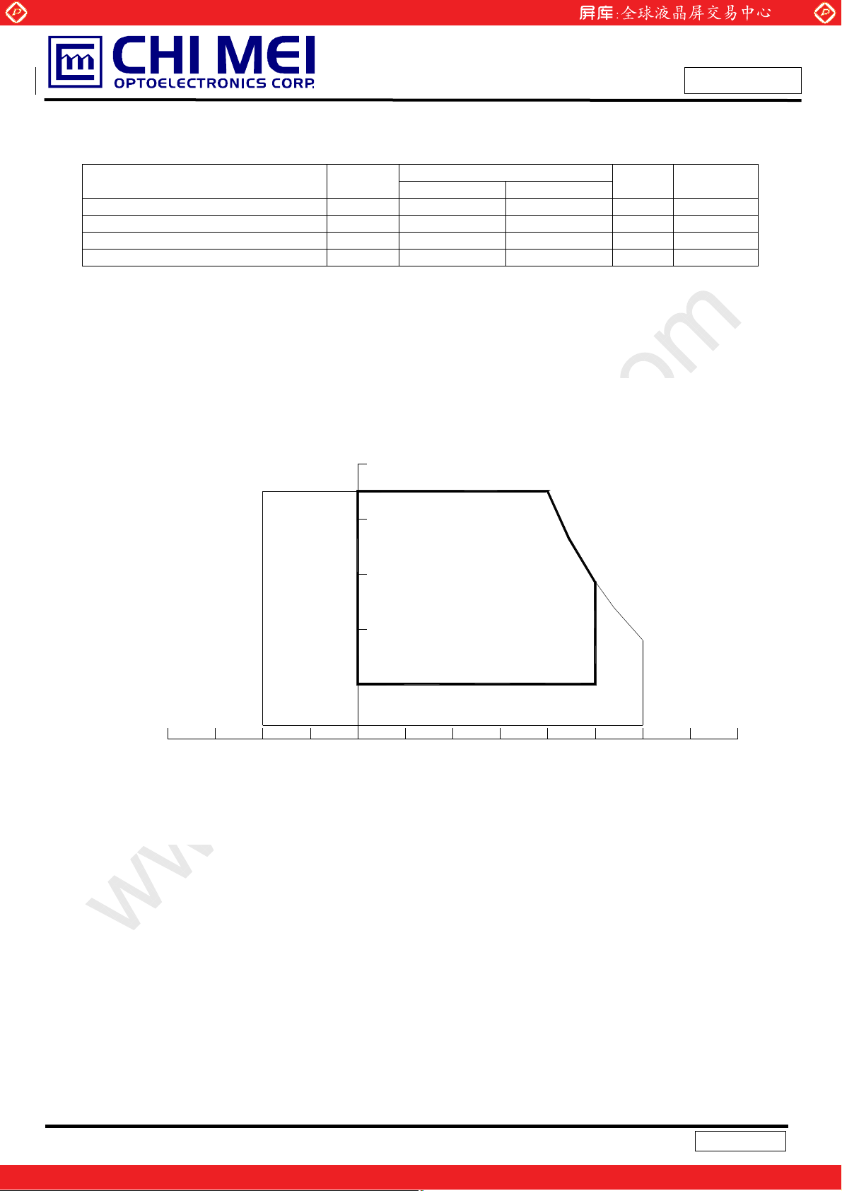
Note (1) Temperature and relative humidity range is shown in the figure below.
(a) 90 %RH Max. (Ta Љ 40 ºC).
(b) Wet-bulb temperature should be 39 ºC Max. (Ta > 40 ºC).
(c) No condensation..
Min. Max.
Value
Unit Note
Preliminary
Relative Humidity (%RH)
100
90
80
60
Operating Range
40
20
10
Storage Range
Temperature (ºC)
80 60 -20 40 0 20 -40
Note (2) The maximum operating temperature is based on the test condition that the surface temperature of
display area is less than or equal to 65 ºC with LCD module alone in a temperature controlled
chamber. Thermal management should be considered in your product design to prevent the surface
temperature of display area from being over 65 ºC. The range of operating temperature may degrade
in case of improper thermal management in your product design.
Note (3) The rating of environment is base on LCD module. Leave LCD cell alone, this environment condition can’t
be guaranteed. Except LCD cell, the customer has to consider the ability of other parts of LCD module
and LCD module process.
5
One step solution for LCD / PDP / OLED panel application: Datasheet, inventory and accessory!
Version 1.0
www.panelook.com
Page 6
Global LCD Panel Exchange Center
www.panelook.com
2.2 ABSOLUTE RATINGS OF ENVIRONMENT (OPEN CELL)
Storage Condition : With shipping package.
Storage temperature range : 25±5 к
Storage humidity range : 50±10%RH
Shelf life : a month
2.3 ELECTRICAL ABSOLUTE RATINGS (OPEN CELL)
VSSD=VSSA=0V
Issued Date: Jun. 17, 2009
Model No.: V460H1-P06
Preliminary
Item
Symbol
Value
Unit
Note
Min Max
Power Supply Voltage
Logic Input Voltage
V
DA
V
GH
V
GL
V
-V
GH
GL
V
DD
-0.5 +18.5 V
-0.3 +43.0 V
-43.0 +0.3 V
-0.3 +43.0 V
-0.3 +5.0 V
(1)
Note (1) Permanent damage to the device may occur if maximum values are exceeded. Function operation
should be restricted to the conditions described under Normal Operating Conditions.
6
One step solution for LCD / PDP / OLED panel application: Datasheet, inventory and accessory!
Version 1.0
www.panelook.com
Page 7
Global LCD Panel Exchange Center
3. ELECTRICAL CHARACTERISTICS
3.1 TFT LCD MODULE
(Ta = 25 ± 2 ºC)
Parameter Symbol
www.panelook.com
Issued Date: Jun. 17, 2009
Model No.: V460H1-P06
Preliminary
Value
Unit Note
Min. Typ. Max.
VGH
Power Supply Voltage
Power Supply Current
CMOS
interface
Note (1) The module should be always operated within the above ranges.
Input High Threshold Voltage VIH 2.7 - 3.3 V
Input Low Threshold Voltage VIL 0 - 0.7 V
VGL
VDA
VDD
IGH
IGL
IAA
IDD
31.5 32 32.5 V
-6.0 -5.5 -5.0 V
17.4 17.7 18.0 V
3.2 3.3 3.4 V
- - 30 mA
- - 50 mA
- - 630 mA
- - 925 mA
3.2 Mini-LVDS CHARACTERISTICS
( Ta = -10~+85 ºC)
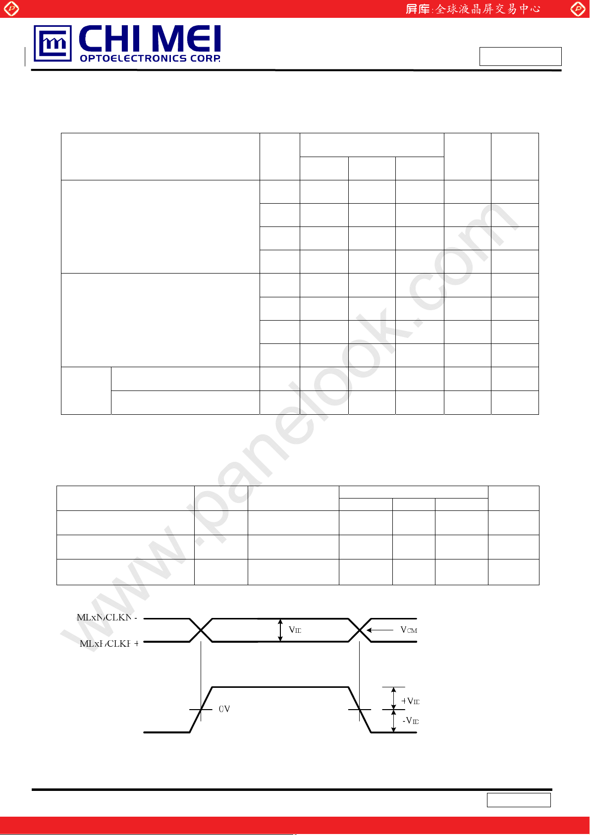
Item Symbol Condition
Mini-LVDS Differential High
Input Voltage
Mini-LVDS Differential Low
Input Voltage
Mini-LVDS common mode
input voltage range
Note (1) VCM= 1.2V (VDD = 3.3V)
+V
-V
V
ID
ID
CM
- 100 - 600 mV
- -600 - -100 mV
- VSSD+0.5 Note(1) VDD-1.2 V
Value
Min Typ Max
Unit
7
One step solution for LCD / PDP / OLED panel application: Datasheet, inventory and accessory!
Version 1.0
www.panelook.com
Page 8
Global LCD Panel Exchange Center
4. BLOCK DIAGRAM OF INTERFACE
4.1 TFT LCD OPEN CELL
www.panelook.com
Issued Date: Jun. 17, 2009
Model No.: V460H1-P06
Preliminary
TFT LCD PANEL
(1920x3x1080)
X(R) Board X(L) Board
Mini-LVDS signal input
CN1 & CN2 Connector, Part NoΚ501559-8010, Molex connector or equivalent
8
One step solution for LCD / PDP / OLED panel application: Datasheet, inventory and accessory!
Version 1.0
www.panelook.com
Page 9

Global LCD Panel Exchange Center
y
y
y
y
y
y
A_
A
y
A
y
y
y
y
y
y
y
y
y
y
y
y
y
y
y
y
y
www.panelook.com
Issued Date: Jun. 17, 2009
Model No.: V460H1-P06
5. INPUT TERMINAL PIN ASSIGNMENT
5.1 TFT LCD Module Input Pin Assignment
CN1(XL) Connector Pin Assignment
Pin No. Symbol Description Pin No. Symbol Description
1 GND Ground 41 GM6 Gamma power suppl
2 N.C. No Connection 42 GM5 Gamma power suppl
3 N.C. No Connection 43 GM4 Gamma power suppl
4 GND Ground 44 GM3 Gamma power suppl
5 N.C. No Connection 45 GM2 Gamma power suppl
6 N.C. No Connection 46 GM1 Gamma power suppl
7 N.C. No Connection 47 GND Ground
8 N.C. No Connection 48 N.C. No Connection
9 N.C. No Connection 49 POL Polarity Control
10 N.C. No Connection 50
11 GND Ground 51 GND Ground
12 ML5N_F mini-LVDS data signal - 52 VD
13 ML5P_F mini-LVDS data signal + 53 VD
14 ML4N_F mini-LVDS data signal - 54 GND Ground
15 ML4P_F mini-LVDS data signal + 55 VDD Driver logic power suppl
16 ML3N_F mini-LVDS data signal - 56 VDD Driver logic power suppl
17 ML3P_F mini-LVDS data signal + 57 GND Ground
18 GND Ground 58 VGH Power supply for Gate on output
19 CLKN_F mini-LVDS clock - 59 VGH Power supply for Gate on output
20 CLKP_F mini-LVDS clock + 60 GND Ground
21 GND Ground 61 N.C. No Connection
22 ML2N_F mini-LVDS data signal - 62 VCM VCM power suppl
23 ML2P_F mini-LVDS data signal + 63 VCM VCM power suppl
24 ML1N_F mini-LVDS data signal - 64 GND Ground
25 ML1P_F mini-LVDS data signal + 65 VGL Power supply for Gate off output
26 ML0N_F mini-LVDS data signal - 66 OE1 Scan driver output enable 1
27 ML0P_F mini-LVDS data signal + 67 CKV Scan driver clock
28 GND Ground 68 STV Scan driver start pulse
29 GM18 Gamma power suppl
30 GM17 Gamma power suppl
31 GM16 Gamma power suppl
32 GM15 Gamma power suppl
33 GM14 Gamma power suppl
34 GM13 Gamma power suppl
35 GM12 Gamma power suppl
36 GM11 Gamma power suppl
37 GM10 Gamma power suppl
38 GM9 Gamma power suppl
39 GM8 Gamma power suppl
40 GM7 Gamma power suppl
69 GND Ground
70 OE2 Scan driver output enable 2
71 N.C. No Connection
72 N.C. No Connection
73 N.C. No Connection
74 N.C. No Connection
75 N.C. No Connection
76 N.C. No Connection
77 N.C. No Connection
78 N.C. No Connection
79 N.C. No Connection
80 GND Ground
TP1 mini-LVDS data latch
Data driver analog power suppl
Data driver analog power suppl
Preliminary
9
One step solution for LCD / PDP / OLED panel application: Datasheet, inventory and accessory!
Version 1.0
www.panelook.com
Page 10

Global LCD Panel Exchange Center
y
y
y
y
y
y
y
y
y
y
y
y
y
t
y
y
t
t
y
y
g
A
y
A
y
y
y
y
y
y
y
CN2(XR) Connector Pin Assignment
Pin No. Symbol Description Pin No. Symbol Description
1 GND Ground 41 GM12 Gamma power suppl
2 VSCM VSCM power suppl
3 N.C. No Connection 43 GM10 Gamma power suppl
4 N.C. No Connection 44 GM9 Gamma power suppl
5 N.C. No Connection 45 GM8 Gamma power suppl
6 N.C. No Connection 46 GM7 Gamma power suppl
7 N.C. No Connection 47 GM6 Gamma power suppl
8 N.C. No Connection 48 GM5 Gamma power suppl
9 N.C. No Connection 49 GM4 Gamma power suppl
10 N.C. No Connection 50 GM3 Gamma power suppl
11 OE2 Scan driver output enable 2 51 GM2 Gamma power suppl
12 GND Ground 52 GM1 Gamma power suppl
13 OE1 Scan driver output enable 1 53 GND Ground
14 CKV Scan driver clock 54 ML5N_B mini-LVDS data signal 15 STV Scan driver start pulse 55 ML5P_B mini-LVDS data signal +
16 VGL Power supply for Gate off outpu
17 GND Ground 57 ML4P_B mini-LVDS data signal +
18 VCM VCM power suppl
19 VCM VCM power suppl
20 N.C. No Connection 60 GND Ground
21 GND Ground 61 CLKN_B mini-LVDS clock 22 VGH Power supply for Gate on outpu
23 VGH Power supplyfor Gate on outpu
24 GND Ground 64 ML2N_B mini-LVDS data signal 25 VDD Driver logic power suppl
26 VDD Driver logic power suppl
27 GND Ground 67 ML1P_Bmini-LVDS data si
28 VD
29 VD
30 GND Ground 70 GND Ground
31 POL Polarity Control 71 N.C. No Connection
32 B_TP1 mini-LVDS data latch 72 N.C. No Connection
33 N.C. No Connection 73 N.C. No Connection
34 GND Ground 74 N.C. No Connection
35 GM18 Gamma power suppl
36 GM17 Gamma power suppl
37 GM16 Gamma power suppl
38 GM15 Gamma power suppl
39 GM14 Gamma power suppl
40 GM13 Gamma power suppl
Note (1) CN1 & CN2 Connector, Part NoΚ501559-8010, Molex connector or equivalent.
Data driver analog power suppl
Data driver analog power suppl
www.panelook.com
Issued Date: Jun. 17, 2009
Model No.: V460H1-P06
42 GM11 Gamma power suppl
56 ML4N_B mini-LVDS data signal -
58 ML3N_B mini-LVDS data signal 59 ML3P_B mini-LVDS data signal +
62 CLKP_B mini-LVDS clock +
63 GND Ground
65 ML2P_B mini-LVDS data signal +
66 ML1N_B mini-LVDS data signal -
68 ML0N_B mini-LVDS data signal 69 ML0P_B mini-LVDS data signal +
75 N.C. No Connection
76 N.C. No Connection
77 GND Ground
78 N.C. No Connection
79 N.C. No Connection
80 GND Ground
Preliminary
nal +
Note (2) The OE1 and OE2 must be connected to the the same OE.
10
One step solution for LCD / PDP / OLED panel application: Datasheet, inventory and accessory!
Version 1.0
www.panelook.com
Page 11

Global LCD Panel Exchange Center
6. INTERFACE TIMING
6.1 INPUT SIGNAL TIMING SPECIFICATIONS
(a) Timing SPEC
Parameter Symbol Condition
Clock period
Clock low pulse width
Clock high pulse width
Data setup time
Data hold time
CLK,LV [5:0] rising time
CLK,LV [5:0] falling time
Start pulse setup time
Start pulse delay time
HD
Reset(RST) high time
TP1 high period
POL to TP1 setup time
www.panelook.com
t
CLK
t
CLK(L)
t
CLK(H)
t
SETUP1
t
HOLD1
t
RISE
t
FALL
t
SETUP2
t
PLH1
t
PHL1
t
RESETH
t
TP1(H)
t
POL-TP1
Loading=15pF - - 13 ns
Loading=15pF - - 13 ns
POL toggle to TP1 rising 5 - - ns
Issued Date: Jun. 17, 2009
Model No.: V460H1-P06
Preliminary
Spec
Unit
Min. Typ. Max.
- 4
- 1.7 - - ns
- 1.7 - - ns
- 0.8 - - ns
- 0.8 - - ns
(1)
- - ns
- - 0.8 ns
- - 0.8 ns
0 - - ns
50ns
over 3
- - -
CLK
200 - - ns
TP1 to POL hold time
Receiver off to TP1 timing
TP1 to reset input time
Reset low to TP1 rising time
t
TP1-POL
t
REC-OFF
t
TP-RESET
t
RESET-TP1
Output delay time1
Output delay time2
Output delay time3
Output delay time4
CKV period
VD
CKV pulse width
OE pulse width
Data setup time
t
CKVH, tCKVL
t
Data hold time
CKV to output delay time
Start pulse output delay time
OE to output delay time
Note (1) : When operation frequency=250MHz
t
PD1
t
PD2
t
PD3
t
PD4
t
CKV
WOE
t
SU
t
HD
t
PD1
t
PD2
t
PD3
TP1 falling to POL toggle 6 - - ns
5 - - CLK
200 - - ns
0 ns
CL=100pF - - 5 ȝs
CL=100pF - - 10 ȝs
CL=100Pf - - 5 ȝs
CL=100pF - - 10 ȝs
- 5 - - ȝs
50% duty cycle 2.5 - - ȝs
- 1 - - ȝs
0.5 - - ȝs
0.5 - - ȝs
CL=300pF - - 1 ȝs
- CL=300pF - - 0.8 ȝs
CL=300pF - - 0.8 ȝs
11
One step solution for LCD / PDP / OLED panel application: Datasheet, inventory and accessory!
Version 1.0
www.panelook.com
Page 12

Global LCD Panel Exchange Center
(b) Horizontal Timing Chart
www.panelook.com
Issued Date: Jun. 17, 2009
Model No.: V460H1-P06
Preliminary
Last data sampling to TP1 timing for 726 channel caseΚΚΚΚ
12
Version 1.0
One step solution for LCD / PDP / OLED panel application: Datasheet, inventory and accessory!
www.panelook.com
Page 13

Global LCD Panel Exchange Center
www.panelook.com
Issued Date: Jun. 17, 2009
Model No.: V460H1-P06
Preliminary
Relationship between EIO (OUT) and EIO (IN) timing for 726 channel caseΚΚΚΚ
13
One step solution for LCD / PDP / OLED panel application: Datasheet, inventory and accessory!
Version 1.0
www.panelook.com
Page 14

Global LCD Panel Exchange Center
(C) Vertical Timing Chart
www.panelook.com
Issued Date: Jun. 17, 2009
Model No.: V460H1-P06
Preliminary
14
One step solution for LCD / PDP / OLED panel application: Datasheet, inventory and accessory!
Version 1.0
www.panelook.com
Page 15

Global LCD Panel Exchange Center
6.2 POWER ON/OFF SEQUENCE
To prevent the device from damage due to latch up , the power ON/OFF sequence shown below must be
followed.
When power onΚVDD ĺ VGL ĺ VDA ĺ VGH (t1Ї0)
When power offΚVGH ĺ VDA ĺ VGL ĺ VDD (t2 0)Њ
www.panelook.com
Issued Date: Jun. 17, 2009
Model No.: V460H1-P06
Preliminary
VGH
VDA
VDD
VSSD,VSSA
t
t1 t2
VGL
15
One step solution for LCD / PDP / OLED panel application: Datasheet, inventory and accessory!
Version 1.0
www.panelook.com
Page 16

Global LCD Panel Exchange Center
7. OPTICAL CHARACTERISTICS
7.1 TEST CONDITIONS
Item Symbol Value Unit
Ambient Temperature Ta
Ambient Humidity Ha
Supply Voltage V
Input Signal According to typical value in "3. ELECTRICAL CHARACTERISTICS"
Lamp Current I
Oscillating Frequency (Inverter) F
Vertical Frame Rate Fr 60 Hz
7.2 OPTICAL SPECIFICATIONS
The relative measurement methods of optical characteristics are shown in 7.2. The following items should be
www.panelook.com
CC
L
W
10.50.3
Issued Date: Jun. 17, 2009
Model No.: V460H1-P06
252
5010
12V V
463
Preliminary
o
C
%RH
mA
KHz
measured under the test conditions described in 7.1 and stable environment shown in Note (6).
Item Symbol Condition Min. Typ. Max. Unit Note
Contrast Ratio CR 3800 5000 - - Note (2)
Gray to
Response Time
- 6.5 12 ms Note (3)
gray
cd/
Center Luminance of White L
White Variation
C
W
450 500 -
m
2
Note (4)
- - 1.3 - Note (7)
Cross Talk CT - - 4 % Note (5)
=0, Y =0
Red
Rx 0.634 -
Ry
x
Viewing angle at
0.323
-
normal direction
Gx 0.287 -
Green
0.602
0.056
0.280
Typ.+
0.03
Note (6)
-
-
Color
Chromaticity
Blue
Gy
Bx 0.148 -
Typ.-
0.03
By
Wx
White
Wy
0.290
-
Color Gamut
x+
72 - % NTSC
80 88 -
Horizontal
Viewing
-
x
80 88 -
CR20
Angle
Y+
80 88 -
Vertical
-
Y
80 88 -
16
One step solution for LCD / PDP / OLED panel application: Datasheet, inventory and accessory!
Deg. Note (1)
Version 1.0
www.panelook.com
Page 17

Global LCD Panel Exchange Center
T
Note (1) Definition of Viewing Angle (x, y):
Viewing angles are measured by Eldim EZ-Contrast 160R
www.panelook.com
Issued Date: Jun. 17, 2009
Model No.: V460H1-P06
Preliminary
Normal
x = y = 0º
y- y
X- = 90º
x-
x
6 o’clock
y-
= 90º
y-
Note (2) Definition of Contrast Ratio (CR):
The contrast ratio can be calculated by the following expression.
Contrast Ratio (CR) = L255 / L0
L255: Luminance of gray level 255
L 0: Luminance of gray level 0
CR = CR (5), where CR (X) is corresponding to the Contrast Ratio of the point X at the figure in Note (7)
Note (3) Definition of Gray to Gray Switching Time :
x
y+
12 o’clock direction
y+
= 90º
x+
X+ = 90º
100%
90%
Optical
Response
10%
0%
Gray to gray
switching time
Gray to gray
switching time
ime
The driving signal means the signal of luminance 0%, 20%, 40%, 60%, 80%, 100%.
Gray to gray average time means the average switching time of luminance 0%,20%, 40%, 60%, 80%, 100% to
each other.
17
Version 1.0
One step solution for LCD / PDP / OLED panel application: Datasheet, inventory and accessory!
www.panelook.com
Page 18

Global LCD Panel Exchange Center
A
(
)
A
(
)
(
)
Note (4) Definition of Luminance of White (LC):
Measure the luminance of gray level 255 at center point.
L
= L (5), where L (x) is corresponding to the luminance of the point X at the figure in Note (7).
C
Note (5) Definition of Cross Talk (CT):
www.panelook.com
Issued Date: Jun. 17, 2009
Model No.: V460H1-P06
Preliminary
Y
(D/8,W/2)
A, L
Y
(D/2,7W/8)
A, D
CT = | Y
Where:
(0, 0)
– YA | / YA 100 (%)
B
Y
= Luminance of measured location without gray level 51 pattern (cd/m2)
A
Y
= Luminance of measured location with gray level 255 pattern (cd/m2)
B
ctive Area
Gray 0
Y
Y
A, R
D, W
A, U
(D/2,W /8)
(7D/8,W/2)
(D/4,W/4)
(D/8,W/2)
Y
B, L
Y
(D/2,7W/8)
B, D
0, 0
ctive Area
Gray 0
Y
(D/2,W /8)
B, U
Y
B, R
(3D/4,3W/4)
D, W
(7D/8,W/2)
18
One step solution for LCD / PDP / OLED panel application: Datasheet, inventory and accessory!
Version 1.0
www.panelook.com
Page 19

Global LCD Panel Exchange Center
Note (6) Measurement Setup:
The LCD module should be stabilized at given temperature for 1 hour to avoid abrupt temperature
change during measuring. In order to stabilize the luminance, the measurement should be executed
after lighting backlight for 1 hour in a windless room.
LCD Module
LCD Panel
www.panelook.com
Issued Date: Jun. 17, 2009
Model No.: V460H1-P06
Preliminary
Center of the Screen
Note (7) Definition of White Variation (W):
Measure the luminance of gray level 1023 at 5 points
W = Maximum [L (1), L (2), L (3), L (4), L (5)] / Minimum [L (1), L (2), L (3), L (4), L (5)]
Display Color Analyzer
(Minolta CA210)
Light Shield Room
(Ambient Luminance < 2 lux)
Horizontal Line
D
Vertical Line
W
W/4
W/2
3W /4
D/4 D/2 3D/4
1 2
5
3 4
Active Area
19
X
: Test Point
X=1 to 5
Version 1.0
One step solution for LCD / PDP / OLED panel application: Datasheet, inventory and accessory!
www.panelook.com
Page 20

Global LCD Panel Exchange Center
8. DEFINITION OF LABELS
8.1 OPEN CELL LABEL
The barcode nameplate is pasted on each open cell as illustration for CMO internal control.
8.2 CARTON LABEL
The barcode nameplate is pasted on each box as illustration, and its definitions are as following explanation
www.panelook.com
Issued Date: Jun. 17, 2009
Model No.: V460H1-P06
Preliminary
-
XXXXXXXXXXXXXX
(a) Model Name: V460H1– P06
P.O. NO.
Parts ID.
Carton ID. Quantities 8
XXXXXXXXXXXXXX
Made in Taiwan
(b) Carton ID: CMO internal control
(c) Quantities: 8
20
One step solution for LCD / PDP / OLED panel application: Datasheet, inventory and accessory!
Version 1.0
www.panelook.com
Page 21

Global LCD Panel Exchange Center
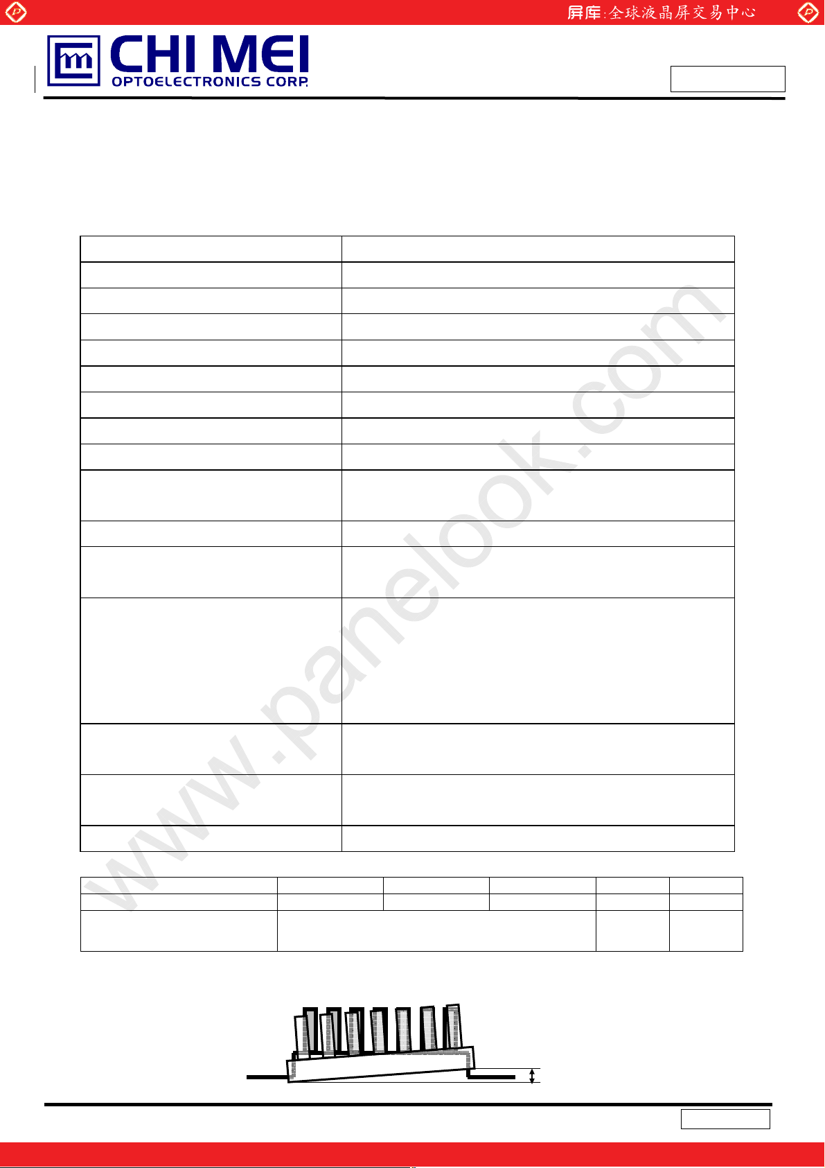
9. PACKAGING
9.1 PACKING SPECIFICATIONS
(1) 8 LCD TV Panels / 1 Box
(2) Box dimensions :1238 (L) X 842 (W) X 240(H)
(3) Weight : approximately 38Kg (8 panels per box)
9.2 PACKING METHOD
Figures 9-1 and 9-2 are the packing method
www.panelook.com
Issued Date: Jun. 17, 2009
Model No.: V460H1-P06
Preliminary
Figure.9-1 packing method
21
One step solution for LCD / PDP / OLED panel application: Datasheet, inventory and accessory!
Version 1.0
www.panelook.com
Page 22

Global LCD Panel Exchange Center
www.panelook.com
Issued Date: Jun. 17, 2009
Model No.: V460H1-P06
Preliminary
Figure.9-2 packing method
22
One step solution for LCD / PDP / OLED panel application: Datasheet, inventory and accessory!
Version 1.0
www.panelook.com
Page 23

Global LCD Panel Exchange Center
www.panelook.com
Issued Date: Jun. 17, 2009
Model No.: V460H1-P06
Preliminary
10. PRECAUTIONS
10.1 ASSEMBLY AND HANDLING PRECAUTIONS
(1) Do not apply rough force such as bending or twisting to the product during assembly.
(2) To assemble backlight or install module into user’s system can be only in clean working areas. The dust
and oil may cause electrical short or worsen the polarizer.
(3) It’s not permitted to have pressure or impulse on the module because the LCD panel will be damaged.
(4) Always follow the correct power sequence when the product is connecting and operating. This can
prevent damage to the CMOS LSI chips during latch-up.
(5) Do not pull the I/F connector in or out while the module is operating.
(6) Use a soft dry cloth without chemicals for cleaning, because the surface of polarizer is very soft and easily
scratched.
(7) It is dangerous that moisture come into or contacted the product, because moisture may damage the
product when it is operating.
(8) High temperature or humidity may reduce the performance of module. Please store this product within the
specified storage conditions.
(9) When ambient temperature is lower than 10ºC may reduce the display quality. For example, the response
time will become slowly.
10.2 SAFETY PRECAUTIONS
(1) If the liquid crystal material leaks from the panel, it should be kept away from the eyes or mouth. In case
of contact with hands, skin or clothes, it has to be washed away thoroughly with soap.
(2) After the product’s end of life, it is not harmful in case of normal operation and storage.
23
One step solution for LCD / PDP / OLED panel application: Datasheet, inventory and accessory!
Version 1.0
www.panelook.com
Page 24

Global LCD Panel Exchange Center
11. Mechanical Drawing
www.panelook.com
Issued Date: Jun. 17, 2009
Model No.: V460H1-P06
Preliminary
ڻႝηިҽԖ Ϧљ
24
One step solution for LCD / PDP / OLED panel application: Datasheet, inventory and accessory!
Version 1.0
www.panelook.com
Page 25

Global LCD Panel Exchange Center
www.panelook.com
Issued Date: Jun. 17, 2009
Model No.: V460H1-P06
Preliminary
ڻႝηިҽԖϦљ
25
One step solution for LCD / PDP / OLED panel application: Datasheet, inventory and accessory!
Version 1.0
www.panelook.com
 Loading...