

Page 1
Global LCD Panel Exchange Center
TFT LCD Approval Specification
MODEL NO.: V420H1 – PH5
Customer: _________________________________
Approved by:_______________________________
www.panelook.com
Issue Date:Aug.24.2009
Model No.: V420H1-PH5
Preliminary
Note:
TV Head Division
Approved By
Chao-Chun Chung
Reviewed By
QA Dept. Product Development Div.
Hsin-Nan Chen WT Lin
Prepared By
LCD TV Marketing and Product Management Div.
CY Chang Justin Wang
1
One step solution for LCD / PDP / OLED panel application: Datasheet, inventory and accessory!
Version 1.0
www.panelook.com
Page 2

Global LCD Panel Exchange Center
www.panelook.com
Issue Date:Aug.24.2009
Model No.: V420H1-PH5
Preliminary
CONTENTS
REVISION HISTORY ..................................................................................................................................................4
1. GENERAL DESCRIPTION......................................................................................................................................5
1.1 OVERVIEW....................................................................................................................................................5
1.2 FEATURES....................................................................................................................................................5
1.3 APPLICATION ...............................................................................................................................................5
1.4 GENERAL SPECIFICATIONS........................................................................................................................5
1.5 MECHANICAL SPECIFICATIONS .................................................................................................................6
2. ABSOLUTE MAXIMUM RATINGS ...........................................................................................................................7
2.1 ABSOLUTE RATINGS OF ENVIRONMENT...................................................................................................7
2.2 PACKAGE STORAGE ...................................................................................................................................7
2.3 ELECTRICAL ABSOLUTE RATINGS ............................................................................................................8
2.3.1 TFT LCD MODULE..............................................................................................
2.3.2 BACKLIGHT INVERTER UNIT ............................................................................
3. ELECTRICAL CHARACTERISTICS ........................................................................................................................9
ᙑᎄ
ᙑᎄ! ࡸآࡳᆠ᧘
ࡸآࡳᆠ᧘ΖΖΖΖ
ᙑᎄᙑᎄ
ࡸآࡳᆠ᧘ࡸآࡳᆠ᧘
ᙑᎄ
ᙑᎄ! ࡸآࡳᆠ᧘
ࡸآࡳᆠ᧘ΖΖΖΖ
ᙑᎄᙑᎄ
ࡸآࡳᆠ᧘ࡸآࡳᆠ᧘
3.1 TFT LCD MODULE........................................................................................................
3.2 BACKLIGHT CONNECTOR PIN CONFIGURATION ....................................................
3.2.1 LAMP SPECIFICATION................................................................................................................ … .12
3.2.2 ELECTRICAL SPECIFICATION........................................................................
3.2.3 INVERTER INTERFACE CHARACTERISTICS............................................................. ……………. 14
4. BLOCK DIAGRAM OF INTERFACE................................................................................................. …… 110
4.1 TFT LCD MODULE........................................................................................................
5. INPUT TERMINAL PIN ASSIGNMENT .................................................................................................................. 11
5.1 TFT LCD Module Input ...............................................................................................................................11
5.2 BACKLIGHT UNIT .......................................................................................................................................12
5.3 INVERTER UNIT............................................................................................................
5.4 BLOCK DIAGRAM OF INTERFACE ............................................................................................................15
5.5 LVDS INTERFACE.......................................................................................................................................17
5.6 COLOR DATA INPUT ASSIGNMENT...........................................................................................................18
ᙑᎄ! ࡸآࡳᆠ᧘Ζ
ᙑᎄ! ࡸآࡳᆠ᧘Ζ
ᙑᎄ
ᙑᎄ! ࡸآࡳᆠ᧘
ࡸآࡳᆠ᧘ΖΖΖΖ
ᙑᎄᙑᎄ
ࡸآࡳᆠ᧘ࡸآࡳᆠ᧘
ᙑᎄ! ࡸآࡳᆠ᧘Ζ
ᙑᎄ! ࡸآࡳᆠ᧘Ζ
2
2
6. INTERFACE TIMING.............................................................................................................................................19
6.1 INPUT SIGNAL TIMING SPECIFICATIONS ................................................................................................. 19
2
One step solution for LCD / PDP / OLED panel application: Datasheet, inventory and accessory!
Version 1.0
www.panelook.com
Page 3
Global LCD Panel Exchange Center
6.2 POWER ON/OFF SEQUENCE.................................................................................
www.panelook.com
Issue Date:Aug.24.2009
Model No.: V420H1-PH5
Preliminary
ᙑᎄ! ࡸآࡳᆠ᧘Ζ
7. OPTICAL CHARACTERISTICS.............................................................................................................................19
7.1 TEST CONDITIONS.....................................................................................................................................22
7.2 OPTICAL SPECIFICATIONS .......................................................................................................................23
8. PRECAUTIONS ....................................................................................................................................................26
8.1 ASSEMBLY AND HANDLING PRECAUTIONS............................................................................................ 26
8.2 SAFETY PRECAUTIONS.............................................................................................................................26
9. DEFINITION OF LABELS......................................................................................................................................27
9.1 CMO MODULE LABEL................................................................................................................................ 27
10. PACKAGING.......................................................................................................................................................28
10.1 PACKAGING SPECIFICATIONS................................................................................................................ 28
10.2 PACKAGING METHOD................................................................................................
11. MECHANICAL CHARACTERISTICS ...................................................................................................................30
ᙑᎄ! ࡸآࡳᆠ᧘Ζ
3
One step solution for LCD / PDP / OLED panel application: Datasheet, inventory and accessory!
Version 1.0
www.panelook.com
Page 4
Global LCD Panel Exchange Center
play
REVISION HISTORY
Version Date Page(New) Section Description
Ver. 0.0 Oct. 15, 2008 All All The tentative specification was first issued.
Ver. 1.0 Dec. 19, 2008 5 1.2 Revised fast response time
6 1.5 Revised weight
9 3.1 Updated TFT LCD module parameter
11 3.2.1 Updated Lamp specification
11-12 3.2.2 Updated BL electrical specification
13 3.2.3 Updated inverter interface characteristics
16-17 5.1 Updated TFT LCD module input
18-19 5.3 Updated inverter unit
24 6.1 Updated input signal timing specifications
26 6.2 Updated Power ON/OFF sequence
29 7.2 Updated optical specifications
34-35 10 Updated packing
36-38 11 Updated mechanical characteristics
Ver. 1.0 Dec. 23, 2008 18 5.3 Updated inverter pin 12 define
Ver. 1.0 Dec. 24, 2008 5 1.1 Modified “8-bit + FRC” to “10-bit”
29-31 7.2 Updated Center Luminance of White spec
Ver. 1.1 Dec. 31, 2008 13 3.2.3 Add note(4)
14 3.2.3 Updated power sequence and control signal timing fig.
17 5.1 Updated pin define
Ver. 2.0 Feb. 12. 2009 11
16
17-19
29
30
35
35
37-39
Ver. 2.1
Apr. 8, 2009 13
13
14
15
26
38
www.panelook.com
3.2.1
3.2.2
5.1
5.1
7.1
7.2
10.1
10.2
11
3.2.3
3.2.3
3.2.3
4.1
6.1
11
Updated BLU connector pin configure.
Updated BLU connector pin configure.
Updated TFT LCD Module Input
Updated LVDS pin assignment.
Updated optical measurement condition.
Updated optical specification.
Updated package specification.
Updated package specification.
Updated ME specification.
Modified Internal PWM Control Voltage Max. value
Deleted Note 4
Modified the V
Modified the Block Diagram of the BLU
Modified Vertical Active Dis
Display Term
Modified Mechanical Characteristics (Removed FFC)
IPWM
Issue Date:Aug.24.2009
Model No.: V420H1-PH5
Preliminary
value
Term and Horizontal Active
Ver. 2.2 Apr. 18, 2009 11
13
14
Ver. 2.3 Apr. 23, 2009 13
25
Ver. 2.4 Jun. 4, 2009 30 7.1 Modified Oscillating Frequency
Ver. 2.5 Aug. 6,2009 9-11
16
17-19
28
40-47
35-36
3.2.2
3.2.3
3.2.3
3.2.3
6.1
3.1
4.1
5.1
6.2
Appendix
10
Updated Max Values of Power Consumption
Deleted Max Values of VBL Rising/Falling Time, PWM
Delay Time, BLON Delay Time, and BLON Off Time
IPWM
Modified the V
Modified BLON Delay Time and BLON Off Time
Updated Frame Rate
TFT LCD MODULE
TFT LCD MODULE
TFT LCD Module Input
POWER ON/OFF SEQUENCE
Add Appendix
PACKAGING
value
4
One step solution for LCD / PDP / OLED panel application: Datasheet, inventory and accessory!
Version 1.0
www.panelook.com
Page 5
Global LCD Panel Exchange Center
1. GENERAL DESCRIPTION
1.1 OVERVIEW
V420H1-PH5 is a 42” TFT Liquid Crystal Display module with driver ICs and 2ch-LVDS interface. This
module supports 1920 x 1080 Full HDTV format and can display 1.07G colors (10-bit/color). The backlight
unit is not built-in.
1.2 FEATURES
Ё
High contrast ratio (4000:1)
Ё
Fast response time (Gray to gray average 4.0 ms)
Ё
High color saturation (NTSC 72%)
Ё
Full HDTV (1920 x 1080 pixels) resolution, true HDTV format
Ё
DE (Data Enable) only mode
www.panelook.com
Issue Date:Aug.24.2009
Model No.: V420H1-PH5
Preliminary
Ё
LVDS (Low Voltage Differential Signaling) interface
Ё
Optimized response time for 120 Hz frame rate with MEMC
Ё
Ultra wide viewing angle : Super MVA technology
Ё
RoHS compliance
1.3 APPLICATION
Ё
Standard Living Room TVs.
Ё
Public Display Application.
Ё
Home Theater Application.
Ё
MFM Application.
1.4 GENERAL SPECIFICATIONS
Item Specification Unit Note
Active Area 930.24(H) x 523.26 (V) (42.02” diagonal) mm
Bezel Opening Area 937.24 (H) x 530.26 (V) mm
Driver Element a-si TFT active matrix - -
Pixel Number 1920 x R.G.B. x 1080 pixel -
(1)
Pixel Pitch(Sub Pixel) 0.1615 (H) x 0.4845 (V) mm -
Pixel Arrangement RGB vertical stripe - -
Display Colors 1.07G color -
Display Operation Mode Transmissive mode / Normally black - -
Surface Treatment
Note (1) Please refer to the attached drawings in chapter 9 for more information about the front and back outlines.
Note (2) The spec. of the surface treatment is temporarily for this phase. CMO reserves the rights to change this
feature.
Anti-Glare coating (Haze 11%)
Hard coating (3H)
- (2)
5
One step solution for LCD / PDP / OLED panel application: Datasheet, inventory and accessory!
Version 1.0
www.panelook.com
Page 6
Global LCD Panel Exchange Center
1.5 MECHANICAL SPECIFICATIONS
Item Min. Typ. Max. Unit Note
Weight 2100 2150 2200 g -
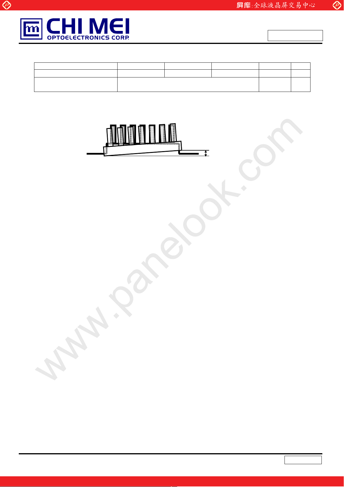
I/F connector mounting position
Note (1) Please refer to the attached drawings for more information of front and back outline dimensions.
Note (2) Connector mounting position
www.panelook.com
The mounting inclination of the connector makes the
screen center within
0.5mm as the horizontal.
+/- 0.5mm
Issue Date:Aug.24.2009
Model No.: V420H1-PH5
Preliminary
(2)
6
One step solution for LCD / PDP / OLED panel application: Datasheet, inventory and accessory!
Version 1.0
www.panelook.com
Page 7
Global LCD Panel Exchange Center
2. ABSOLUTE MAXIMUM RATINGS
www.panelook.com
Issue Date:Aug.24.2009
Model No.: V420H1-PH5
Preliminary
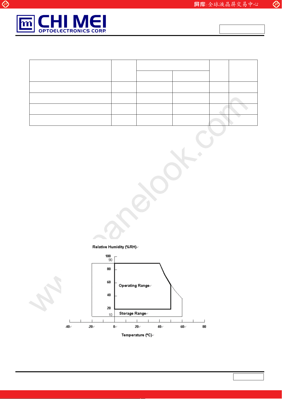
2.1 ABSOLUTE RATINGS OF ENVIRONMENT
Item Symbol
Storage Temperature TST -20 +60 ºC (1)
Operating Ambient Temperature TOP 0 50 ºC (1), (2)
Shock (Non-Operating) SNOP - 50 G (3), (5)
Vibration (Non-Operating) VNOP - 1.0 G (4), (5)
Note (1) Temperature and relative humidity range is shown in the figure below.
(a) 90 %RH Max. (Ta
(b) Wet-bulb temperature should be 39 ºC Max. (Ta > 40 ºC).
(c) No condensation.
Note (2) The maximum operating temperature is based on the test condition that the surface temperature of
display area is less than or equal to 65 ºC with LCD module alone in a temperature controlled chamber.
Thermal management should be considered in final product design to prevent the surface temperature of
display area from being over 65 ºC. The range of operating temperature may degrade in case of
Љ
40 ºC).
(BASE ON CMO MODULE V420H1-LH5)
Value
Min. Max.
Unit Note
improper thermal management in final product design.
Note (3) 11 ms, half sine wave, 1 time for ± X, ± Y, ± Z.
Note (4) 10 ~ 200 Hz, 10 min, 1 time each X, Y, Z.
Note (5) At testing Vibration and Shock, the fixture in holding the module has to be hard and rigid enough so that
the module would not be twisted or bent by the fixture.
7
One step solution for LCD / PDP / OLED panel application: Datasheet, inventory and accessory!
Version 1.0
www.panelook.com
Page 8
Global LCD Panel Exchange Center
www.panelook.com
2.2 ABSOLUTE RATINGS OF ENVIRONMENT (OPEN CELL)
Storage condition: With shipping package.
Issue Date:Aug.24.2009
Model No.: V420H1-PH5
Preliminary
Storage temperature rang: 25
Storage humidity range: 50
Shelf life: a month
2.3 ELECTRICAL ABSOLUTE RATINGS
2.3.1 ELECTRICAL ABSOLUTE RATINGS (OPEN CELL)
Item Symbol
Power Supply Voltage VAA -0.5 +18 V
Power Supply Voltage VGH -0.3 +32.3 V
Power Supply Voltage VGL -5.7 -0.3 V
Logic Input Voltage VDD -0.3 3.4 V
Note (1) Permanent damage to the device may occur if maximum values are exceeded. Function operation
should be restricted to the conditions described under Normal Operating Conditions.
5к
10%RH
Value
Unit Note
Min. Max.
(1)
8
One step solution for LCD / PDP / OLED panel application: Datasheet, inventory and accessory!
Version 1.0
www.panelook.com
Page 9
Global LCD Panel Exchange Center
3. ELECTRICAL CHARACTERISTICS
3.1 TFT LCD MODULE
(Ta = 25 ± 2 ºC)
Parameter Symbol
www.panelook.com
Issue Date:Aug.24.2009
Model No.: V420H1-PH5
Preliminary
Value
Unit Note
Min. Typ. Max.
VGH 31 32 33 V
VGL -5.8 -5.5 -5.2 V
Power Supply Voltage
VAA 15.9 16.2 16.5 V
VDD 3.2 3.3 3.4 V
V
15.17 15.47 15.77 V
REF
IGH - 31.49 40.3 mA
IGL - 7.73 10.79 mA
Power Supply Current
IAA - 627 890.5 mA
I
1.41 1.84 A
DD
CMOS
interface
Input High Threshold Voltage VIH 2.7 - 3.3 V
Input Low Threshold Voltage V
0 - 0.7 V
IL
Note (1) The module should be always operated within the above ranges.
3.2
RSDS CHARACTERISTICS
VDDD=3.0 to 3.6V, VDDA=13.5 to 18.0V, VSSD=VSSA=0V, Ta = -20~+85 ºC
Item Symbol Condition
RSDS high input Voltage V
RSDS low input Voltage V
RSDS common mode
input voltage range
RSDS Input leakage
current
DIFFRSDSVCMRSDS
DIFFRSDSVCMRSDS
V
V
CMRSDS
I
DL
DIFFRSDS
A/BDxxP, A/BDxxN,
A/BCLKP, A/BCLKN
= +1.2 V (1) 100 200 600
= +1.2 V (1) -600 -200 -100
= 200 mV
(2)
Min Typ Max
VSSD+0.5 Note(3) VDDD-1.2 V
-10 - 10
Value
Unit
mV
Ӵ
A
Note (1) V
Note (2) V
Note (3) V
= (VCLKP + VCLKN)/2 or V
CMRSDS
DIFFRSDS
= VCLKP - VCLKN or V
= 1.2V(VDDD = 3.3V)
CMRSDS
CMRSDS
DIFFRSDS
= (VDXXP + VDXXN)/2
= VDXXP - VDXXN
9
One step solution for LCD / PDP / OLED panel application: Datasheet, inventory and accessory!
Version 1.0
www.panelook.com
Page 10
Global LCD Panel Exchange Center
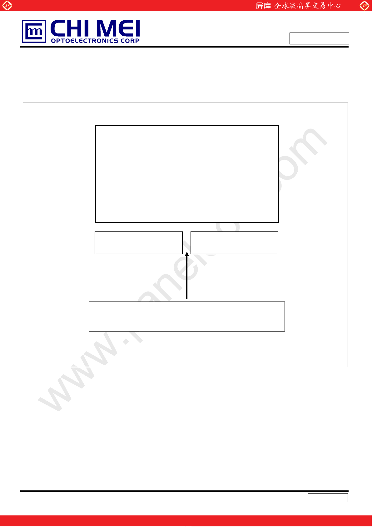
4. BLOCK DIAGRAM OF INTERFACE
4.1 TFT LCD OPEN CELL
www.panelook.com
Issue Date:Aug.24.2009
Model No.: V420H1-PH5
Preliminary
TFT LCD PANEL
(1920x3x1080)
X(R) Board X(L) Board
RSDS Signal Input
10
One step solution for LCD / PDP / OLED panel application: Datasheet, inventory and accessory!
Version 1.0
www.panelook.com
Page 11
Global LCD Panel Exchange Center
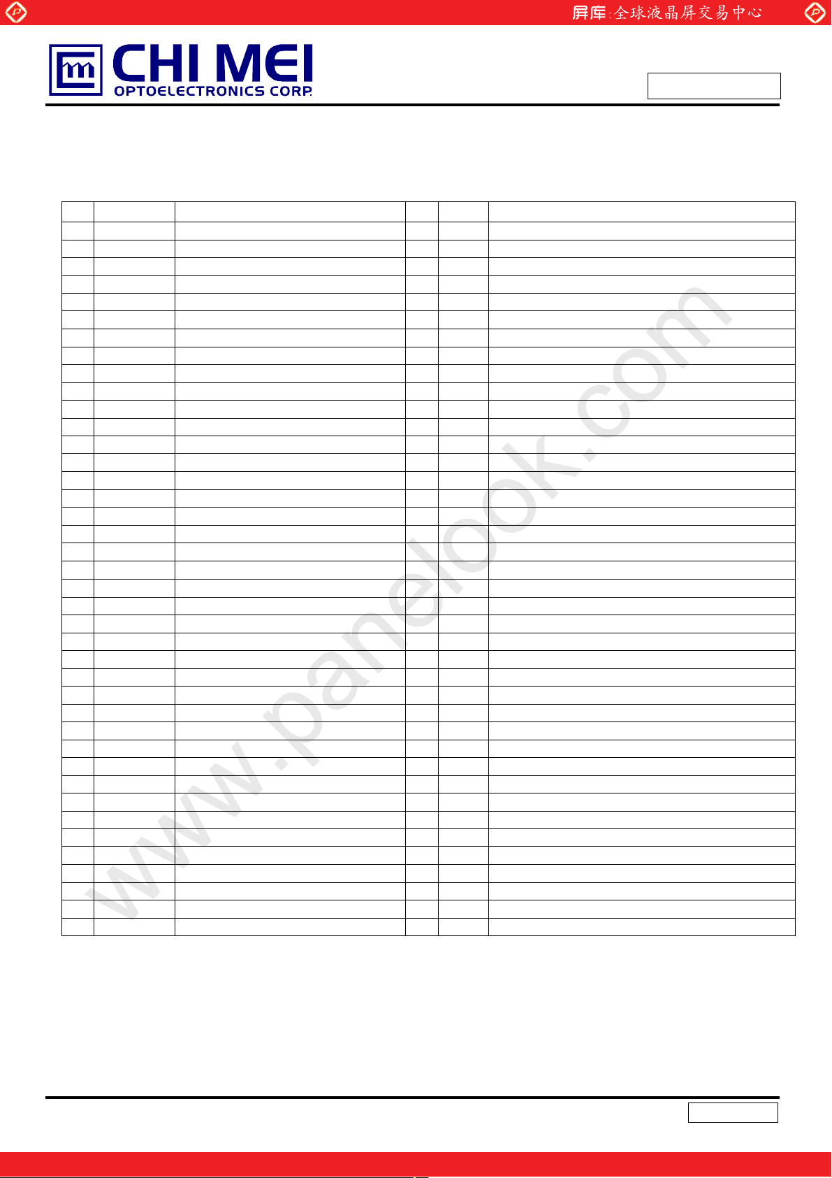
5. INPUT TERMINAL PIN ASSIGNMENT
5.1 TFT LCD Module Input
www.panelook.com
Issue Date:Aug.24.2009
Model No.: V420H1-PH5
Preliminary
CNX1(XL) Connector Pin Assignment
Pin Symbol Description Pin Symbol Description
1 GND
2 NC No connection 42 GM5
3 NC No connection 43 GM4
4 NC No connection 44 GM3
5 NC No connection 45 GM2
6 TP1
7 NC No connection 47 GND
8 CKV
9STV
10 OE1
11 O E2
12 NC No connection 52 VGL
13 V33L
14 V33L
15 NC No connection 55 GND
16 NC No connection
17 NC No connection
18 NC No connection
19 GND
20 VCS Charge sharing trace
21 VCS Charge sharing trace
22 VCS Charge sharing trace
23 VCS Charge sharing trace
24 VCS Charge sharing trace
25 VCS Charge sharing trace
26 GND
27 GM20
28 GM19
29 GM18
30 GM17
31 GM16
32 GM15
33 GM14
34 GM13
35 GM12
36 GM11
37 GM10
38 GM9
39 GM8
40 GM7
Scan driver start pulse
Scan driver output1 enable
Scan driver output2 enable
Gamma Power supply
Gamma Power supply
Gamma Power supply
Gamma Power supply
Gamma Power supply
Gamma Power supply
Gamma Power supply
Gamma Power supply
Gamma Power supply
Gamma Power supply
Gamma Power supply
Gamma Power supply
Gamma Power supply
Gamma Power supply
Ground
RSDS data latch
Scan driver clock
Logic Power supply
Logic Power supply
Ground
Ground
41 GM6
46 GM1
48 VCM VCM Power supply
49 VCM VCM Power supply
50 VAA
51 VAA
53 NC No connection
54 VGH
Gamma Power supply
Gamma Power supply
Gamma Power supply
Gamma Power supply
Gamma Power supply
Gamma Power supply
Ground
Driver Power supply
Driver Power supply
Driver Power supply
Driver Power supply
Ground
11
One step solution for LCD / PDP / OLED panel application: Datasheet, inventory and accessory!
Version 1.0
www.panelook.com
Page 12
Global LCD Panel Exchange Center
CNX2(XL) Connector Pin Assignment
Pin Symbol Description Pin Symbol Description
1 GND
2 BD1P_6
3 BD1M_6
4 BD0P_6
5 BD0M_6
6 AD1P_6
7 AD1M_6
8 AD0P_6
9 AD0M_6
10 BD1P_5
11 BD1M_5
12 BD0P_5
13 BD0M_5
14 AD1P_5
15 AD1M_5
16 AD0P_5
17 AD0M_5
18 BD1P_4
19 BD1M_4
20 BD1P_4
21 BD0M_4
22 BD0P_4
23 AD1P_4
24 AD1M_4
25 AD0P_4
26 AD0M_4
27 BD1P_3
28 BD1M_3
29 BD0P_3
30 BD0M_3
31 AD1P_3
32 AD1M_3
33 AD0P_3
34 GND
35 B_CLKP
36 B_CLKM
37 BD1P_2
38 BD1M_2
39 BD0P_2
40 BD0M_2
B-Path RSDS data signal
B-Path RSDS data signal
B-Path RSDS data signal
B-Path RSDS data signal
A-Path RSDS data signal
A-Path RSDS data signal
A-Path RSDS data signal
A-Path RSDS data signal
B-Path RSDS data signal
B-Path RSDS data signal
B-Path RSDS data signal
B-Path RSDS data signal
A-Path RSDS data signal
A-Path RSDS data signal
A-Path RSDS data signal
A-Path RSDS data signal
B-Path RSDS data signal
B-Path RSDS data signal
B-Path RSDS data signal
B-Path RSDS data signal
B-Path RSDS data signal
A-Path RSDS data signal
A-Path RSDS data signal
A-Path RSDS data signal
A-Path RSDS data signal
B-Path RSDS data signal
B-Path RSDS data signal
B-Path RSDS data signal
B-Path RSDS data signal
A-Path RSDS data signal
A-Path RSDS data signal
A-Path RSDS data signal
B-Path Data driver clock
B-Path Data driver clock
B-Path RSDS data signal
B-Path RSDS data signal
B-Path RSDS data signal
B-Path RSDS data signal
Ground
Ground
www.panelook.com
Issue Date:Aug.24.2009
Model No.: V420H1-PH5
41 A_CLKP
42 A_CLKM
43 AD1P_2
44 AD1M_2
45 AD0P_2
46 AD0M_2
47 BD1P_1
48 BD1M_1
49 BD0P_1
50 BD0M_1
51 AD1P_1
52 AD1M_1
53 AD0P_1
54 AD0M_1
55 GND
A-Path Data driver clock
A-Path Data driver clock
A-Path RSDS data signal
A-Path RSDS data signal
A-Path RSDS data signal
A-Path RSDS data signal
B-Path RSDS data signal
B-Path RSDS data signal
B-Path RSDS data signal
B-Path RSDS data signal
A-Path RSDS data signal
A-Path RSDS data signal
A-Path RSDS data signal
A-Path RSDS data signal
Ground
Preliminary
12
One step solution for LCD / PDP / OLED panel application: Datasheet, inventory and accessory!
Version 1.0
www.panelook.com
Page 13

Global LCD Panel Exchange Center
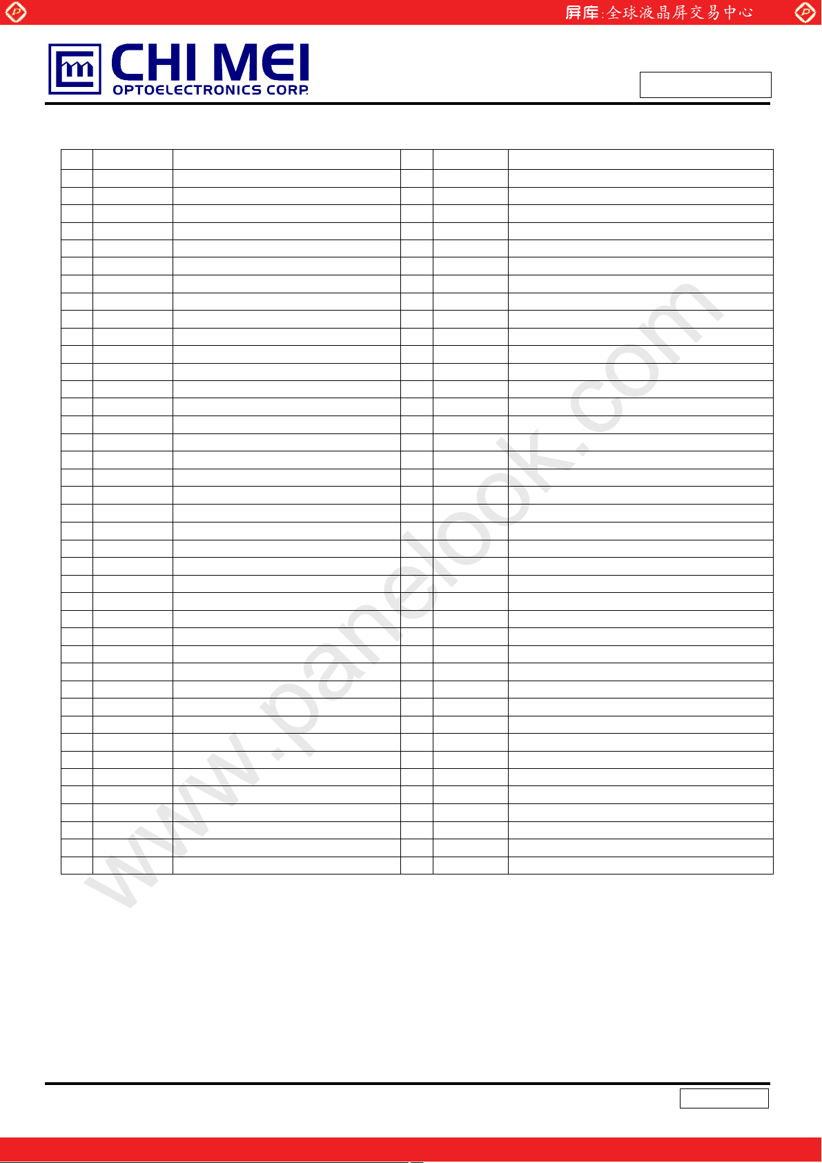
CNX3(XR) Connector Pin Assignment
Pin Symbol Description Pin Symbol Description
1 GND
2 BD1P_12
3 BD1M_12
4 BD0P_12
5 BD0M_12
6 AD1P_12
7 AD1M_12
8 AD0P_12
9 AD0M_12
10 BD1P_11
11 BD1M_11
12 BD0P_11
13 BD0M_11
14 AD1P_11
15 AD1M_11
16 AD0P_11
17 AD0M_11
18 BD1P_11
19 BD1M_11
20 BD0P_10
21 BD0M_10
22 AD1P_10
23 AD1M_10
24 AD0P_10
25 AD1M_10
26 BD1P_9
27 BD1M_9
28 BD0P_9
29 BD0M_9
30 AD1P_9
31 AD1M_9
32 AD0P_9
33 AD0M_9
34 GND
35 D_CLKP
36 D_CLKM
37 BD1P_8
38 BD1M_8
39 BD0P_8
40 BD0M_8
B-Path RSDS data signal
B-Path RSDS data signal
B-Path RSDS data signal
B-Path RSDS data signal
A-Path RSDS data signal
A-Path RSDS data signal
A-Path RSDS data signal
A-Path RSDS data signal
B-Path RSDS data signal
B-Path RSDS data signal
B-Path RSDS data signal
B-Path RSDS data signal
A-Path RSDS data signal
A-Path RSDS data signal
A-Path RSDS data signal
A-Path RSDS data signal
B-Path RSDS data signal
B-Path RSDS data signal
B-Path RSDS data signal
B-Path RSDS data signal
A-Path RSDS data signal
A-Path RSDS data signal
A-Path RSDS data signal
A-Path RSDS data signal
B-Path RSDS data signal
B-Path RSDS data signal
B-Path RSDS data signal
B-Path RSDS data signal
A-Path RSDS data signal
A-Path RSDS data signal
A-Path RSDS data signal
A-Path RSDS data signal
D-Path Data driver clock
D-Path Data driver clock
B-Path RSDS data signal
B-Path RSDS data signal
B-Path RSDS data signal
B-Path RSDS data signal
Ground
Ground
www.panelook.com
Issue Date:Aug.24.2009
Model No.: V420H1-PH5
41 C_CLKP
42 C_CLKM
43 AD1P_8
44 AD1M_8
45 AD0P_8
46 AD0M_8
47 BD1P_7
48 BD1M_7
49 BD0P_7
50 BD0M_7
51 AD1P_7
52 AD1M_7
53 AD0P_7
54 AD0M_7
55 GND
C-Path Data driver clock
C-Path Data driver clock
A-Path RSDS data signal
A-Path RSDS data signal
A-Path RSDS data signal
A-Path RSDS data signal
B-Path RSDS data signal
B-Path RSDS data signal
B-Path RSDS data signal
B-Path RSDS data signal
A-Path RSDS data signal
A-Path RSDS data signal
A-Path RSDS data signal
A-Path RSDS data signal
Ground
Preliminary
13
One step solution for LCD / PDP / OLED panel application: Datasheet, inventory and accessory!
Version 1.0
www.panelook.com
Page 14

Global LCD Panel Exchange Center
CNX4(XR) Connector Pin Assignment
Pin Symbol Description Pin Symbol Description
1 GND
2 VSCM VSCM Power supply 42 NC No connection
3VGH
4 NC No connection 44 NC No connection
5VGL
6 VAA
7 VAA
8 VCM VCM Power supply 48 NC No connection
9 VCM VCM Power supply 49 OE2_R
10 GND
11 G M1
12 GM2
13 GM3
14 GM4
15 GM5
16 GM6
17 GM7
18 GM8
19 GM9
20 GM10
21 GM11
22 GM12
23 GM13
24 GM14
25 GM15
26 GM16
27 GM17
28 GM18
29 GM19
30 GM20
31 GND
32 VCS Charge sharing trace
33 VCS Charge sharing trace
34 VCS Charge sharing trace
35 VCS Charge sharing trace
36 VCS Charge sharing trace
37 VCS Charge sharing trace
38 V33R
39 V33R
40 NC No connection
Gamma Power supply
Gamma Power supply
Gamma Power supply
Gamma Power supply
Gamma Power supply
Gamma Power supply
Gamma Power supply
Gamma Power supply
Gamma Power supply
Gamma Power supply
Gamma Power supply
Gamma Power supply
Gamma Power supply
Gamma Power supply
Gamma Power supply
Gamma Power supply
Gamma Power supply
Gamma Power supply
Gamma Power supply
Gamma Power supply
Ground
Driver Power supply
Driver Power supply
Driver Power supply
Driver Power supply
Ground
Ground
Logic Power supply
Logic Power supply
www.panelook.com
Model No.: V420H1-PH5
41 NC No connection
43 NC No connection
45 NC No connection
46 NC No connection
47 NC No connection
Scan driver output2 enable
50 OE1R
51 STV
52 CKV
53 NC No connection
54 TP1
55 GND
Scan driver output1 enable
Scan driver start pulse
Scan driver clock
RSDS data latch
Ground
Issue Date:Aug.24.2009
Preliminary
14
One step solution for LCD / PDP / OLED panel application: Datasheet, inventory and accessory!
Version 1.0
www.panelook.com
Page 15

Global LCD Panel Exchange Center
5.2 BLOCK DIAGRAM OF INTERFACE
www.panelook.com
Issue Date:Aug.24.2009
Model No.: V420H1-PH5
Preliminary
15
One step solution for LCD / PDP / OLED panel application: Datasheet, inventory and accessory!
Version 1.0
www.panelook.com
Page 16

Global LCD Panel Exchange Center
AR0~AR9: First pixel R data
AG0~AG9: First pixel G data
AB0~AB9: First pixel B data
BR0~BR9: Second pixel R data
BG0~BG9: Second pixel G data
BB0~BB9: Second pixel B data
DE: Data enable signal
DCLK: Data clock signal
Notes (1) The system must have the transmitter to drive the module.
Notes (2) LVDS cable impedance shall be 50 ohms per signal line or about 100 ohms per twist-pair line when it
is used differentially.
www.panelook.com
Issue Date:Aug.24.2009
Model No.: V420H1-PH5
Preliminary
Notes (3) Two pixel data send into the module for every clock cycle. The first pixel of the frame is odd pixel and
the second pixel is even pixel.
16
One step solution for LCD / PDP / OLED panel application: Datasheet, inventory and accessory!
Version 1.0
www.panelook.com
Page 17

Global LCD Panel Exchange Center
5.3 LVDS INTERFACE
VESA Format : SELLVDS = L or Open
JEIDA Format : SELLVDS = H
www.panelook.com
Issue Date:Aug.24.2009
Model No.: V420H1-PH5
Preliminary
AR0~AR9: First Pixel R Data (9; MSB, 0; LSB)
AG0~AG9: First Pixel G Data (9; MSB, 0; LSB)
AB0~AB9: First Pixel B Data (9; MSB, 0; LSB)
DE : Data enable signal
DCLK : Data clock signal
RSVD : Reserved
17
One step solution for LCD / PDP / OLED panel application: Datasheet, inventory and accessory!
Version 1.0
www.panelook.com
Page 18

Global LCD Panel Exchange Center
www.panelook.com
Issue Date:Aug.24.2009
Model No.: V420H1-PH5
Preliminary
5.4 COLOR DATA INPUT ASSIGNMENT
The brightness of each primary color (red, green and blue) is based on the 10-bit gray scale data input for
the color. The higher the binary input, the brighter the color. The table below provides the assignment of the
color versus data input.
0
0
1
0
1
0
1
1
0
0
0
:
:
0
0
0
0
0
0
:
:
1
1
1
0
0
0
:
:
0
0
0
Data Signal
0
0
0
0
1
1
0
0
1
1
0
0
1
1
1
1
0
0
0
0
0
0
:
:
:
:
0
0
0
0
0
0
0
0
0
0
0
0
:
:
:
:
1
1
1
1
1
1
0
0
0
0
0
0
:
:
:
:
0
0
0
0
0
0
0
0
0
0
0
0
0
0
0
0
0
0
0
0
0
0
0
1
1
1
1
0
0
1
1
0
0
1
1
1
1
0
0
0
0
0
0
:
:
:
:
0
0
0
0
0
0
0
0
0
0
0
0
:
:
:
:
1
1
1
1
1
1
0
0
0
0
0
0
:
:
:
:
0
0
0
0
0
0
1
0
0
0
1
1
1
0
0
0
1
1
1
1
1
1
0
0
0
0
0
0
0
0
0
:
:
:
:
:
:
0
0
0
0
0
0
0
0
0
0
0
0
0
0
0
0
0
1
:
:
:
:
:
:
1
1
0
1
1
1
1
1
1
0
0
0
0
0
0
0
0
0
:
:
:
:
:
:
0
0
0
0
0
0
0
0
0
0
1
0
0
0
1
1
1
1
1
0
1
1
1
0
0
1
1
1
0
0
0
0
0
0
0
0
0
:
:
:
:
;
:
0
0
0
0
0
0
0
0
0
0
0
0
1
0
0
0
0
0
:
:
:
:
:
:
1
0
0
0
0
0
1
0
0
0
0
0
0
0
0
0
0
0
:
:
:
:
:
:
0
1
1
0
1
1
0
1
1
0
0
0
0
0
0
0
1
1
1
1
1
1
1
1
1
0
0
0
1
1
1
0
0
0
0
0
0
0
0
0
:
:
:
:
0
0
0
0
0
0
0
0
0
0
0
0
0
0
0
0
0
0
:
:
:
:
0
0
0
0
0
0
0
0
0
0
0
0
0
0
0
0
0
0
:
:
:
:
1
1
1
1
1
1
1
1
1
Basic
Colors
Gray
Scale
Of
Red
Gray
Scale
Of
Green
Gray
Scale
Of
Blue
Color
Black
Red
Green
Blue
Cyan
Magenta
Yel lo w
White
Red (0) / Dark
Red (1)
Red (2)
:
:
Red (1021)
Red (1022)
Red (1023)
Green (0) / Dark
Green (1)
Green (2)
:
:
Green (1021)
Green (1022)
Green (1023)
Blue (0) / Dark
Blue (1)
Blue (2)
:
:
Blue (1021)
Blue (1022)
Blue (1023)
R9 R8 R7 R6 R5 R4 R3 R2 R1 R0 G9 G8 G7 G6 G5 G4 G3 G2 G1 G0 B9 B8 B7 B6 B5 B4 B3 B2 B1 B0
0
0
1
1
0
0
0
0
0
0
1
1
1
1
1
1
0
0
0
0
0
0
1
1
1
1
1
1
0
0
0
0
0
0
:
:
:
:
0
0
0
0
0
0
0
0
0
0
0
0
:
:
:
:
0
0
0
0
0
0
Red Green Blue
0
0
0
0
0
0
0
0
1
1
1
1
1
0
0
0
0
0
0
0
0
0
1
1
1
1
1
1
1
1
1
0
0
0
0
0
0
0
0
0
:
:
:
:
:
:
1
1
1
1
1
1
1
1
1
0
0
0
0
0
0
0
0
0
:
:
:
:
:
:
0
0
0
0
0
0
0
0
0
0
0
0
0
0
0
0
0
0
:
:
:
:
:
:
0
0
0
0
0
0
0
0
0
1
0
0
0
0
0
0
0
0
0
1
1
1
1
1
1
1
1
1
0
0
0
0
0
0
0
0
0
:
:
:
:
:
:
1
1
1
1
1
1
1
1
1
0
0
0
0
0
0
0
0
0
:
:
:
:
:
:
0
0
0
0
0
0
0
0
0
0
0
0
0
0
0
0
0
0
:
:
:
:
:
:
0
0
0
0
0
0
0
0
0
0
1
1
0
0
0
1
0
0
0
0
0
1
1
1
0
1
1
1
1
1
1
0
0
0
0
1
0
1
0
0
:
:
:
:
:
:
0
1
0
1
0
0
1
1
0
0
0
0
0
0
0
0
0
0
:
:
:
:
:
:
0
0
1
0
0
1
0
0
1
0
0
0
0
0
0
0
0
0
:
:
:
:
:
:
0
0
0
0
0
0
0
0
0
Note (1) 0: Low Level Voltage, 1: High Level Voltage
0
0
0
0
0
0
0
0
1
1
1
1
1
1
0
0
1
1
0
0
0
0
0
0
:
:
:
:
:
:
0
0
0
0
0
0
0
0
0
0
0
0
:
:
:
:
:
:
0
0
0
0
0
0
0
0
0
0
0
0
:
:
:
:
:
:
1
1
1
1
1
1
0
0
0
0
0
0
0
1
1
1
1
1
1
1
1
1
0
0
0
1
1
1
0
0
0
0
0
0
0
0
0
:
:
:
:
:
:
0
0
0
0
0
0
0
0
0
0
0
0
0
0
0
0
0
0
:
:
:
:
:
:
0
0
0
0
0
0
0
0
0
0
0
0
0
0
1
0
1
0
:
:
:
:
:
:
1
0
1
1
1
0
1
1
1
18
One step solution for LCD / PDP / OLED panel application: Datasheet, inventory and accessory!
Version 1.0
www.panelook.com
Page 19

Global LCD Panel Exchange Center
6. INTERFACE TIMING
6.1 INPUT SIGNAL TIMING SPECIFICATIONS
(Ta = 25 ± 2 ºC)
The input signal timing specifications are shown as the following table and timing diagram.
Signal Item Symbol Min. Typ. Max. Unit Note
www.panelook.com
Issue Date:Aug.24.2009
Model No.: V420H1-PH5
Preliminary
LVDS Receiver
Clock
LVDS Receiver
Data
Vertical
Active Display
Term
Horizontal
Active Display
Term
Note : Since the module is operated in DE only mode, Hsync and Vsync input signals should be set to low logic
level. Otherwise, this module would operate abnormally.
Frequency 1/Tc 60 74.25 78 MHz -
Input cycle to
cycle jitter
Setup Time Tlvsu 600 - - ps -
Hold Time Tlvhd 600 - - ps -
Frame Rate - 120 - Hz
Total Tv 1115 1125 1135 Th
Display Tvd 1080 1080 1080 Th -
Blank Tvb 35 45 55 Th -
Tota l Th 525 550 575 Tc
Display Thd 480 480 480 Tc -
Blank Thb 45 70 95 Tc -
Trcl - - 200 ps -
Tv=Tvd+T vb
Th=Thd+Thb
Valid display data (480 clocks)
19
One step solution for LCD / PDP / OLED panel application: Datasheet, inventory and accessory!
Version 1.0
www.panelook.com
Page 20

Global LCD Panel Exchange Center
LVDS INPUT INTERFACE TIMING DIAGRAM
RXCLK +
RXn +/-
Tlvsu Tlvhd
www.panelook.com
Issue Date:Aug.24.2009
Model No.: V420H1-PH5
Preliminary
Tc
1T
14
3T
14
5T
14
7T
14
9T
14
11T
14
13T
14
20
One step solution for LCD / PDP / OLED panel application: Datasheet, inventory and accessory!
Version 1.0
www.panelook.com
Page 21

Global LCD Panel Exchange Center
6.2 POWER ON/OFF SEQUENCE
(Ta = 25 ± 2 ºC)
To prevent a latch-up or DC operation of LCD module, the power on/off sequence should follow the diagram
below.
0.5
ЉЉЉЉ
T
1
ЉЉЉЉ
0
ЉЉЉЉ
T
2
ЉЉЉЉ
0
ЉЉЉЉ
T
3
ЉЉЉЉ
500ms
100ms
10ms
100ms
ЉЉЉЉ
T4
0V
LVDS Signals
0V
0
ЉЉЉЉ
T
7
ЉЉЉЉ
0
ЉЉЉЉ
T2
T
8
ЉЉЉЉ
T3
www.panelook.com
T
2
Power On
T7
VALI D
3
T1
T
Issue Date:Aug.24.2009
Model No.: V420H1-PH5
Preliminary
0.1V
cc
T4
Power Off
8
T
Option Signals
(SELLVDS…)
Backlight (Recommended)
ЉЉЉЉ
500ms
T5
50%
50%
5
T
6
T
Power ON/OFF Sequence
Note.
(1) The supply voltage of the external system for the module input should follow the definition of Vcc.
(2) Apply the lamp voltage within the LCD operation range. When the backlight turns on before the LCD
operation or the LCD turns off before the backlight turns off, the display may momentarily become abnormal
screen.
(3) In case of VCC is in off level, please keep the level of input signals on the low or high impedance. If T2<0,
that maybe cause electrical overstress failures.
(4) T4 should be measured after the module has been fully discharged between power off and on period.
(5) Interface signal shall not be kept at high impedance when the power is on.
21
One step solution for LCD / PDP / OLED panel application: Datasheet, inventory and accessory!
Version 1.0
www.panelook.com
Page 22

Global LCD Panel Exchange Center
7. OPTICAL CHARACTERISTICS
7.1 TEST CONDITIONS
Item Symbol Value Unit
www.panelook.com
Issue Date:Aug.24.2009
Model No.: V420H1-PH5
Preliminary
Ambient Temperature Ta
Ambient Humidity Ha
Supply Voltage VCC 12 V
Input Signal According to typical value in "3. ELECTRICAL CHARACTERISTICS"
Lamp Current IL 8.7/10.2 mA
Oscillating Frequency (Inverter) FW
Vertical Frame Rate Fr 120 Hz
The LCD module should be stabilized at given temperature for 1 hour to avoid abrupt temperature change during
measuring. In order to stabilize the luminance, the measurement (CS-1000 or CA-210 calibrated by CS-1000)
should be executed after lighting backlight for 1 hour in a windless room.
LCD Module
LCD Panel
25±2
50±10
42±3
oC
%RH
KHz
Center of the Screen
Display Color Analyzer
(Minolta CA210)
Light Shield Room
(Ambient Luminance < 2 lux)
22
One step solution for LCD / PDP / OLED panel application: Datasheet, inventory and accessory!
Version 1.0
www.panelook.com
Page 23

Global LCD Panel Exchange Center
7.2 OPTICAL SPECIFICATIONS
The relative measurement methods of optical characteristics are shown in 7.2. The following items should be
measured under the test conditions described in 7.1 and stable environment shown in 7.1.
Item Symbol Condition Min. Typ. Max. Unit Note
Contrast Ratio CR 3000 4000 - - Note (2)
www.panelook.com
Issue Date:Aug.24.2009
Model No.: V420H1-PH5
Preliminary
Response Time
Noraml mode LC 400 500 - cd/m2Note (4)Center
Luminance of
White
White Variation
Cross Talk CT - - 4 % Note (5)
Color
Chromaticity
ECO mode LC 350 450 - cd/m
Red
Green
Blue
White
Gray to
gray
δW
Rx 0.649 -
Ry 0.334 -
Gx 0.267 -
Gy 0.610 -
Bx 0.149 -
By 0.060 -
Wx 0.280 -
Wy
θx=0°, θy =0°
Viewing angle
at normal direction
- 4.0 8.0 ms Note (3)
Note (4),
2
- - 1.3 - Note (6)
Typ.
-0.03
0.285
Typ.
+0.03
-
(7)
-
Color Gamut C.G
θx+
Horizontal
θx-
Viewing Angle
θY+
Vertical
θY-
Note (1) Definition of Viewing Angle (θx, θy):
Viewing angles are measured by Eldim EZ-Contrast 160R
CR≥20
23
- 72 - % NTSC
80 88 -
80 88 -
Deg. Note (1)
80 88 -
80 88 -
One step solution for LCD / PDP / OLED panel application: Datasheet, inventory and accessory!
Version 1.0
www.panelook.com
Page 24

Global LCD Panel Exchange Center
www.panelook.com
Issue Date:Aug.24.2009
Model No.: V420H1-PH5
Preliminary
Note (2) Definition of Contrast Ratio (CR):
The contrast ratio can be calculated by the following expression.
Contrast Ratio (CR) =
CR = CR (5), where CR (X) is corresponding to the Contrast Ratio of the point X at the figure in Note (6).
Note (3) Definition of Gray-to-Gray Switching Time:
pixels whiteall withLuminance Surface
pixels black all withLuminance Surface
The driving signal means the signal of gray level 0, 124, 252, 380, 508, 636, 764, 892 and 1023.
Gray to gray average time means the average switching time of gray level 0, 124, 252, 380, 508, 636,
764, 892, 1023 to each other.
, L
Note (4) Definition of Luminance of White (L
Measure the luminance of gray level 1023 at center point and 5 points
= L (5), where L (X) is corresponding to the luminance of the point X at the figure in Note (6).
L
C
):
C
AVE
24
One step solution for LCD / PDP / OLED panel application: Datasheet, inventory and accessory!
Version 1.0
www.panelook.com
Page 25

Global LCD Panel Exchange Center
Note (5) Definition of Cross Talk (CT):
www.panelook.com
Issue Date:Aug.24.2009
Model No.: V420H1-PH5
Preliminary
CT = | YB – YA | / YA
Where:
YA = Luminance of measured location without gray level 0 pattern (cd/m2)
YB = Luminance of measured location with gray level 0 pattern (cd/m2)
Note (6) Definition of White Variation (
Measure the luminance of gray level 1023 at 5 points
×
100 (%)
δ
W):
δ
W = Maximum [L (1), L (2), L (3), L (4), L (5)] / Minimum [L (1), L (2), L (3), L (4), L (5)]
W
W
3W
Note (7) ECO mode:
Horizontal Line
D
D
4
D
2
1 2
4
5
3D
4
X
Test point :
X = 1 ~ 5
2
3 4
4
ECO mode was selected by inverter pin: A_DIM.
25
Version 1.0
One step solution for LCD / PDP / OLED panel application: Datasheet, inventory and accessory!
www.panelook.com
Page 26

Global LCD Panel Exchange Center
www.panelook.com
Issue Date:Aug.24.2009
Model No.: V420H1-PH5
Preliminary
8. PRECAUTIONS
8.1 ASSEMBLY AND HANDLING PRECAUTIONS
[ 1 ] Do not apply rough force such as bending or twisting to the module during assembly.
[ 2 ] It is recommended to assemble or to install a module into the user’s system in clean working areas. The
dust and oil may cause electrical short or worsen the polarizer.
[ 3 ] Do not apply pressure or impulse to the module to prevent the damage of LCD panel and Backlight.
[ 4 ] Always follow the correct power-on sequence when the LCD module is turned on. This can prevent the
damage and latch-up of the CMOS LSI chips.
[ 5 ] Do not plug in or pull out the I/F connector while the module is in operation.
[ 6 ] Do not disassemble the module.
[ 7 ] Use a soft dry cloth without chemicals for cleaning, because the surface of polarizer is very soft and easily
scratched.
[ 8 ] Moisture can easily penetrate into LCD module and may cause the damage during operation.
[ 9 ] When storing modules as spares for a long time, the following precaution is necessary.
[ 9.1 ] Do not leave the module in high temperature, and high humidity for a long time. It is highly
к
recommended to store the module with temperature from 0 to 35
condensation.
[ 9.2 ] The module shall be stored in dark place. Do not store the TFT-LCD module in direct sunlight or
fluorescent light.
[ 10 ] When ambient temperature is lower than 10ºC, the display quality might be reduced. For example, the
response time will become slow, and the starting voltage of CCFL will be higher than that of room
temperature.
at normal humidity without
8.2 SAFETY PRECAUTIONS
[ 1 ] The startup voltage of a Backlight is approximately 1000 Volts. It may cause an electrical shock while
assembling with the inverter. Do not disassemble the module or insert anything into the Backlight unit.
[ 2 ] If the liquid crystal material leaks from the panel, it should be kept away from the eyes or mouth. In case of
contact with hands, skin or clothes, it has to be washed away thoroughly with soap.
[ 3 ] After the module’s end of life, it is not harmful in case of normal operation and storage.
26
Version 1.0
One step solution for LCD / PDP / OLED panel application: Datasheet, inventory and accessory!
www.panelook.com
Page 27

Global LCD Panel Exchange Center
9. DEFINITION OF LABELS
9.1 OPEN CELL LABEL
The barcode nameplate is pasted on each open cell as illustration for CMO internal control.
9.2 CARTON LABEL
www.panelook.com
Issue Date:Aug.24.2009
Model No.: V420H1-PH5
Preliminary
V420H1-PH5
The barcode nameplate is pasted on each box as illustration, and its definitions are as following explanation.
(a) Model Name: V420H1-PH5
(b) Carton ID: CMO internal control
(c) Quantities: 9 pcs
27
Version 1.0
One step solution for LCD / PDP / OLED panel application: Datasheet, inventory and accessory!
www.panelook.com
Page 28

Global LCD Panel Exchange Center
10. PACKAGING
10.1 PACKAGING SPECIFICATIONS
(1) 9PCS LCD TV Panels / 1 Box
(2) Box dimensions : 1225 (L) X 801 (W) X 234 (H)
(3) Weight : approximately 32.2 Kg
10.2 PACKING METHOD
Figures 10-1 and 10-2 are the packing method
www.panelook.com
Issue Date:Aug.24.2009
Model No.: V420H1-PH5
Preliminary
Figure.10-1 packing method
28
Version 1.0
One step solution for LCD / PDP / OLED panel application: Datasheet, inventory and accessory!
www.panelook.com
Page 29

Global LCD Panel Exchange Center
www.panelook.com
Issue Date:Aug.24.2009
Model No.: V420H1-PH5
Preliminary
Figure.10-2 packing method
29
Version 1.0
One step solution for LCD / PDP / OLED panel application: Datasheet, inventory and accessory!
www.panelook.com
Page 30

Global LCD Panel Exchange Center
11. MECHANICAL CHARACTERISTICS
www.panelook.com
Issue Date:Aug.24.2009
Model No.: V420H1-PH5
Preliminary
ڻႝηިҽԖϦљ
CHI MEI
30
Version 1.0
One step solution for LCD / PDP / OLED panel application: Datasheet, inventory and accessory!
www.panelook.com
Page 31

Global LCD Panel Exchange Center
www.panelook.com
Issue Date:Aug.24.2009
Model No.: V420H1-PH5
Preliminary
ڻႝηިҽԖϦљ
CHI MEI
31
Version 1.0
One step solution for LCD / PDP / OLED panel application: Datasheet, inventory and accessory!
www.panelook.com
Page 32

Global LCD Panel Exchange Center
www.panelook.com
Issue Date:Aug.24.2009
Model No.: V420H1-PH5
Preliminary
ڻႝηިҽԖϦљ
CHI MEI
32
Version 1.0
One step solution for LCD / PDP / OLED panel application: Datasheet, inventory and accessory!
www.panelook.com
Page 33

Global LCD Panel Exchange Center
www.panelook.com
Appendix – TWO Wire BUS INTRODUCTION
A.1 PIN ASSIGNMENT
51pins LVDS connector
Pin8: SCL
Pin9: SDA
A.2 I2C BUS APPLICATION NOTE
I2C bus: (The I2C bus must for MEMC only or prevent the I2C bus voltage drop down in initial state)
Issue Date:Aug.24.2009
Model No.: V420H1-PH5
Preliminary
A.3 TWO WIRE BUS DEVICE ADDRESS
Two wire device address: default is 0x40, 1 byte
Two wire command: the range is 0x00 to 0xFF, 1 byte, see the two wire command table.
Two wire bus format:
33
Version 1.0
One step solution for LCD / PDP / OLED panel application: Datasheet, inventory and accessory!
www.panelook.com
Page 34

Global LCD Panel Exchange Center
A.4 TWO WAY TO CONTROL THE TWO WIRE BUS
There are two options to control the two wires bus command.
Two wire bus 6 bytes format
www.panelook.com
Issue Date:Aug.24.2009
Model No.: V420H1-PH5
Preliminary
Two wire bus 3 bytes format
Note:
A transmission basically consists of a START condition, a SLA+R/W, one or more data packets and a STOP
condition. An empty message, consisting of a START followed by a STOP condition, is illegal. Note that the
wired-ANDing of the SCL line can be used to implement handshaking between the master and the slave. The slave
can extend the SCL low period by pulling the SCL line low. This is useful if the clock speed set up by the master is too
fast for the slave, or the slave needs extra time for processing between the data transmissions. The slave extending
the SCL low period will not affect the SCL high period, which is determined by the master. As a consequence, the
slave can reduce the TWI data transfer speed by prolonging the SCL duty cycle.
34
Version 1.0
One step solution for LCD / PDP / OLED panel application: Datasheet, inventory and accessory!
www.panelook.com
Page 35

Global LCD Panel Exchange Center
A.5 TWO WIRE BUS COMMAND TABLE
There is two wire bus command table.
Command Name
All OSD Protection 0x00 R/W OSDx Enable Flag Contorl
OSD1_Start_Protection 0x01 R/W OSD1 Protection Start Position
OSD2_Start_Protection 0x02 R/W OSD2 Protection Start Position
OSD3_Start_Protection 0x03 R/W OSD3 Protection Start Position
OSD4_Start_Protection 0x04 R/W OSD4 Protection Start Position
OSD1_End_Protection 0x05 R/W OSD1 Protection End Position
OSD2_End_Protection 0x06 R/W OSD2 Protection End Position
OSD3_End_Protection 0x07 R/W OSD3 Protection End Position
OSD4_End_Protection 0x08 R/W OSD4 Protection End Position
Demo Window 0x09 R/W ME Performance Demo
MEMC Level 0x0A R/W ME Performance
GV Mode 0x0B R/W ME Operation
Blanking 0x0C R/W Blinking the screen
www.panelook.com
Access
Mode
Description
Issue Date:Aug.24.2009
Model No.: V420H1-PH5
Preliminary
35
Version 1.0
One step solution for LCD / PDP / OLED panel application: Datasheet, inventory and accessory!
www.panelook.com
Page 36

Global LCD Panel Exchange Center
Enable All OSD Protection
www.panelook.com
Issue Date:Aug.24.2009
Model No.: V420H1-PH5
Preliminary
OSD # 1~4 Start Protection
OSD # 1~4 End Protection
36
Version 1.0
One step solution for LCD / PDP / OLED panel application: Datasheet, inventory and accessory!
www.panelook.com
Page 37

Global LCD Panel Exchange Center
Demo Window
www.panelook.com
Issue Date:Aug.24.2009
Model No.: V420H1-PH5
Preliminary
MEMC Level
GV Mode
37
Version 1.0
One step solution for LCD / PDP / OLED panel application: Datasheet, inventory and accessory!
www.panelook.com
Page 38

Global LCD Panel Exchange Center
Blanking (Enable/Disable)
www.panelook.com
Issue Date:Aug.24.2009
Model No.: V420H1-PH5
Preliminary
38
Version 1.0
One step solution for LCD / PDP / OLED panel application: Datasheet, inventory and accessory!
www.panelook.com
Page 39

Global LCD Panel Exchange Center
A.6 TWO WIRE BUS REQUIREMENT
www.panelook.com
Issue Date:Aug.24.2009
Model No.: V420H1-PH5
Preliminary
39
Version 1.0
One step solution for LCD / PDP / OLED panel application: Datasheet, inventory and accessory!
www.panelook.com
Page 40

Global LCD Panel Exchange Center
A.7 THE TWO WIRE BUS SEQUENCE
Two Wire command can be initialized during 20ms to 60ms.
www.panelook.com
Issue Date:Aug.24.2009
Model No.: V420H1-PH5
Preliminary
Exam ple:
The previous state is strong mode, and the power is reset. The two wire command (strong mode command)
must be initialized during 20ms to 60ms.
40
Version 1.0
One step solution for LCD / PDP / OLED panel application: Datasheet, inventory and accessory!
www.panelook.com
 Loading...