

Page 1
Global LCD Panel Exchange Center
TFT LCD Approval Specification
MODEL NO.: V420H1 – LH3
Customer: _________________________________
www.panelook.com
Issue Date:Dec.28.2007
Model No.: V420H1-LH3
Preliminary
Approved by:_______________________________
Note:
TV Head Division
Approved By
LY Chen
QRA Dept. Product Development Div.
Reviewed By
Tomy Chen WT Lin
LCD TV Marketing and Product Management Div.
Prepared By
Ken Wu CY Chang
1
One step solution for LCD / PDP / OLED panel application: Datasheet, inventory and accessory!
Version 1.0
www.panelook.com
Page 2
Global LCD Panel Exchange Center
www.panelook.com
Issue Date:Dec.28.2007
Model No.: V420H1-LH3
Preliminary
CONTENTS
REVISION HISTORY.........................................................................................................................................................4
1. GENERAL DESCRIPTION............................................................................................................................................ 5
1.1 OVERVIEW ..........................................................................................................................................................5
1.2 FEATURES...........................................................................................................................................................5
1.3 APPLICATION ......................................................................................................................................................5
1.4 GENERAL SPECIFICATIONS .............................................................................................................................5
1.5 MECHANICAL SPECIFICATIONS ....................................................................................................................... 6
2. ABSOLUTE MAXIMUM RATINGS ................................................................................................................................7
2.1 ELECTRICAL ABSOLUTE RATINGS ..................................................................................................................7
2.1.1 TFT LCD MODULE ....................................................................................................................................7
2.2 ABSOLUTE RATINGS OF ENVIRONMENT........................................................................................................7
2.3 RELIABILITY TEST CONDITION.........................................................................................................................8
3. ELECTRICAL CHARACTERISTICS .............................................................................................................................9
3.1 TFT LCD MODULE ..............................................................................................................................................9
3.2 BACKLIGHT CONNECTOR PIN CONFIGURATION......................................................................................... 11
3.2.1 LAMP SPECIFICATION...........................................................................................................................11
3.2.2 ELECTRICAL SPECIFICATION............................................................................................................... 11
4. BLOCK DIAGRAM OF INTERFACE ...........................................................................................................................12
4.1 TFT LCD MODULE ............................................................................................................................................12
5. INPUT TERMINAL PIN ASSIGNMENT.......................................................................................................................13
5.1 TFT LCD Module Input.......................................................................................................................................13
5.2 BACKLIGHT UNIT..............................................................................................................................................17
5.3 BLOCK DIAGRAM OF INTERFACE.................................................................................................................. 18
5.4 LVDS INTERFACE.............................................................................................................................................20
5.5 COLOR DATA INPUT ASSIGNMENT ................................................................................................................21
6. INTERFACE TIMING...................................................................................................................................................22
6.1 INPUT SIGNAL TIMING SPECIFICATIONS ......................................................................................................22
6.2 POWER ON/OFF SEQUENCE.......................................................................................................................... 24
7. OPTICAL CHARACTERISTICS ..................................................................................................................................25
2
Version 1.0
One step solution for LCD / PDP / OLED panel application: Datasheet, inventory and accessory!
www.panelook.com
Page 3

Global LCD Panel Exchange Center
www.panelook.com
Issue Date:Dec.28.2007
Model No.: V420H1-LH3
Preliminary
7.1 TEST CONDITIONS...........................................................................................................................................25
7.2 OPTICAL SPECIFICATIONS .............................................................................................................................26
8. PRECAUTIONS...........................................................................................................................................................29
8.1 ASSEMBLY AND HANDLING PRECAUTIONS .................................................................................................29
8.2 SAFETY PRECAUTIONS ..................................................................................................................................29
9. DEFINITION OF LABELS............................................................................................................................................30
9.1 CMO MODULE LABEL ......................................................................................................................................30
10. PACKAGING..............................................................................................................................................................31
10.1 PACKAGING SPECIFICATIONS .....................................................................................................................31
10.2 PACKAGING METHOD....................................................................................................................................31
11. MECHANICAL CHARACTERISTICS ........................................................................................................................33
3
One step solution for LCD / PDP / OLED panel application: Datasheet, inventory and accessory!
Version 1.0
www.panelook.com
Page 4
Global LCD Panel Exchange Center
REVISION HISTORY
Version Date
Ver.1.0
Dec, 28,’07
Page
(New)
All All Preliminary Specification was first issued.
www.panelook.com
Issue Date:Dec.28.2007
Model No.: V420H1-LH3
Preliminary
Section Description
4
One step solution for LCD / PDP / OLED panel application: Datasheet, inventory and accessory!
Version 1.0
www.panelook.com
Page 5
Global LCD Panel Exchange Center
1. GENERAL DESCRIPTION
1.1 OVERVIEW
V420H1-LH3 is a 42” TFT Liquid Crystal Display module with 18-CCFL Backlight unit and 4ch-LVDS interface.
This module supports 1920 x 1080 Full HDTV format and can display true 1.07G colors (10-bit/color). The
inverter module for backlight isn’t built-in.
1.2 FEATURES
Ё High brightness (500 nits)
Ё High contrast ratio (1800:1)
Ё Fast response time (Gray to gray average 4.0 ms)
Ё High color saturation (NTSC 72%)
Ё Full HDTV (1920 x 1080 pixels) resolution, true HDTV format
Ё DE (Data Enable) only mode
www.panelook.com
Issue Date:Dec.28.2007
Model No.: V420H1-LH3
Preliminary
Ё LVDS (Low Voltage Differential Signaling) interface
Ё Optimized response time for 100 Hz frame rate
Ё Ultra wide viewing angle : Super MVA technology
Ё RoHS compliance
1.3 APPLICATION
Ё Standard Living Room TVs.
Ё Public Display Application.
Ё Home Theater Application.
Ё MFM Application.
1.4 GENERAL SPECIFICATIONS
Item Specification Unit Note
Active Area 930.24(H) x 523.26 (V) (42.02” diagonal) mm
Bezel Opening Area 939 (H) x 531 (V) mm
Driver Element a-si TFT active matrix - -
Pixel Number 1920 x R.G.B. x 1080 pixel -
Pixel Pitch(Sub Pixel) 0.1615 (H) x 0.4845 (V) mm -
Pixel Arrangement RGB vertical stripe - -
(1)
Display Colors 1.07G color -
Display Operation Mode Transmissive mode / Normally black - -
Surface Treatment Anti-Glare coating / 3H - (2)
Note (1) Please refer to the attached drawings in chapter 9 for more information about the front and back outlines.
Note (2) The spec. of the surface treatment is temporarily for this phase. CMO reserves the rights to change this
feature.
5
One step solution for LCD / PDP / OLED panel application: Datasheet, inventory and accessory!
Version 1.0
www.panelook.com
Page 6
Global LCD Panel Exchange Center
1.5 MECHANICAL SPECIFICATIONS
Item Min. Typ. Max. Unit Note
Horizontal (H) 982.0 983.0 984.0 mm
www.panelook.com
Issue Date:Dec.28.2007
Model No.: V420H1-LH3
Preliminary
Module Size
Weight 11500 12000 12500 g -
Note (1) Please refer to the attached drawings for more information of front and back outline dimensions.
Note (2) Module Depth is between bezel to T-CON cover.
Vertical (V) 575.0 576.0 577.0 mm
Depth (D) 46.3 47.3 48.3 mm
(1), (2)
6
One step solution for LCD / PDP / OLED panel application: Datasheet, inventory and accessory!
Version 1.0
www.panelook.com
Page 7
Global LCD Panel Exchange Center
2. ABSOLUTE MAXIMUM RATINGS
2.1 ELECTRICAL ABSOLUTE RATINGS
2.1.1 TFT LCD MODULE
www.panelook.com
Issue Date:Dec.28.2007
Model No.: V420H1-LH3
Preliminary
Item Symbol
Min. Max.
Power Supply Voltage VCC -0.3 14.0 V
Logic Input Voltage VIN -0.3 3.6 V
Value
Unit Note
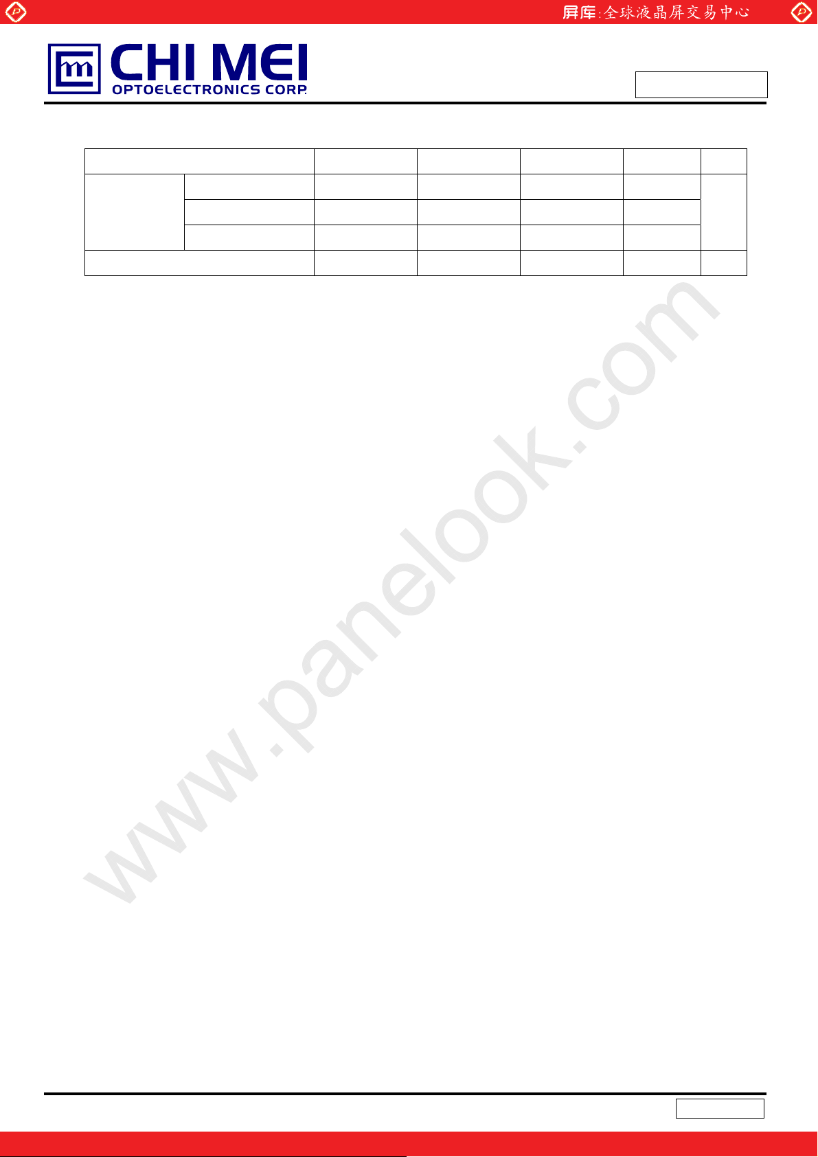
2.2 ABSOLUTE RATINGS OF ENVIRONMENT
Item Symbol
Min. Max.
Storage Temperature TST -20 +60 ºC (1)
Operating Ambient Temperature TOP 0 50 ºC (1), (2)
Shock (Non-Operating) SNOP - 50 G (3), (5)
Vibration (Non-Operating) VNOP - 1.0 G (4), (5)
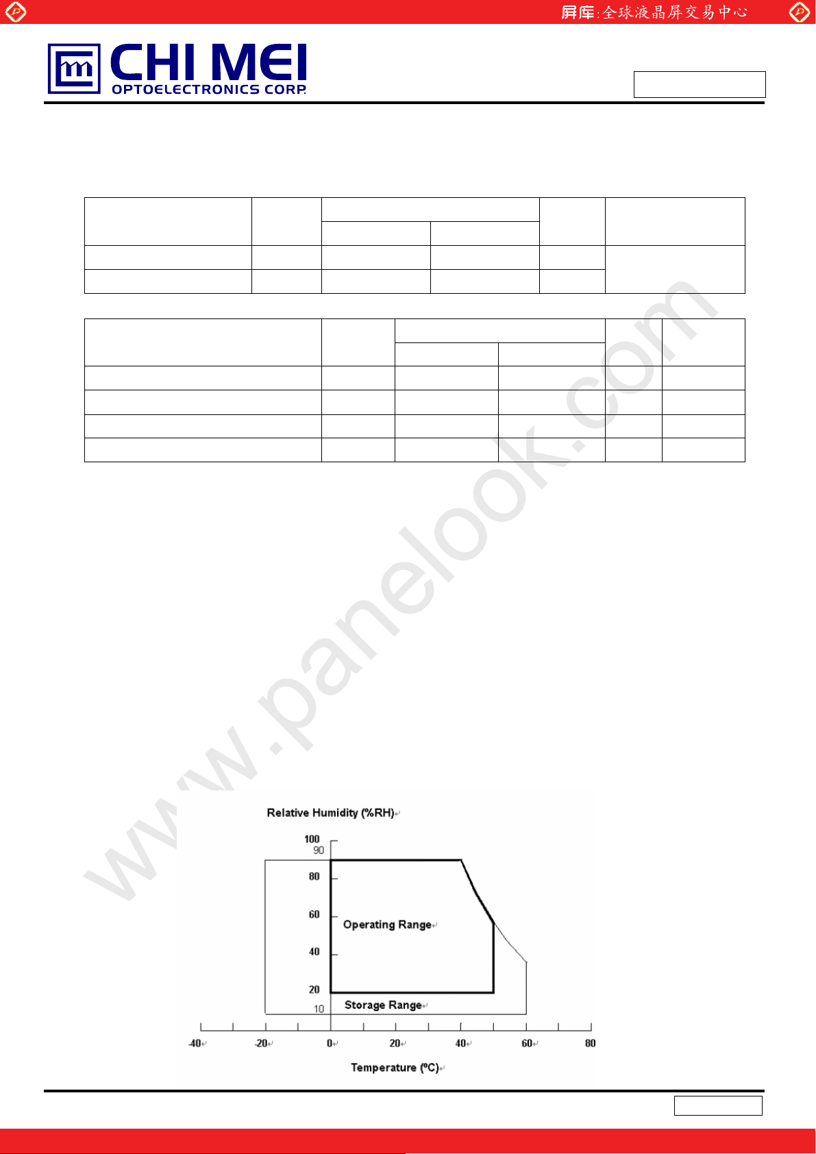
Note (1) Temperature and relative humidity range is shown in the figure below.
(a) 90 %RH Max. (Ta Љ 40 ºC).
(b) Wet-bulb temperature should be 39 ºC Max. (Ta > 40 ºC).
(c) No condensation.
Note (2) The maximum operating temperature is based on the test condition that the surface temperature of
display area is less than or equal to 65 ºC with LCD module alone in a temperature controlled chamber.
Value
Unit Note
(1)
Thermal management should be considered in final product design to prevent the surface temperature of
display area from being over 65 ºC. The range of operating temperature may degrade in case of
improper thermal management in final product design.
Note (3) 11 ms, half sine wave, 1 time for ± X, ± Y, ± Z.
Note (4) 10 ~ 200 Hz, 10 min, 1 time each X, Y, Z.
Note (5) At testing Vibration and Shock, the fixture in holding the module has to be hard and rigid enough so that
the module would not be twisted or bent by the fixture.
7
One step solution for LCD / PDP / OLED panel application: Datasheet, inventory and accessory!
Version 1.0
www.panelook.com
Page 8
Global LCD Panel Exchange Center
2.3 RELIABILITY TEST CONDITION
No Test Item Codition
www.panelook.com
Issue Date:Dec.28.2007
Model No.: V420H1-LH3
Preliminary
1 High temperature storage test
2 Low temperature storage test
High temperature high humidity storage
3
test
4 High temperature operation test
5 Low temperature operation test
High temperature high humidity operation
6
test
7 Vibration test (non-operation)
8 Shock test (non-operation)
Ta = 60к, 240hrs
Ta = -20к, 240hrs
Ta = 50к, 90%RH, 240hrs
Ta = 50к, 240hrs
Ta = 0к, 240hrs
Ta = 50к, 80%RH, 240hrs
Wave form: Sine wave
Vibration level: 1.0G
Fre. range : 10~200Hz
Duration: X, Y, Z, 10min,
One time each direction
Wave form: half sine wave
Shock level: 50G
X, Y, Z, 11ms
One time each direction
8
One step solution for LCD / PDP / OLED panel application: Datasheet, inventory and accessory!
Version 1.0
www.panelook.com
Page 9
Global LCD Panel Exchange Center
3. ELECTRICAL CHARACTERISTICS
3.1 TFT LCD MODULE
(Ta = 25 ± 2 ºC)
Parameter Symbol
Power Supply Voltage VCC 10.8 12 13.2 V (1)
Power Supply Ripple Voltage VRP - - 350 mV
Rush Current IRUSH - - 6.5 A (2)
White Pattern - - 2.2 2.8 A
www.panelook.com
Issue Date:Dec.28.2007
Model No.: V420H1-LH3
Preliminary
Value
Unit Note
Min. Typ. Max.
Power Supply Current
Differential Input High Threshold
Voltage
Differential Input Low Threshold
LVDS
Interface
CMOS
interface
Note (1) The module should be always operated within the above ranges.
Note (2) Measurement condition:
Voltage
Common Input Voltage VLVC 1.125 1.25 1.375 V
Terminating Resistor RT - 100 - ohm
Input High Threshold Voltage VIH 2.7 - 3.3 V
Input Low Threshold Voltage VIL 0 - 0.7 V
Mosaic Pattern
Black Pattern - - 1.5 - A
-
VLVTH - - 100 mV
VLVTL -100 - - mV
- 1.8 - A
(3)
9
One step solution for LCD / PDP / OLED panel application: Datasheet, inventory and accessory!
Version 1.0
www.panelook.com
Page 10
Global LCD Panel Exchange Center
www.panelook.com
Issue Date:Dec.28.2007
Model No.: V420H1-LH3
Preliminary
Note (3) The specified power supply current is under the conditions at Vcc = 12 V, Ta = 25 ± 2 ºC, fv = 100 Hz,
whereas a power dissipation check pattern below is displayed.
a. White Pattern
c. Black Pattern
b. Mosaic Pattern
Active AreaActive Area
R
R
Active Area
10
One step solution for LCD / PDP / OLED panel application: Datasheet, inventory and accessory!
Version 1.0
www.panelook.com
Page 11
Global LCD Panel Exchange Center
www.panelook.com
3.2 BACKLIGHT CONNECTOR PIN CONFIGURATION
3.2.1 LAMP SPECIFICATION
(Ta = 25 ± 2 ºC)
Issue Date:Dec.28.2007
Model No.: V420H1-LH3
Preliminary
Parameter Symbol
Value
Min. Typ. Max.
- - 2370 VRMS Ta = 0 ºC
Lamp Starting Voltage VSL
- - 2160 VRMS Ta = 25 ºC
Lamp Voltage VL 1368 1520 1672 VRMS
Lamp Current IL 5.5 6.0 6.5 mARMS
Lamp Frequency FL 40 - 80 KHz
Lamp Life Time LBL 50,000 60,000 - Hrs (1)
Note(1) Condition: PWM 100% dimming duty ratio
3.2.2 ELECTRICAL SPECIFICATION
(Ta = 25 ± 2 ºC)
Value
Parameter Symbol
Min. Typ. Max.
- 2185 2403 VRMS (1), Ta = 0 ºC
BL Starting Voltage VSBL
- 2080 2288 VRMS (1), Ta = 25 ºC
Unit Note
Unit Note
BL Lamp Voltage VBL 1684 1760 1836 VRMS (1)
BL Lamp Current IBL 105 115 125 mARMS 18 lamps
Oscillating Frequency FW 43 45 47 KHz
PWM Dimming Range PDIM 20 - 100 % (2)
Striking Time ST - - 2 Sec
Lamp Type - Straight Type -
Number of Lamps - 18 PCS
Type of Current Balance - C-Balance -
C Ballaster CB - 22 - pF
Note (1) Single size: Half lamp voltage + capacitor voltage
Note (2) V420H1-LH3 are designed without Inverter. These items are for reference and based on V420H1-L07
Inverter model.
11
One step solution for LCD / PDP / OLED panel application: Datasheet, inventory and accessory!
Version 1.0
www.panelook.com
Page 12

Global LCD Panel Exchange Center
4. BLOCK DIAGRAM OF INTERFACE
4.1 TFT LCD MODULE
www.panelook.com
Issue Date:Dec.28.2007
Model No.: V420H1-LH3
Preliminary
DRX0(+/-)
DRX1(+/-)
DRX2(+/-)
DRX3(+/-)
DRX4(+/-)
DCLK(+/-)
CRX0(+/-)
CRX1(+/-)
CRX2(+/-)
CRX3(+/-)
CRX4(+/-)
CCLK(+/-)
BRX0(+/-)
BRX1(+/-)
BRX2(+/-)
BRX3(+/-)
BRX4(+/-)
BCLK(+/-)
ARX0(+/-)
ARX1(+/-)
ARX2(+/-)
ARX3(+/-)
ARX4(+/-)
ACLK(+/-)
SELLVDS
ODSEL
Vcc
GND
FRAME
BUFFER
TIMING
CONTROLLER
(SLAVE)
FRAME
BUFFER
TIMING
CONTROLLER
(MASTER)
TFT LCD PANEL
1920 X 3 X 1080
DATA DRIVER(RSDS)
CN1
H.V.
H.V.
N.C.
INVERTER
CONNECTOR
CN1: 65002WR-03
DC/DC CONVERTER &
REFERENCE
VOLTAGE
GENERATOR
BACKLIGHT
UNIT
INVERTER
CONNECTOR
CN2: 65002WR-03
CN2
H.V.
H.V.
N.C.
12
One step solution for LCD / PDP / OLED panel application: Datasheet, inventory and accessory!
Version 1.0
www.panelook.com
Page 13

Global LCD Panel Exchange Center
5. INPUT TERMINAL PIN ASSIGNMENT
5.1 TFT LCD Module Input
CNF1 Connector Pin Assignment (FI-RE51S-HF(JAE) or equivalent)
Pin Name Description Note
1 GND Ground
2 N.C. No Connection (1)
3 N.C. No Connection (1)
4 N.C. No Connection (1)
5 N.C. No Connection (1)
6 N.C. No Connection (1)
www.panelook.com
Issue Date:Dec.28.2007
Model No.: V420H1-LH3
Preliminary
7 SELLVDS Low : VESA Format (Default), High : JEIDA Format (3)
8 N.C. No Connection (1)
9 N.C. No Connection (1)
10 N.C. No Connection (1)
11 GND Ground
12 ARX0- First pixel Negative LVDS differential data input. Channel 0
13 ARX0+ First pixel Positive LVDS differential data input. Channel 0
14 ARX1- First pixel Negative LVDS differential data input. Channel 1
15 ARX1+ First pixel Positive LVDS differential data input. Channel 1
16 ARX2- First pixel Negative LVDS differential data input. Channel 2
17 ARX2+ First pixel Positive LVDS differential data input. Channel 2
18 GND Ground
19 ACLK- First pixel Negative LVDS differential clock input.
20 ACLK+ First pixel Positive LVDS differential clock input.
21 GND Ground
22 ARX3- First pixel Negative LVDS differential data input. Channel 3
23 ARX3+ First pixel Positive LVDS differential data input. Channel 3
24 ARX4- First pixel Negative LVDS differential data input. Channel 4
25 ARX4+ First pixel Positive LVDS differential data input. Channel 4
26 N.C. No Connection (1)
27 N.C. No Connection (1)
28 BRX0- Second pixel Negative LVDS differential data input. Channel 0
13
One step solution for LCD / PDP / OLED panel application: Datasheet, inventory and accessory!
Version 1.0
www.panelook.com
Page 14

Global LCD Panel Exchange Center
29 BRX0+ Second pixel Positive LVDS differential data input. Channel 0
30 BRX1- Second pixel Negative LVDS differential data input. Channel 1
31 BRX1+ Second pixel Positive LVDS differential data input. Channel 1
32 BRX2- Second pixel Negative LVDS differential data input. Channel 2
33 BRX2+ Second pixel Positive LVDS differential data input. Channel 2
34 GND Ground
35 BCLK- Second pixel Negative LVDS differential clock input.
36 BCLK+ Second pixel Positive LVDS differential clock input.
37 GND Ground
38 BRX3- Second pixel Negative LVDS differential data input. Channel 3
www.panelook.com
Issue Date:Dec.28.2007
Model No.: V420H1-LH3
Preliminary
39 BRX3+ Second pixel Positive LVDS differential data input. Channel 3
40 BRX4- Second pixel Negative LVDS differential data input. Channel 4
41 BRX4+ Second pixel Positive LVDS differential data input. Channel 4
42 N.C. No Connection (1)
43 N.C. No Connection (1)
44 GND Ground
45 GND Ground
46 GND Ground
47 N.C. No Connection (1)
48 VCC +12V power supply
49 VCC +12V power supply
50 VCC +12V power supply
51 VCC +12V power supply
CNF2 Connector Pin Assignment (FI-RE41S(JAE) or equivalent)
Pin Name Description Note
1 GND Ground
2 N.C. No Connection (1)
3 N.C. No Connection (1)
4 N.C. No Connection (1)
5 N.C. No Connection (1)
6 N.C. No Connection (1)
14
One step solution for LCD / PDP / OLED panel application: Datasheet, inventory and accessory!
Version 1.0
www.panelook.com
Page 15

Global LCD Panel Exchange Center
7 N.C. No Connection (1)
8 N.C. No Connection (1)
9 GND Ground
10 CRX0- Third pixel Negative LVDS differential data input. Channel 0
11 CRX0+ Third pixel Positive LVDS differential data input. Channel 0
12 CRX1- Third pixel Negative LVDS differential data input. Channel 1
13 CRX1+ Third pixel Positive LVDS differential data input. Channel 1
14 CRX2- Third pixel Negative LVDS differential data input. Channel 2
15 CRX2+ Third pixel Positive LVDS differential data input. Channel 2
16 GND Ground
www.panelook.com
Issue Date:Dec.28.2007
Model No.: V420H1-LH3
Preliminary
17 CCLK- Third pixel Negative LVDS differential clock input.
18 CCLK+ Third pixel Positive LVDS differential clock input.
19 GND Ground
20 CRX3- Third pixel Negative LVDS differential data input. Channel 3
21 CRX3+ Third pixel Positive LVDS differential data input. Channel 3
22 CRX4- Third pixel Negative LVDS differential data input. Channel 4
23 CRX4+ Third pixel Positive LVDS differential data input. Channel 4
24 N.C. No Connection (1)
25 N.C. No Connection (1)
26 DRX0- Fourth pixel Negative LVDS differential data input. Channel 0
27 DRX0+ Fourth pixel Positive LVDS differential data input. Channel 0
28 DRX1- Fourth pixel Negative LVDS differential data input. Channel 1
29 DRX1+ Fourth pixel Positive LVDS differential data input. Channel 1
30 DRX2- Fourth pixel Negative LVDS differential data input. Channel 2
31 DRX2+ Fourth pixel Positive LVDS differential data input. Channel 2
32 GND Ground
33 DCLK- Fourth pixel Negative LVDS differential clock input.
34 DCLK+ Fourth pixel Positive LVDS differential clock input.
35 GND Ground
36 DRX3- Fourth pixel Negative LVDS differential data input. Channel 3
37 DRX3+ Fourth pixel Positive LVDS differential data input. Channel 3
15
One step solution for LCD / PDP / OLED panel application: Datasheet, inventory and accessory!
Version 1.0
www.panelook.com
Page 16

Global LCD Panel Exchange Center
38 DRX4- Fourth pixel Negative LVDS differential data input. Channel 4
39 DRX4+ Fourth pixel Positive LVDS differential data input. Channel 4
40 N.C. No Connection (1)
41 N.C. No Connection (1)
Note (1) Reserved for internal use. Please leave it open.
Note (2) Low = Open or Connect to GND, High = Connect to +3.3V
Note (3) LVDS Format: A ~ D channel.
Please refer to the attached drawings in chapter 5.1 for more information.
Note (4) LVDS 4-port Data Mapping
Port Channel of LVDS Data Stream
www.panelook.com
Issue Date:Dec.28.2007
Model No.: V420H1-LH3
Preliminary
1st Port First Pixel 1, 5, 9, ……1913, 1917
2nd Port Second Pixel 2, 6, 10, ….1914, 1918
3rd Port Third Pixel 3, 7, 11, ….1915, 1919
4th Port Fourth Pixel 4, 8, 12, ….1916, 1920
16
One step solution for LCD / PDP / OLED panel application: Datasheet, inventory and accessory!
Version 1.0
www.panelook.com
Page 17

Global LCD Panel Exchange Center
5.2 BACKLIGHT UNIT
CN1-CN2: 65002WR-03.
Pin Symbol Description
1 H.V. High Voltage for Backlight Unit
2 H.V. High Voltage for Backlight Unit
3 N.C. No Connection
www.panelook.com
Issue Date:Dec.28.2007
Model No.: V420H1-LH3
Preliminary
CN1
CN2
17
One step solution for LCD / PDP / OLED panel application: Datasheet, inventory and accessory!
Version 1.0
www.panelook.com
Page 18

Global LCD Panel Exchange Center
5.3 BLOCK DIAGRAM OF INTERFACE
www.panelook.com
Issue Date:Dec.28.2007
Model No.: V420H1-LH3
Preliminary
18
One step solution for LCD / PDP / OLED panel application: Datasheet, inventory and accessory!
Version 1.0
www.panelook.com
Page 19

Global LCD Panel Exchange Center
AR0~AR9: First pixel R data
AG0~AG9: First pixel G data
AB0~AB9: First pixel B data
BR0~BR9: Second pixel R data
BG0~BG9: Second pixel G data
BB0~BB9: Second pixel B data
DE: Data enable signal
DCLK: Data clock signal
The third and fourth pixel are followed the same rules.
CR0~CR9: Third pixel R data
CG0~CG9: Third pixel G data
www.panelook.com
Issue Date:Dec.28.2007
Model No.: V420H1-LH3
Preliminary
CB0~CB9: Third pixel B data
DR0~DR9: Fourth pixel R data
DG0~DG9: Fourth pixel G data
DB0~DB9: Fourth pixel B data
Note (1) A ~ D channel are first, second, third and fourth pixel respectively.
Note (2) The system must have the transmitter to drive the module.
Note (3) LVDS cable impedance shall be 50 ohms per signal line or about 100 ohms per twist-pair line when it is
used differentially.
19
One step solution for LCD / PDP / OLED panel application: Datasheet, inventory and accessory!
Version 1.0
www.panelook.com
Page 20

Global LCD Panel Exchange Center
5.4 LVDS INTERFACE
VESA Format : SELLVDS = L or Open
JEIDA Format : SELLVDS = H
VESA Format
www.panelook.com
Issue Date:Dec.28.2007
Model No.: V420H1-LH3
Preliminary
Current Cycle
AR 0P
AR 0N
AR 1P
AR 1N
AR 2P
AR 2N
AR 3P
AR 3N
AR 4P
AR 4N
JEIDA Format
AR 0P
AR 0N
AR 1P
AR 1N
AR0
AG1
AB2
AR6
AR4
AG5
AG0 AR5
AB1
DE VS HS AB5 AB4 AB3 AB2
REV AB7 AB6 AG7 AG6 AR7 AR6
REV AB9 AB8 AG9 AG8 AR9 AR8AR8 REV
AG4 AR7
AB5
AB0 AG5 AG4 AG3 AG2 AG1
AB4 AG7 AG6 AG5AG9 AG8
AR4 AR3 AR2 AR1 AR0
AR6 AR5 AR4AR9 AR8
AG0
AB1
DE
REV
AG4
AB5
AR 2P
AR 2N
AR 3P
AR 3N
AR 4P
AR 4N
AR0~AR9: First Pixel R Data (9; MSB, 0; LSB)
AG0~AG9: First Pixel G Data (9; MSB, 0; LSB)
AB0~AB9: First Pixel B Data (9; MSB, 0; LSB)
DE : Data enable signal
DCLK : Data clock signal
RSVD : Reserved
AB6
AR2
DE VS HS AB7 AB6AB9 AB8
REV AB3 AB2 AG3 AG2 AR3 AR2
REV AB1 AB0 AG1 AG0 AR1 AR0AR0 REV
DE
REV
20
Version 1.0
One step solution for LCD / PDP / OLED panel application: Datasheet, inventory and accessory!
www.panelook.com
Page 21

Global LCD Panel Exchange Center
5.5 COLOR DATA INPUT ASSIGNMENT
The brightness of each primary color (red, green and blue) is based on the 10-bit gray scale data input for the
color. The higher the binary input, the brighter the color. The table below provides the assignment of the color
versus data input.
Basic
Colors
Gray
Scale
Of
Red
Gray
Scale
Of
Green
Gray
Scale
Of
Blue
Color
Black
Red
Green
Blue
Cyan
Magenta
Yellow
White
Red (0) / Dark
Red (1)
Red (2)
:
:
Red (1021)
Red (1022)
Red (1023)
Green (0) / Dark
Green (1)
Green (2)
:
:
Green (1021)
Green (1022)
Green (1023)
Blue (0) / Dark
Blue (1)
Blue (2)
:
:
Blue (1021)
Blue (1022)
Blue (1023)
R9 R8 R7 R6 R5 R4 R3 R2 R1 R0 G9 G8 G7 G6 G5 G4 G3 G2 G1 G0 B9 B8 B7 B6 B5 B4 B3 B2 B1 B0
0
0
1
1
0
0
0
0
0
0
1
1
1
1
1
1
0
0
0
0
0
0
1
1
1
1
1
1
0
0
0
0
0
0
:
:
:
:
0
0
0
0
0
0
0
0
0
0
0
0
:
:
:
:
0
0
0
0
0
0
Red Green Blue
0
0
0
1
0
0
0
1
1
1
0
0
0
:
:
1
1
1
0
0
0
:
:
0
0
0
0
0
0
:
:
0
0
0
0
1
1
1
0
0
0
0
0
0
0
0
0
1
1
1
1
1
1
1
1
1
0
0
0
0
0
0
0
0
0
:
:
:
:
:
:
1
1
1
1
1
1
1
1
1
0
0
0
0
0
0
0
0
0
:
:
:
:
:
:
0
0
0
0
0
0
0
0
0
0
0
0
0
0
0
0
0
0
:
:
:
:
:
:
0
0
0
0
0
0
0
0
0
Note (1) 0: Low Level Voltage, 1: High Level Voltage
www.panelook.com
0
0
0
0
0
1
1
1
0
0
0
0
0
0
0
0
0
1
1
1
1
1
1
1
1
1
0
0
0
0
0
0
0
0
1
:
:
:
:
:
:
1
1
0
1
1
1
1
1
1
0
0
0
0
0
0
0
0
0
:
:
:
:
:
:
0
0
0
0
0
0
0
0
0
0
0
0
0
0
0
0
0
0
:
:
:
:
:
:
0
0
0
0
0
0
0
0
0
0
1
0
0
0
1
1
0
0
0
0
1
1
1
0
0
1
1
1
1
1
1
0
0
0
1
0
0
0
0
0
:
:
:
:
:
:
1
0
0
0
0
0
1
0
0
0
0
0
0
0
0
0
0
0
:
:
:
:
:
:
0
1
1
0
1
1
0
1
1
0
0
0
0
0
0
0
0
0
:
:
:
:
:
:
0
0
0
0
0
0
0
0
0
Data Signal
0
0
0
0
1
1
0
0
1
1
0
0
1
1
1
1
0
0
0
0
0
0
:
:
:
:
0
0
0
0
0
0
0
0
0
0
0
0
:
:
:
:
1
1
1
1
1
1
0
0
0
0
0
0
:
:
:
:
0
0
0
0
0
0
Issue Date:Dec.28.2007
Model No.: V420H1-LH3
Preliminary
0
0
0
0
0
0
0
0
0
0
0
0
0
0
0
0
0
0
0
0
0
0
0
0
0
0
0
1
1
1
1
1
1
0
0
0
0
0
0
0
0
0
1
1
1
0
1
1
0
0
0
:
:
0
0
0
0
0
0
:
:
1
1
1
0
0
0
:
:
0
0
0
1
0
0
0
1
1
1
1
1
1
0
0
0
0
0
0
0
0
0
:
:
:
:
:
:
0
0
0
0
0
0
0
0
0
0
0
0
0
0
0
0
0
0
:
:
:
:
:
:
1
1
1
1
1
1
1
1
1
0
0
0
0
0
0
0
0
0
:
:
:
:
:
:
0
0
0
0
0
0
0
0
0
1
1
1
1
0
0
1
1
1
0
1
1
1
0
0
0
0
0
0
0
0
0
:
:
:
:
:
;
0
0
0
0
0
0
0
0
0
0
0
0
0
1
0
1
0
0
:
:
:
:
:
:
0
1
0
1
0
0
1
1
0
0
0
0
0
0
0
0
0
0
:
:
:
:
:
:
0
0
1
0
0
1
0
0
1
0
1
1
1
1
1
1
1
1
1
0
0
0
1
1
1
0
0
0
0
0
0
0
0
0
:
:
:
:
:
:
0
0
0
0
0
0
0
0
0
0
0
0
0
0
0
0
0
0
:
:
:
:
:
:
0
0
0
0
0
0
0
0
0
0
0
0
0
0
0
0
0
0
:
:
:
:
:
:
1
1
1
1
1
1
1
1
1
0
0
0
0
1
1
1
1
1
1
1
1
1
0
0
0
1
1
1
0
0
0
0
0
0
0
0
0
:
:
:
:
:
:
0
0
0
0
0
0
0
0
0
0
0
0
0
0
0
0
0
0
:
:
:
:
:
:
0
0
0
0
0
0
0
0
0
0
0
0
0
0
0
0
0
0
:
:
:
:
:
:
1
1
1
1
1
1
1
1
1
0
0
0
0
0
0
0
1
1
1
1
1
1
1
1
1
0
0
0
1
1
1
0
0
0
0
0
0
0
0
0
:
:
:
:
:
:
0
0
0
0
0
0
0
0
0
0
0
0
0
0
0
0
0
0
:
:
:
:
:
:
0
0
0
0
0
0
0
0
0
0
0
0
0
0
1
0
1
0
:
:
:
:
:
:
1
0
1
1
1
0
1
1
1
21
One step solution for LCD / PDP / OLED panel application: Datasheet, inventory and accessory!
Version 1.0
www.panelook.com
Page 22

Global LCD Panel Exchange Center
6. INTERFACE TIMING
6.1 INPUT SIGNAL TIMING SPECIFICATIONS
(Ta = 25 ± 2 ºC)
The input signal timing specifications are shown as the following table and timing diagram.
Signal Item Symbol Min. Typ. Max. Unit Note
www.panelook.com
Issue Date:Dec.28.2007
Model No.: V420H1-LH3
Preliminary
LVDS Receiv er
Clock
LVDS Receiv er
Data
Vertical
Active Display
Te rm
Horizontal
Active Display
Te rm
Note : Since the module is operated in DE only mode, Hsync and Vsync input signals should be set to low logic
level. Otherwise, this module would operate abnormally.
Frequency 1/Tc 60 74.25 80 MHZ -
Input cycle to
cycle jitter
Setup Time Tlvsu 600 - - ps -
Hold Time Tlvhd 600 - - ps -
Frame Rate - 100 - Hz
Total Tv 1115 1125 113 9 Th
Display Tvd 1080 1080 1080 Th -
Blank Tvb 35 45 59 Th -
Total Th 540 550 575 Tc
Display Thd 480 480 480 Tc -
Blank Thb 45 70 95 Tc -
Trcl - - 200 ps -
Tv=Tvd+Tvb
Th=Thd+Thb
Valid display data (480 clocks)
22
One step solution for LCD / PDP / OLED panel application: Datasheet, inventory and accessory!
Version 1.0
www.panelook.com
Page 23

Global LCD Panel Exchange Center
www.panelook.com
Issue Date:Dec.28.2007
Model No.: V420H1-LH3
Preliminary
23
One step solution for LCD / PDP / OLED panel application: Datasheet, inventory and accessory!
Version 1.0
www.panelook.com
Page 24

Global LCD Panel Exchange Center
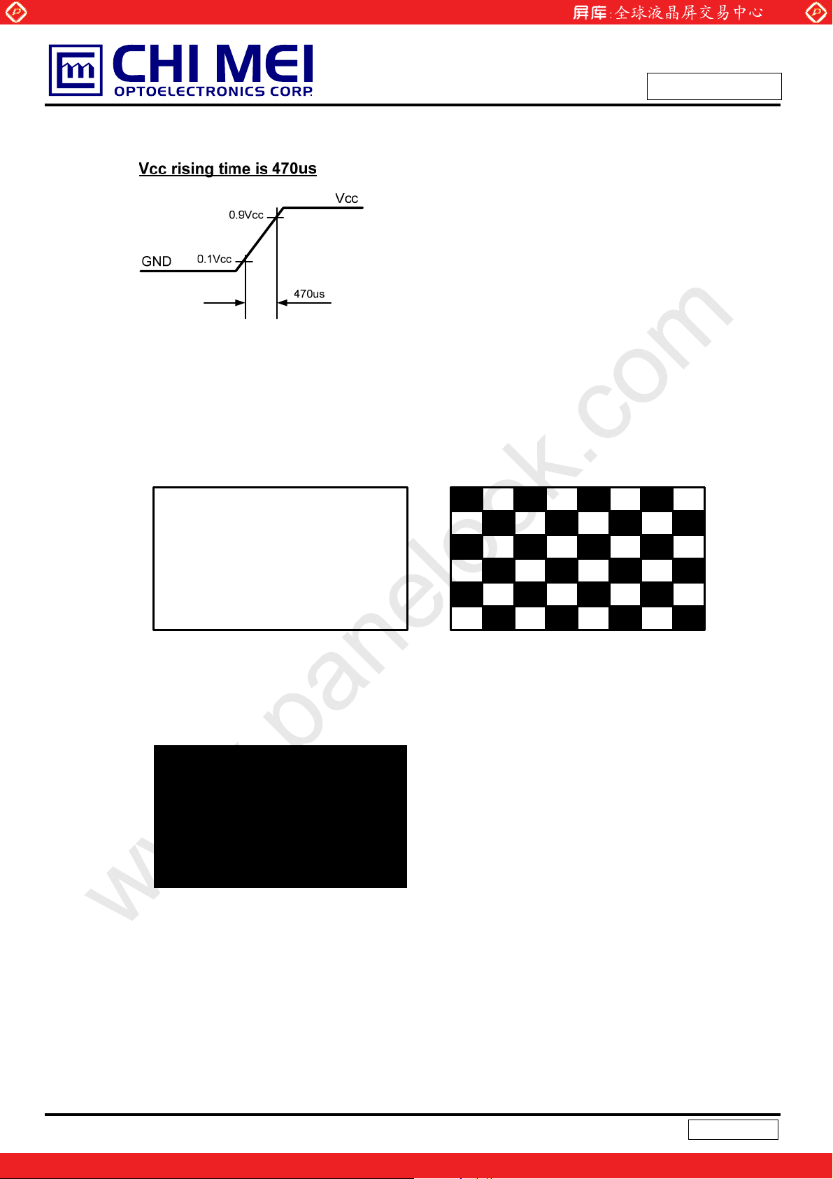
6.2 POWER ON/OFF SEQUENCE
(Ta = 25 ± 2 ºC)
To prevent a latch-up or DC operation of LCD module, the power on/off sequence should follow the diagram
below.
www.panelook.com
Issue Date:Dec.28.2007
Model No.: V420H1-LH3
Preliminary
Signal Min. Typ. Max. Unit Note
T1 0.5 - 10 ms -
T2 0 - 50 ms -
T3 0 - 50 ms -
T4 500 - - ms -
T5 500 - - ms -
T6 100 - - ms -
Note.
The supply voltage of the external system for the module input should follow the definition of Vcc.
Apply the lamp voltage within the LCD operation range. When the backlight turns on before the LCD operation or
the LCD turns off before the backlight turns off, the display may momentarily become abnormal screen.
In case of VCC is in off level, please keep the level of input signals on the low or high impedance.
T4 should be measured after the module has been fully discharged between power off and on period.
Interface signal shall not be kept at high impedance when the power is on.
24
One step solution for LCD / PDP / OLED panel application: Datasheet, inventory and accessory!
Version 1.0
www.panelook.com
Page 25

Global LCD Panel Exchange Center
7. OPTICAL CHARACTERISTICS
7.1 TEST CONDITIONS
Item Symbol Value Unit
www.panelook.com
Issue Date:Dec.28.2007
Model No.: V420H1-LH3
Preliminary
Ambient Temperature Ta
Ambient Humidity Ha
Supply Voltage VCC 12 V
Input Signal According to typical value in "3. ELECTRICAL CHARACTERISTICS"
Lamp Current IL
Oscillating Frequency (Inverter) FW
Vertical Frame Rate Fr 100 Hz
The LCD module should be stabilized at given temperature for 1 hour to avoid abrupt temperature change during
measuring. In order to stabilize the luminance, the measurement should be executed after lighting backlight for 1
hour in a windless room.
LCD Module
LCD Panel
Center of the Screen
25r2
50r10
115r10
45r2
Display Color Analyzer
oC
%RH
mA
KHz
(Minolta CA210)
Light Shield Room
(Ambient Luminance < 2 lux)
25
One step solution for LCD / PDP / OLED panel application: Datasheet, inventory and accessory!
Version 1.0
www.panelook.com
Page 26

Global LCD Panel Exchange Center
7.2 OPTICAL SPECIFICATIONS
The relative measurement methods of optical characteristics are shown in 7.2. The following items should be
measured under the test conditions described in 7.1 and stable environment shown in Note (6).
Item Symbol Condition Min. Typ. Max. Unit Note
Contrast Ratio CR (1600) (1800) - Note (2)
www.panelook.com
Issue Date:Dec.28.2007
Model No.: V420H1-LH3
Preliminary
Response Time
Center Luminance of White LC (400) (500) cd/m2Note (4)
White Variation
Cross Talk CT (4) % Note (5)
Red
Green
Color
Chromaticity
Viewing Angle
Blue
White
Color Gamut C.G
Horizontal
Vertical
Gray to
gray
GW
Rx (0.644) -
Ry (0.333) -
Gx
Gy
Bx
By
Wx
Wy
Tx+
Tx-
TY+
TY-
Tx=0q, Ty =0q
Viewing angle
at normal direction
CRt20
(4.0) (8.0) ms Note (3)
(1.3) - Note (7)
(0.272)
Typ.
-0.03
(68) (72) % NTSC
(0.591)
(0.143)
(0.070)
(0.280)
(0.285)
80 88
80 88
80 88
80 88
Typ.
+0.03
-
-
-
-
-
-
Deg. Note (1)
Gamma - (2.2) -
Note (1) Definition of Viewing Angle (Tx, Ty):
Viewing angles are measured by Eldim EZ-Contrast 160R
26
Version 1.0
One step solution for LCD / PDP / OLED panel application: Datasheet, inventory and accessory!
www.panelook.com
Page 27

Global LCD Panel Exchange Center
Note (2) Definition of Contrast Ratio (CR):
The contrast ratio can be calculated by the following expression.
Contrast Ratio (CR) = L255/L0
L255 : Luminance of gray level 255
L0 : Luminance of gray level 0
CR = CR (5), where CR (X) is corresponding to the Contrast Ratio of the point X at the figure in Note (7).
Note (3) Definition of Gray-to-Gray Switching Time:
www.panelook.com
Issue Date:Dec.28.2007
Model No.: V420H1-LH3
Preliminary
The driving signal means the signal of luminance 0%, 20%, 40%, 60%, 80%, 100%.
Gray to gray average time means the average switching time of luminance 0%, 20%, 40%, 60%, 80%,
100% to each other.
Note (4) Definition of Luminance of White (LC, LAVE):
Measure the luminance of gray level 255 at center point and 5 points
LC = L (5), where L (X) is corresponding to the luminance of the point X at the figure in Note (7).
Note (5) Definition of Cross Talk (CT):
CT = | YB – YA | / YA u 100 (%)
Where:
YA = Luminance of measured location without gray level 0 pattern (cd/m2)
YB = Luminance of measured location with gray level 0 pattern (cd/m2)
27
One step solution for LCD / PDP / OLED panel application: Datasheet, inventory and accessory!
Version 1.0
www.panelook.com
Page 28

Global LCD Panel Exchange Center
Note (6) Definition of White Variation (GW):
Measure the luminance of gray level 255 at 5 points
www.panelook.com
Issue Date:Dec.28.2007
Model No.: V420H1-LH3
Preliminary
GW = Maximum [L (1), L (2), L (3), L (4), L (5)] / Minimum [L (1), L (2), L (3), L (4), L (5)]
28
One step solution for LCD / PDP / OLED panel application: Datasheet, inventory and accessory!
Version 1.0
www.panelook.com
Page 29

Global LCD Panel Exchange Center
www.panelook.com
Issue Date:Dec.28.2007
Model No.: V420H1-LH3
Preliminary
8. PRECAUTIONS
8.1 ASSEMBLY AND HANDLING PRECAUTIONS
[ 1 ] Do not apply rough force such as bending or twisting to the module during assembly.
[ 2 ] It is recommended to assemble or to install a module into the user’s system in clean working areas. The
dust and oil may cause electrical short or worsen the polarizer.
[ 3 ] Do not apply pressure or impulse to the module to prevent the damage of LCD panel and Backlight.
[ 4 ] Always follow the correct power-on sequence when the LCD module is turned on. This can prevent the
damage and latch-up of the CMOS LSI chips.
[ 5 ] Do not plug in or pull out the I/F connector while the module is in operation.
[ 6 ] Do not disassemble the module.
[ 7 ] Use a soft dry cloth without chemicals for cleaning, because the surface of polarizer is very soft and easily
scratched.
[ 8 ] Moisture can easily penetrate into LCD module and may cause the damage during operation.
[ 9 ] When storing modules as spares for a long time, the following precaution is necessary.
[ 9.1 ] Do not leave the module in high temperature, and high humidity for a long time. It is highly
recommended to store the module with temperature from 0 to 35кat normal humidity without
condensation.
[ 9.2 ] The module shall be stored in dark place. Do not store the TFT-LCD module in direct sunlight or
fluorescent light.
[ 10 ] When ambient temperature is lower than 10ºC, the display quality might be reduced. For example, the
response time will become slow, and the starting voltage of CCFL will be higher than that of room
temperature.
8.2 SAFETY PRECAUTIONS
[ 1 ] The startup voltage of a Backlight is approximately 1000 Volts. It may cause an electrical shock while
assembling with the inverter. Do not disassemble the module or insert anything into the Backlight unit.
[ 2 ] If the liquid crystal material leaks from the panel, it should be kept away from the eyes or mouth. In case of
contact with hands, skin or clothes, it has to be washed away thoroughly with soap.
[ 3 ] After the module’s end of life, it is not harmful in case of normal operation and storage.
29
One step solution for LCD / PDP / OLED panel application: Datasheet, inventory and accessory!
Version 1.0
www.panelook.com
Page 30

Global LCD Panel Exchange Center
9. DEFINITION OF LABELS
9.1 CMO MODULE LABEL
The barcode nameplate is pasted on each module as illustration, and its definitions are as following explanation.
www.panelook.com
Issue Date:Dec.28.2007
Model No.: V420H1-LH3
Preliminary
CHI MEI
OPTOELECTRONICS
Model Name: V420H1-LH3
Revision: Rev. XX, for example: A0, A1… B1, B2… or C1, C2…etc.
Serial ID: X X X X X X X Y M D L N N N N
V420H1 -LH3 Rev. XX
X X X X X X X Y M D L N N N N
Serial No.
Product Line
Year, Month, Date
CMO Internal Use
CMO Internal Use
Revision
E207943
MADE IN TAIWAN
RoHS
CMO Internal Use
Serial ID includes the information as below:
Manufactured Date:
Year: 0~9, for 2000~2009
Month: 1~9, A~C, for Jan. ~ Dec.
Day: 1~9, A~Y, for 1st to 31st, exclude I ,O, and U.
Revision Code: Cover all the change
Serial No.: Manufacturing sequence of product
Product Line: 1 -> Line1, 2 -> Line 2, …etc.
30
One step solution for LCD / PDP / OLED panel application: Datasheet, inventory and accessory!
Version 1.0
www.panelook.com
Page 31

Global LCD Panel Exchange Center
10. PACKAGING
10.1 PACKAGING SPECIFICATIONS
3 LCD TV modules / 1 Box
Box dimensions: 1080(L) X 282 (W) X 685(H)
Weight: approximately 45Kg (3 modules per box)
10.2 PACKAGING METHOD
Figures 10-1 and 10-2 are the packing method.
LCD TV Module
www.panelook.com
Issue Date:Dec.28.2007
Model No.: V420H1-LH3
Preliminary
3pcs Drier
Cushion(Bottom)
Anti-static Bag
Carton
PP Belt
Carton Label
Figure.10-1 packing method
31
One step solution for LCD / PDP / OLED panel application: Datasheet, inventory and accessory!
Version 1.0
www.panelook.com
Page 32

Global LCD Panel Exchange Center
www.panelook.com
Issue Date:Dec.28.2007
Model No.: V420H1-LH3
Preliminary
Sea / Land Transportation (40ft HQ Container)
(L1000*50*50mm)
Film
(L1250*50*50mm)
Air Transportation &
Sea / Land Transportation (40ft Container)
(L1000*50*50mm)
Film
(L1150*W1085*H140mm)
(L1250*50*50mm)
Figure.10-2 Packing method
32
One step solution for LCD / PDP / OLED panel application: Datasheet, inventory and accessory!
Version 1.0
www.panelook.com
Page 33

Global LCD Panel Exchange Center
11. MECHANICAL CHARACTERISTICS
www.panelook.com
Issue Date:Dec.28.2007
Model No.: V420H1-LH3
Preliminary
ڻႝηިҽԖϦљ
%*+/'+
33
One step solution for LCD / PDP / OLED panel application: Datasheet, inventory and accessory!
Version 1.0
www.panelook.com
Page 34

Global LCD Panel Exchange Center
www.panelook.com
Issue Date:Dec.28.2007
Model No.: V420H1-LH3
Preliminary
ڻႝηިҽԖϦљ
%*+/'+
34
One step solution for LCD / PDP / OLED panel application: Datasheet, inventory and accessory!
Version 1.0
www.panelook.com
Page 35

Global LCD Panel Exchange Center
www.panelook.com
Issue Date:Dec.28.2007
Model No.: V420H1-LH3
Preliminary
ڻႝηިҽԖϦљ
%*+/'+
35
One step solution for LCD / PDP / OLED panel application: Datasheet, inventory and accessory!
Version 1.0
www.panelook.com
 Loading...