

Page 1
Issue Date: Oct.27.2005
Model No.:V420H1-L05
Preliminary
TFT LCD Preliminary Specification
MODEL NO.: V420H1 - L05
陳永一
LCD TV Head Division
郭振隆
李汪洋
藍文錦
嚴逸塵 林孟慧
林文聰
1
The inform ation described in this t echnical specification is tentative and it is pos sible to be changed wit hout prior
notice. Please contact CMO ’s representative while your product design is based on this specification.
Version1.0
Page 2

Issue Date: Oct.27.2005
Model No.:V420H1-L05
Preliminary
- CONTENTS -
1. GENERAL DESCRIPTION
1.1 OVERVIEW
1.2 FEATURES
1.3 APPLICATION
1.4 GENERAL SPECIFICATIONS
1.5 MECHANICAL SPECIFICATIONS
2. ABSOLUTE MAXIMUM RATINGS
2.1 ABSOLUTE RATINGS OF ENVIRONMENT
2.2 ELECTRICAL ABSOLUTE RATINGS
2.2.1 TFT LCD MODULE
2.2.2 BACKLIGHT INVERTER UNIT
3. ELECTRICAL CHARACTERISTICS
3.1 TFT LCD MODULE
3.2 BACKLIGHT UNIT
3.2.1 CCFL
3.2.2 INVERTER CHARACTERISTICS
3.2.3 INVERTER INTERTFACE CHARACTERISTICS
(Cold Cathode Fluorescent Lamp) CHARACTERISTICS
4. BLOCK DIAGRAM
4.1 TFT LCD MODULE
5. V420H1-L05 LCD INPUT TERMINAL PIN ASSIGNMENT
5.1 TFT LCD MODULE INPUT
5.2 BACKLIGHT UNIT
5.3 INVERTER UNIT
5.4 BLOCK DIAGRAM OF INTERFACE
5.5 LVDS INTERFACE
5.6 COLOR DATA INPUT ASSIGNMENT
6. INTERFACE TIMING
6.1 INPUT SIGNAL TIMING SPECIFICATIONS
6.2 POWER ON/OFF SEQUENCE
7. OPTICAL CHARACTERISTICS
7.1 TEST CONDITIONS
7.2 OPTICAL SPECIFICATIONS
8. PRECAUTIONS
8.1 ASSEMBLY AND HANDLING PRECAUTIONS
8.2 SAFETY PRECAUTIONS
9.DEFINITION OF LABELS -------------------------------------------------------29
9.1 CMO MODULE LABEL
10. MECHANICAL CHARACTERISTICS ------------------------------------------------------30
------------------------------------------------------- 3
------------------------------------------------------- 4
-------------------------------------------------------- 6
-------------------------------------------------------12
--------------------------------------------------------13
-------------------------------------------------------21
-------------------------------------------------------24
-------------------------------------------------------28
2
The inform ation described in this t echnical specification is tentative and it is pos sible to be changed wit hout prior
notice. Please contact CMO ’s representative while your product design is based on this specification.
Version1.0
Page 3
Issue Date: Oct.27.2005
Model No.:V420H1-L05
Preliminary
1. GENERAL DESCRIPTION
1.1 OVERVIEW
V420H1-L05 is a 42” TFT Liquid Crystal Display module with 20-CCFL Backlight unit and 2ch-LVDS
interface. This module s upports 1920 x 1080 HDTV form at and can display true 16.7M colors (8-bit/color).
The inverter module for backlight is built-in.
1.2 FEATURES
- High brightness (500 nits)
- High contrast ratio (1200:1)
- Fast response time (<6.5 ms)
- High color saturation (NTSC 75%)
- Full HDTV (1920 x 1080 pixels) resolution, true HDTV format
- DE (Data Enable) only mode
- LVDS (Low Voltage Differential Signaling) interface
- Optimized response time for 50/60 Hz frame rate
- Ultra wide viewing angle : Super MVA technology
- 180 degree rotation display option
1.3 AP PL ICATION
- Standard Living Room TVs.
- Public Display Application.
- Home Theater Application.
- MFM Application.
1.4 GENERAL SPECIFICA T I0NS
× Specification Unit Note
Active Area 930.24(H) x 523.26 (V) (42.02” diagonal) mm
Bezel Opening Area 938.3 (H) x 531.3 (V) mm
Driver Element a-si TFT active matrix - Pixel Number 1920x R.G.B. x 1080 pixel Pixel Pitch(Sub Pixel) 0.1615 (H) x 0.4845 (V) mm Pixel Arrangement RGB vertical stripe - Display Colors 16.7M color Display Operation Mode Transmissive mode / Normally black - -
Anti-reflective coating
Surface Treatment
Hard coating (3H)
Reflection rate : < 2%
- (2)
Note (1) Please refer to the attached drawings in chapter 9 for more information about the front and
back outlines.
(1)
Note (2) The spec of the surface treatment is temporarily for this phase. CMO reserves the rights to
change this feature.
3
The inform ation described in this t echnical specification is tentative and it is pos sible to be changed wit hout prior
notice. Please contact CMO ’s representative while your product design is based on this specification.
Version1.0
Page 4
Issue Date: Oct.27.2005
Model No.:V420H1-L05
Preliminary
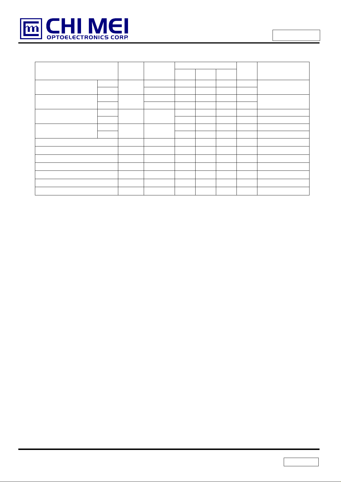
1.5 MECHA NICAL SPECIFICATIONS
Item Min. Typ. Max. Unit Note
Horizontal (H) - 983 - mm
Module Size
Note (1) Please refer to the attached drawings for more information of front and back outline dimensions.
Note (2) Module Depth does not include connectors.
Vertical (V) - 576 - mm
Depth (D) - 52.3 - mm
Weight - 16000 - g -
2. ABSOLUTE MAXIMUM RATINGS
2.1 ABSOLUTE RATINGS OF ENVIRONMENT
Item Symbol
Storage Temperature TST -20 +60 ºC (1)
Operating Ambient Te mperature TOP 0 50 ºC (1), (2)
Shock (Non-Operating) S
Vibration (Non-Operating) V
Note (1) Temperature and relative humidity range is shown in the figure below.
- (50) G (3), (5)
NOP
- 1.0 G (4), (5)
NOP
Min. Max.
Value
Unit Note
(1), (2)
(a) 90 %RH Max. (Ta ≦ 40 ºC).
(b) Wet-bulb temperature should be 39 ºC Max. (Ta > 40 ºC).
(c) No condensation.
Note (2) The maximum operating temperature is based on the test condition that the surface temperature of
display area is less than or equal to 60 ºC with LCD module alone in a temperature controlled chamber.
Thermal management should be considered in final product design to prevent the surface temperature
of display area from being over 60 ºC. The range of operating temperature may degrade in case of
improper thermal management in final product design.
Note (3) 11 ms, half sine wave, 1 time for ± X, ± Y, ± Z.
Note (4) 10 ~ 200 Hz, 10 min, 1 time each X, Y, Z.
Note (5) At testing Vibrati on a nd Sh oc k, the fixture in holdin g th e module has to be hard an d rig id e nou gh s o t ha t
the module would not be twisted or bent by the fixture.
4
The inform ation described in this t echnical specification is tentative and it is pos sible to be changed wit hout prior
notice. Please contact CMO ’s representative while your product design is based on this specification.
Version1.0
Page 5
2.2 ELECTRICAL ABSOLUTE RATI NGS
2.2.1 TFT LCD MODULE
Issue Date: Oct.27.2005
Model No.:V420H1-L05
Preliminary
Item Symbol
Min. Max.
Power Supply Voltage VCC -0.3 20 V
Logic Input Voltage VIN -0.3 3.6 V
Value
Unit Note
(1)
2.2.2 BACKLIGHT INVERTER UNIT
Item Symbol
Lamp Voltage VW
Power Supply Voltage VBL 0 30 V
Control Signal Level
Note (1) Perm anent dam age to the devic e m ay occur if m aximum values are excee ded. Func tion oper ation
should be restricted to the conditions described under Normal Operating Conditions.
Note (2) No moisture condensation or freezing.
Note (3)The control signals include On/Off Control, Internal PWM Control, External PWM Control and
Internal/External PWM Selection.
-
Value
Min. Max.
-
-0.3 7 V
3000 V
Unit Note
RMS
(1)
(1), (3)
5
The inform ation described in this t echnical specification is tentative and it is pos sible to be changed wit hout prior
notice. Please contact CMO ’s representative while your product design is based on this specification.
Version1.0
Page 6
Issue Date: Oct.27.2005
Model No.:V420H1-L05
Preliminary
3. ELECTRICAL CHARACTERISTICS
3.1 TFT LCD MODULE (Ta = 25 ± 2 ºC)
Parameter Symbol
Power Supply Voltage VCC
Min. Typ. Max.
10.8 12 13.2
16.2 18 19.8
Power Supply Ripple Voltage VRP - - 350 mV
Rush Current I
3.0 - 4.0 A (2)
RUSH
White - 1.0 - A
I
CC
- 0.8 - A
I
CC
- 1.0 - A
V
- - +100 mV
LVTH
V
-100 - - mV
LVTL
1.125 1.25 1.375 V
LVC
- 100 - ohm
T
Power Supply Current
Differential Input High
LVDS
Interface
Threshold Voltage
Differential Input Low
Threshold Voltage
Common Input Voltage V
Terminating Resistor R
Black - 0.6 - A
Vertical Str i pe
White - 1.4 - A
Black - 0.8 - A
Vertical Str i pe
Input High Threshold Voltage VIH 2.7 - 3.3 V CMOS
interface
Input Low Threshold Voltage V
0 - 0.7 V
IL
Note (1) The module should be always operated within the above ranges.
Value
Unit Note
V (1)
(3)
(4)
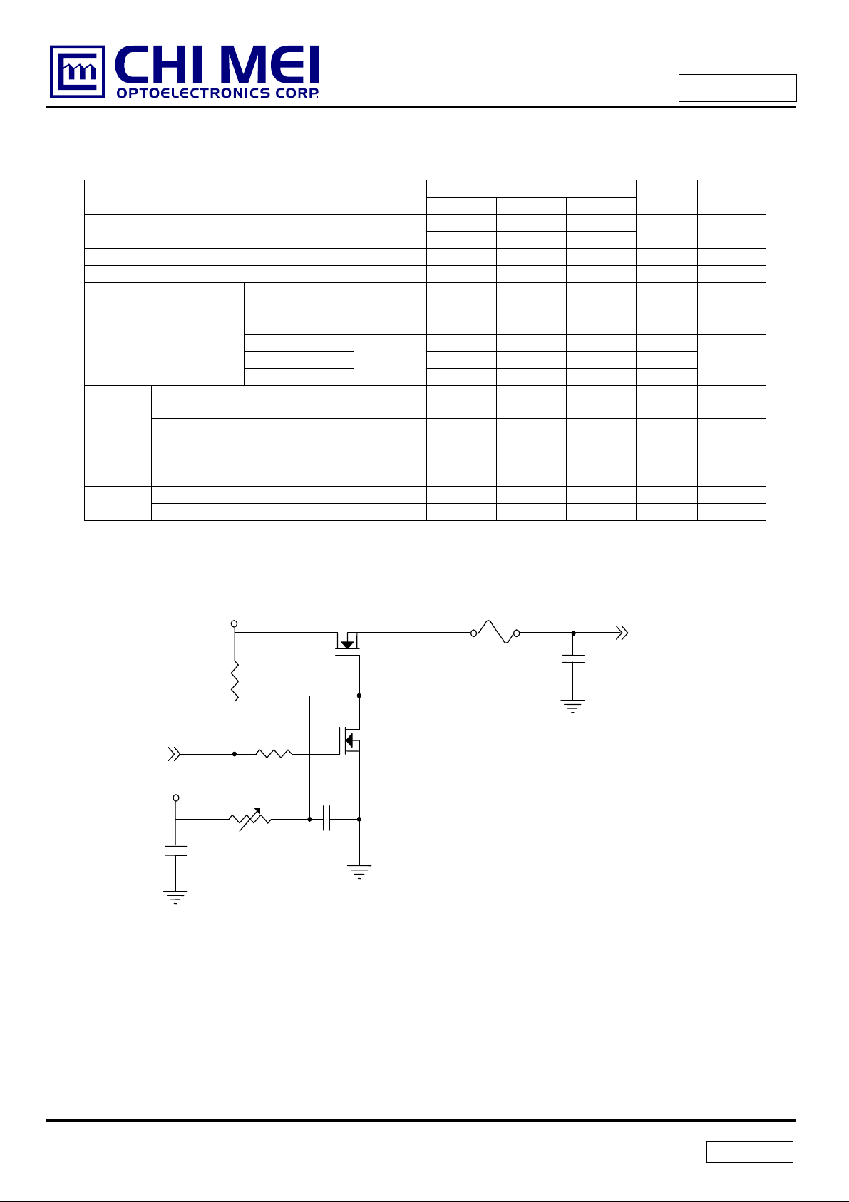
Note (2) Measurement condition:
(High to Low)
(Control Signal)
SW
+24V
C1
1uF
Vcc
VR1
R1
47K
R2
47K
1K
Q1 2SK1475
C2
0.01uF
Q2
2SK1470
FUSE
C3
1uF
Vcc
(LCD Module Input)
Note (3)&(4) T he specified po wer supply cur rent is under the conditions at Vcc = 18 V(Note(3)), Vcc = 12V( Note(4)),
6
The inform ation described in this t echnical specification is tentative and it is pos sible to be changed wit hout prior
notice. Please contact CMO ’s representative while your product design is based on this specification.
Version1.0
Page 7
Issue Date: Oct.27.2005
Model No.:V420H1-L05
Preliminary
Vcc rising time is 470us
Vcc
0.9Vcc
0.1Vcc
GND
470us
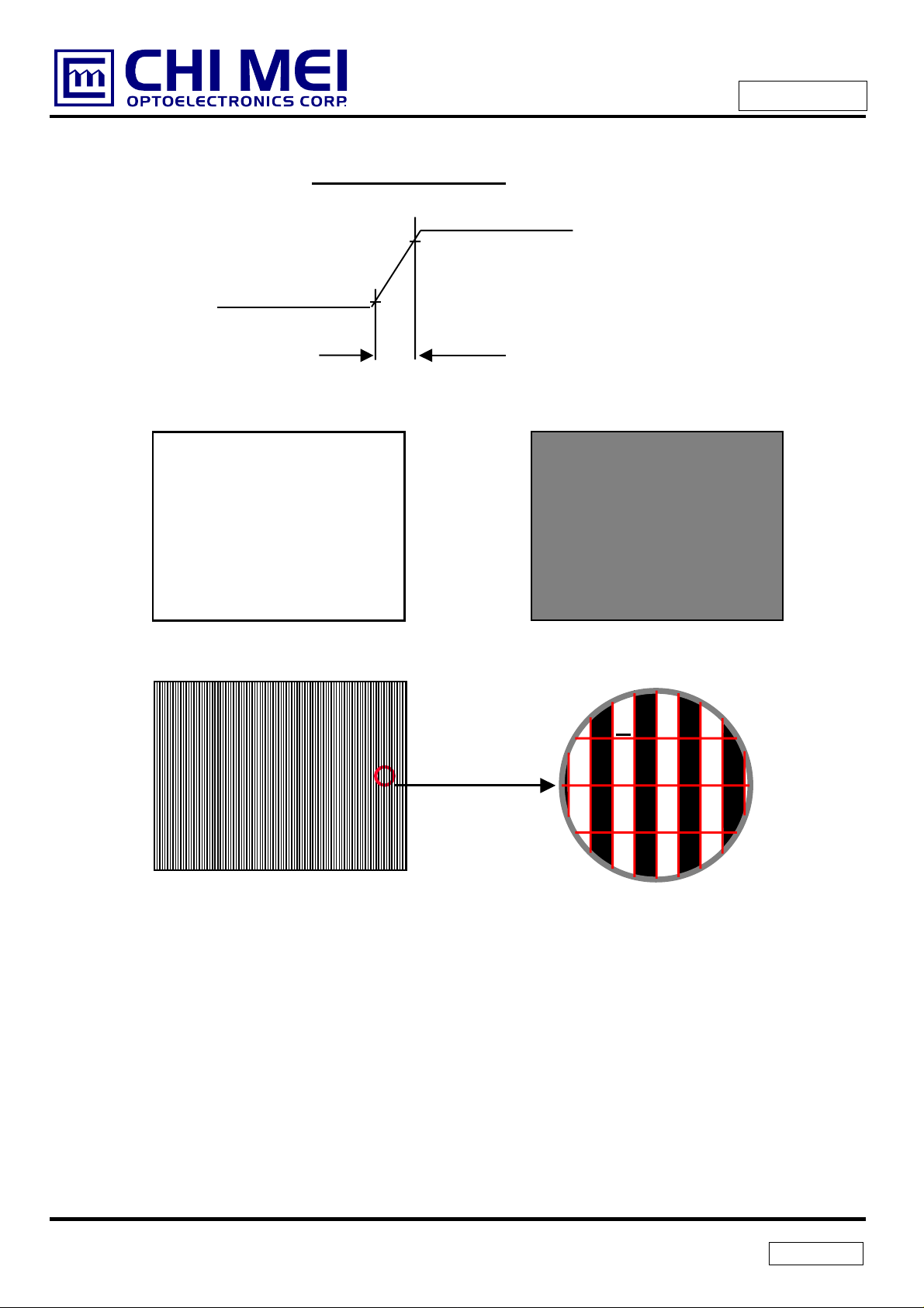
Ta = 25 ± 2 ºC, fv = 60 Hz, whereas a power dissipation check pattern below is displayed.
a. White Pattern
Active Area
c. Vertical Stri pe Pat t ern
b. Black Pattern
Active Area
G
R
R
B
G
R
B
G
R R
G
B
B
B
B
R
R
R
G
G
G
G
B
B
B
B
R
R
Active Area
7
The inform ation described in this t echnical specification is tentative and it is pos sible to be changed wit hout prior
notice. Please contact CMO ’s representative while your product design is based on this specification.
Version1.0
Page 8
Issue Date: Oct.27.2005
Model No.:V420H1-L05
Preliminary
3.2 BACKLIGHT UNIT
3.2.1 CCFL (Cold Cathode Fluorescent Lamp) CHARACTERISTICS (Ta = 25 ± 2 ºC)
Value
Unit Note
-
RMS
(1)
RMS
(2), Ta = 0 ºC
RMS
(2), Ta = 25 ºC
RMS
Parameter Symbol
Min. Typ. Max.
Lamp Input Voltage VL - 1355 - V
Lamp Current IL 6.0 6.5 7.0 mA
Lamp Turn On Voltage VS
- - 2270 V
- - 1910 V
Operating Frequency FL 40 - 70 KHz (3)
Lamp Life Time LBL 50,000 - - Hrs (4)
3.2.2 INVERTER CHARACTERISTICS (
Parameter Symbol
Power Consumption P
- 187 224 W (5), IL = 6.5mA
BL
Ta = 25 ± 2 ºC)
Value
Min. Typ. Max.
Unit Note
Power Supply Voltage VBL 22.8 24 25.2 VDC
Power Supply Current IBL - 7.8 - A Non Dimming
Input Ripple Noise - - - 500 mV
Backlight Turn on
Voltage
V
BS
2270
1910 - - V
- -
VBL=22.8V
P-P
V
Ta = 0 ºC
RMS
Ta = 25 ºC
RMS
Oscillating Frequency FW 47 50 53 kHz
Dimming frequency FB 150 160 170 Hz
Minimum Duty Ratio D
- 20 - %
MIN
Note (1) Lamp current is measured by utilizing high frequency current meters as shown below:
Note (2) The lamp starting voltage V
should be applied to the lamp for more than 1 second after startup.
S
Otherwise the lamp may not be turned on.
Note (3) The lamp frequency may produce interference with horizontal synchronous frequency of the
display input signals, and it may result in line flow on the display. In order to avoid interference, the
lamp frequency should be detached from the horizontal synchronous frequency and its harmonics
as far as possible.
Note (4) The life time of a lamp is defined as when the brightness is larger than 50% of its original value and
the effective dischar ge le ngth is long er th an 80% of its origi nal length (Eff ective di sc harge leng th is
defined as an area that has equal to or more than 70% brightness compared to the brightness at
the center point of lam p.) as the time in which it contin ues to op er ate u nder t he c o ndit io n at Ta = 25
±2℃ and I
Note ( 5) The power s upply capacity should be hi gher than the total invert er power consum ption P
= 6.0~ 7.0mArms.
L
. Since
BL
the pulse width modulation (PWM) mode was applied for backlight dimming, the driving current
changed as PW M duty on and off. The transient response of power sup ply should be considere d
for the changing loading when inverter dimming.
8
The inform ation described in this t echnical specification is tentative and it is pos sible to be changed wit hout prior
notice. Please contact CMO ’s representative while your product design is based on this specification.
Version1.0
Page 9
Issue Date: Oct.27.2005
Model No.:V420H1-L05
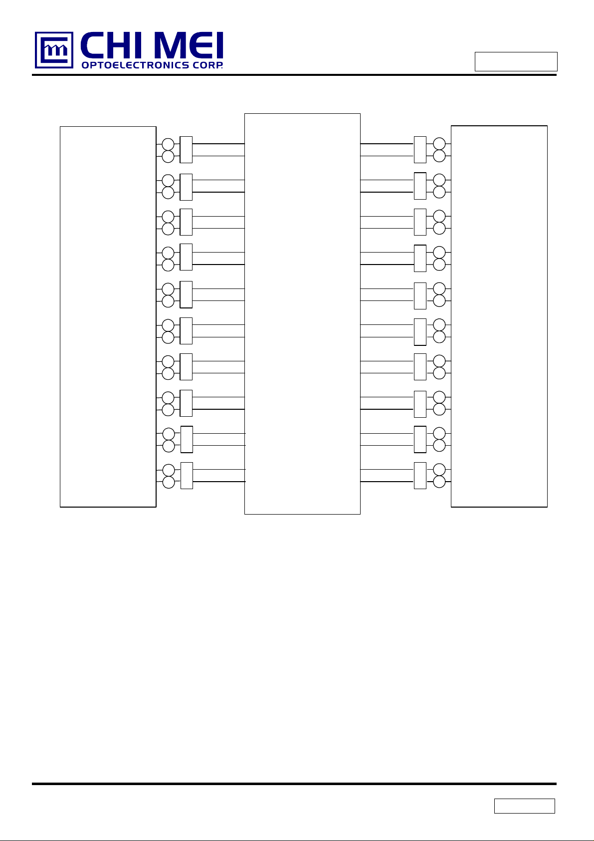
Preliminary
Inverter
(Master)
A
A
A
A
A
A
A
A
A
A
A
A
A
A
A
A
HV (White -)
1
HV(Pink -)
2
HV (White +)
1
HV(Pink +)
2
HV (White -)
1
HV(Pink -)
2
HV (White +)
1
HV(Pink +)
2
HV (White -)
1
HV(Pink -)
2
HV (White +)
1
HV(Pink +)
2
HV (White -)
1
HV(Pink -)
2
HV (White +)
1
HV(Pink +)
2
LCD Module
HV (Pink +)
HV (White +)
HV (Pink -)
HV (White -)
HV (Pink +)
HV (White +)
HV (Pink -)
HV (White -)
HV (Pink +)
HV (White +)
HV (Pink -)
HV (White -)
HV (Pink +)
HV (White +)
HV (Pink -)
HV (White -)
A
1
2
A
A
1
2
A
A
1
2
A
A
1
2
A
A
1
2
A
A
1
2
A
A
1
2
A
A
1
2
A
Inverter
(Slavor)
A
A
A
A
HV(Blue -)
1
HV (Pink -)
2
HV(Blue +)
1
HV (Pink +)
2
HV (Pink +)
HV (White +)
HV (Pink -)
HV (White -)
A
1
2
A
A
1
2
A
9
The inform ation described in this t echnical specification is tentative and it is pos sible to be changed wit hout prior
notice. Please contact CMO ’s representative while your product design is based on this specification.
Version1.0
Page 10
Issue Date: Oct.27.2005
y
y
Model No.:V420H1-L05
Preliminary
3.2.3 INVERTER INTERTFACE CHARACTERISTICS
Parameter Symbol
On/Off Control Voltage
Select Voltage
Voltage
Voltage
ON
OFF
HI
LO
MAX
MIN
HI 2.0
LO
V
V
V
V
BLON
SEL
IPWM
EPWM
Control Signal Rising Time Tr
Control Signal Falling Time Tf
PWM Signal Rising Time T
PWM Signal Falling Time T
PWMR
PWMF
Input impedance RIN
Test
Condition
-
-
-
-
V
SEL
V
SEL
- - -
- - -
- - -
- - -
-
Min. Typ. Max.
= L
= H
BLON Delay Time Ton - 1 - - ms
BLON Off Time T
- 1 - - ms
off
Note (1) The SEL signal sh ould be val id before b ack light turns on by BLO N signal . It is in hibited t o change
Value
2.0
0
2.0
--
0
- -
-
0
1
Unit Note
-
-
5.0 V
0.8 V
5.0 V Internal/External PWM
-
0.8 V
3.0 V maximum duty ratioInternal PWM Control
0
-
-
-
5.0 V duty on External PWM Control
0.8 V dut
V minimum dut
100 ms
100 ms
50 us
50 us
- - MΩ
ratio
off
the internal/external PWM selection (SEL) during backlight turn on period.
Note (2) The power sequence and control signal timing are shown in the following figure.
Note (3) The power seq uence and contro l signal tim ing must follo w the figure belo w. For a certain reason,
the inverter has a possibility to be damaged with wrong power sequence and control signal
timing.
10
The inform ation described in this t echnical specification is tentative and it is pos sible to be changed wit hout prior
notice. Please contact CMO ’s representative while your product design is based on this specification.
Version1.0
Page 11

Issue Date: Oct.27.2005
Model No.:V420H1-L05
Preliminary
V
BL
V
V
V
BLON
V
SEL
EPWM
IPWM
V
0
0
0
0
0
W
2.0V
0.8V
2.0V
0.8V
2.0V
0.8V
3.0V
on1
T
Backlight on duration
r
T
Ext. Dimming Function
T
PWMR
T
PWMF
T
f
Int. Dimming Function
T
off1
External
PWM
Period
External
PWM Duty
100%
Minimun
Duty
11
The inform ation described in this t echnical specification is tentative and it is pos sible to be changed wit hout prior
notice. Please contact CMO ’s representative while your product design is based on this specification.
Version1.0
Page 12

4. BLOCK DIAGRAM OF INTERFACE
)
4.1 TFT LCD MODULE
Issue Date: Oct.27.2005
Model No.:V420H1-L05
Preliminary
ERX0(+/-)
ERX1(+/-)
ERX2(+/-)
ERX3(+/-)
ECLK(+/-)
DCLK(+/-)
DE
ORX0(+/-)
ORX1(+/-)
ORX2(+/-)
ORX3(+/-)
OCLK(+/-)
INPUT CONNECTOR
(FI-R(E)51S-HF )
FRAME
BUFFER
TIMING
CONTROLLER
DC/DC CONVERTER
& REFERENCE
SCAN DRIVER
TFT LCD PANEL
(1920x3x1080)
DATA DRIVER (RSDS
VOLTAGE
Vcc
GND
CN1.
VBL
GND
SEL
E_PWM
I_PWM
BLON
INVERTER
CONNECTOR
CN1:S14B-PH-SM3-TB
(D)(LF) or equivalent
(Master)
GENERATOR
CN3-CN22:SM02 (12.0)B-BHS-1-TB(LF)(JST)
or equivalent
BACKLIGHT
UNIT
INVERTER
CONNECTOR
CN2:S12B-PH-SM3-TB
(D)(LF) or equivalent
(Slave)
CN2.
VBL
GND
CN23-CN26: 53261-1060(Molex) or equivalent
12
The inform ation described in this t echnical specification is tentative and it is pos sible to be changed wit hout prior
notice. Please contact CMO ’s representative while your product design is based on this specification.
Version1.0
Page 13

Issue Date: Oct.27.2005
Model No.:V420H1-L05
Preliminary
5. INPUT TERMINAL PIN ASSIGNMENT
5.1 TFT LCD Module Input
Connector part no. : FI-R(E)51S-HF (JAE) or equivalent.
Pin Name Description Note
1 GND Ground
2 N.C. No Connection
3 N.C. No Connection
4 N.C. No Connection
5 N.C. No Connection
6 N.C. No Connection
7 NC No Connection
8 RPF Display Rotation (1)
9 ODSEL
10 LCS Low color shift (3)
11 GND Ground
12 ORX0- Odd pixel, Negative LVDS differential data input. Channel 0
13 ORX0+ Odd pixel, Positive LVDS differential data input. Channel 0
14 ORX1- Odd pixel, Negative LVDS differential data input. Channel 1
15 ORX1+ Odd pixel, Positive LVDS differential data input. Channel 1
16 ORX2- Odd pixel, Negative LVDS differential data input. Channel 2
17 ORX2+ Odd pixel, Positive LVDS differential data input. Channel 2
18 GND Ground
19 OCLK- Odd pixel, Negative LVDS differ ential clock input.
20 OCLK+ Odd pixel, Positive LVDS differential clock input.
21 GND Ground
22 ORX3- Odd pixel, Negative LVDS differential data input. Channel 3
23 ORX3+ Odd pixel, Positive LVDS differential data input. Channel 3
24 N.C. No Connection
25 N.C. No Connection
26 N.C. No Connection
27 N.C. No Connection
28 ERX0- Even pixel, Neg ative LVDS differential data input. Channel 0
29 ERX0+ Even pixel, Positive LVDS differential data input. Channel 0
30 ERX1- Even pixel, Neg ative LVDS differential data input. Channel 1
31 ERX1+ Even pixel, Positive LVDS differential data input. Channel 1
32 ERX2- Even pixel, Neg ative LVDS differential data input. Channel 2
33 ERX2+ Even pixel, Positive LVDS differential data input. Channel 2
34 GND Ground
35 ECLK- Even pixel, Neg ative LVDS differential clock input.
36 ECLK+ Even pixel, Positive LVDS differential clock input.
37 GND Ground
38 ERX3- Even pixel, Neg ative LVDS differential data input. Channel 3
39 ERX3+ Even pixel, Positive LVDS differential data input. Channel 3
40 N.C. No Connection
41 N.C. No Connection
42 N.C. No Connection
43 N.C. No Connection
44 GND Ground
45 GND Ground
Overdrive Lookup Table Selection
13
The inform ation described in this t echnical specification is tentative and it is pos sible to be changed wit hout prior
notice. Please contact CMO ’s representative while your product design is based on this specification.
(4)
(2)
(4)
(4)
Version1.0
Page 14

Issue Date: Oct.27.2005
Model No.:V420H1-L05
Preliminary
46 GND Ground
47 GND Ground
48 VCC Power input (+12V or +18.0V)
49 VCC Power input (+12V or +18.0V)
50 VCC Power input (+12V or +18.0V)
51 VCC Power input (+12V or +18.0V)
Note (1) Low : normal display (default), High : display with 180 degree rotation
Note (2) Overdrive lookup table selection. The overdrive lookup table should be selected in
accordance to the frame rate to optimize image quality.
ODSEL Note
L Lookup table was optimized for 60 Hz frame rate.
H Lookup table was optimized for 50 Hz frame rate.
Note (3) Low : normal display (default), High : Low Color Shift function enable.
Note (4) Reserved for interval use. Left it open.
5.2 BACKLIGHT UNIT
The pin configuration for the housing and the leader wire is shown in the table below.
Pin Name Description Wire Color
1 HV High Voltage Pink
2 HV High Voltage White
Note (1) The backlight interface housing for high voltage side is a model BHR-04VS-1, manufactured by JST.
The mating header on inverter part number is SM02(12.0)B-BHS-1-TB(LF).
1 HV(White)
2 HV(Pink)
1 HV(White)
2 HV(Pink)
1 HV(White)
2 HV(Pink)
CN3-CN22: BHR-04VS-1 (JST).
1 HV(Pink)
1 HV(Pink)
2 HV(White)
2 HV(White)
1 HV(Pink)
2 HV(White)
14
The inform ation described in this t echnical specification is tentative and it is pos sible to be changed wit hout prior
notice. Please contact CMO ’s representative while your product design is based on this specification.
Version1.0
Page 15

5.3 INVERTER UNIT
CN1 (Header): S14B-PH-SM3-TB (D)(LF)(JST) or equivalent.
Pin No. Symbol Description
1
2
3
4
5
6
7
8
9
10
11 SEL
12 E_PWM
13 I_PWM
14 BLON Backlight on/off control
VBL +24V
GND GND
Internal/external PWM selection
High : external dimming
Low : internal dimming
External PWM control signal
E_PWM should be connected to ground when internal PWM was selected
(SEL = Low).
Internal PWM Control Signal
I_PWM should be connected to ground when external PWM was selected
(SEL = High).
power input
DC
Issue Date: Oct.27.2005
Model No.:V420H1-L05
Preliminary
CN2 (Header): S12B-PH-SM3-TB (D)(LF)(JST) or equivalent.
Pin No. Symbol Description
1
2
3
4
5
6
7
8
9
10
11
12 NC NC
CN3- CN22 (Header): SM02(12.0)B-BHS-1-TB (LF)(JST) or equivalent
Pin No. Symbol Description
1
2
VBL +24V
GND GND
NC NC
CCFL HOT
CCFL HOT
CCFL high voltage
CCFL high voltage
power input
DC
15
The inform ation described in this t echnical specification is tentative and it is pos sible to be changed wit hout prior
notice. Please contact CMO ’s representative while your product design is based on this specification.
Version1.0
Page 16

CN23-CN26 (Header): 53261-1060(Molex) or equivalent
Pin No. Symbol Description
1 Board to Board
2 Board to Board
3 Board to Board
4 Board to Board
5 Board to Board
6 Board to Board
7 Board to Board
8 Board to Board
9 Board to Board
10
Note (1) Floating of any control signal is not allowed.
Control
Signal
Board to Board
Issue Date: Oct.27.2005
Model No.:V420H1-L05
Preliminary
16
The inform ation described in this t echnical specification is tentative and it is pos sible to be changed wit hout prior
notice. Please contact CMO ’s representative while your product design is based on this specification.
Version1.0
Page 17

5.4 BLOCK DIAGRAM OF INTERFACE
G0-EG
0
G0-EG
0
0
ORx0
O
p
OG0
OB0
CLK
OG0
OB0
CNF1
Issue Date: Oct.27.2005
Model No.:V420H1-L05
Preliminary
ERx0+
ER0-ER7
E
EB
7
-EB7
DE
OR0-OR7
-OG7
-OB7
D
TxIN
PLL
ERx
ERx1+
ERx1-
ERx2+
ERx2-
ERx3+
ERx3-
ECLK+
Host
Graphics
Controller
ORx0+
ORx1+
ORx1-
51Ω
-
100pF
51Ω
51Ω
100pF
51Ω
51Ω
100pF
51Ω
51Ω
100pF
51Ω
RxOUT
ER0-ER7
E
-EB7
EB
DE
OR0-OR7
-OG7
7
-OB7
51Ω
-
100pF
51Ω
PLL
DCLK
Timing
51Ω
51Ω
51Ω
100pF
100
F
-
Controller
ORx2+
Rx2-
ORx3+
ORx3-
51Ω
100pF
51Ω
51Ω
100pF
51Ω
PLL
OCLK+
51Ω
-
100pF
51Ω
PLL
L VDS Transmitter
THC63L VDM83A
(LVDF83A)
LVDS Receiver
17
The inform ation described in this t echnical specification is tentative and it is pos sible to be changed wit hout prior
notice. Please contact CMO ’s representative while your product design is based on this specification.
Version1.0
Page 18

ER0~ER7 : Even pixel R data
EG0~EG7 : Even pixel G data
EB0~EB7 : Even pixe l B data
OR0~OR7 : Odd pixel R data
OG0~OG7: Odd pixel G data
OB0~OB7 : Odd pixel B data
DE : Data enable signal
DCLK : Data clock signal
Notes: (1) The system must have the transmitter to drive the module.
(2) LVDS cable impedance shall be 50 ohms per signal line or about 100 ohms per twist-pair line
when it is used differentially.
(3) Two pixel data send into the module for every clock cycle. The first pixel of the frame is even pixel
Issue Date: Oct.27.2005
Model No.:V420H1-L05
Preliminary
and the second pixel is odd pixel.
18
The inform ation described in this t echnical specification is tentative and it is pos sible to be changed wit hout prior
notice. Please contact CMO ’s representative while your product design is based on this specification.
Version1.0
Page 19

5.5 LVDS INTERFACE
TRANSMITTER
SIGNAL
THC63LVDM83A
PIN INPUT Host TFT-LCD PIN OUTPUT
INTERFACE CONNECTOR
RECEIVER
THC63LVDF84A
Issue Date: Oct.27.2005
Model No.:V420H1-L05
Preliminary
TFT CONTROL
INPUT
24bit
R0
R1
R2
R3
R4
R5
G0
G1
G2
G3
G4
G5
B0
B1
B2
B3
B4
B5
DE
R6
R7
G6
G7
B6
B7
RSVD 1
RSVD 2
RSVD 3
51
52
54
55
56
3
4
6
7
11
12
14
15
19
20
22
23
24
30
50
2
8
10
16
18
25
27
28
TxIN0
TxIN1
TxIN2
TxIN3
TxIN4
TxIN6
TxIN7
TxIN8
TxIN9
TxIN12
TxIN13
TxIN14
TxIN15
TxIN18
TxIN19
TxIN20
TxIN21
TxIN22
TxIN26
TxIN27
TxIN5
TxIN10
TxIN11
TxIN16
TxIN17
TxIN23
TxIN24
TxIN25
TA OUT0+
TA OUT0-
TA OUT1+
TA OUT1-
TA OUT2+
TA OUT2-
TA OUT3+
TA OUT3-
Rx 0+
Rx 0-
Rx 1+
Rx 1-
Rx 2+
Rx 2-
Rx 3+
Rx 3-
27
29
30
32
33
35
37
38
39
43
45
46
47
51
53
54
55
1
6
7
34
41
42
49
50
2
3
5
Rx OUT0
Rx OUT1
Rx OUT2
Rx OUT3
Rx OUT4
Rx OUT6
Rx OUT7
Rx OUT8
Rx OUT9
Rx OUT12
Rx OUT13
Rx OUT14
Rx OUT15
Rx OUT18
Rx OUT19
Rx OUT20
Rx OUT21
Rx OUT22
Rx OUT26
Rx OUT27
Rx OUT5
Rx OUT10
Rx OUT11
Rx OUT16
Rx OUT17
Rx OUT23
Rx OUT24
Rx OUT25
R0
R1
R2
R3
R4
R5
G0
G1
G2
G3
G4
G5
B0
B1
B2
B3
B4
B5
DE
R6
R7
G6
G7
B6
B7
Not connect
Not connect
Not connect
DCLK 31
R0~R7: Pixel R Data (7; MSB, 0; LSB)
G0~G7: Pixel G Data (7; MSB, 0; LSB)
B0~B7: Pixel B Data (7; MSB, 0; LSB)
DE : Data enable signal
DCLK : Data clock signal
Notes: (1) RSVD (reserved) pins on the transmitter shall be “H” or “L ”.
TxCLK
IN
TxCLK OUT+
TxCLK OUT-
RxCLK IN+
RxCLK IN-
26 RxCLK OUT DCLK
19
The inform ation described in this t echnical specification is tentative and it is pos sible to be changed wit hout prior
notice. Please contact CMO ’s representative while your product design is based on this specification.
Version1.0
Page 20

Issue Date: Oct.27.2005
Model No.:V420H1-L05
Preliminary
5.7 COLOR DATA INPUT ASSIGNMENT
The brightness of each pr imary color (red, green and blu e) is bas ed on th e 8- bit gr a y scale d ata input f or th e
color. The higher the binary i nput, the brighter the co lor. T he table below provides the assi gnment of the
color versus data input.
Data Signal
Color
R7 R6 R5 R4 R3 R2 R1 R0 G7 G6 G5 G4 G3 G2 G1 G0 B7 B6 B5 B4 B3 B2 B1 B0
0
Black
Red
Green
Basic
Colors
Gray
Scale
Of
Red
Gray
Scale
Of
Green
Gray
Scale
Of
Blue
Note (1) 0: Low Level Voltage, 1: High Level Voltage
Blue
Cyan
Magenta
Yellow
White
Red (0) / Dark
Red (1)
Red (2)
:
:
Red (253)
Red (254)
Red (255)
Green (0) / Dark
Green (1)
Green (2)
:
:
Green (253)
Green (254)
Green (255)
Blue (0) / Dark
Blue (1)
Blue (2)
:
:
Blue (253)
Blue (254)
Blue (255)
0
1
1
0
0
0
0
0
0
1
1
1
1
1
1
0
0
0
0
0
0
:
:
:
:
1
1
1
1
1
1
0
0
0
0
0
0
:
:
:
:
0
0
0
0
0
0
0
0
0
0
0
0
:
:
:
:
0
0
0
0
0
0
Red Green Blue
0
0
0
0
0
0
0
0
0
0
0
0
0
0
0
0
0
0
0
0
0
0
0
0
0
0
0
0
0
0
0
0
1
1
1
1
1
1
0
0
0
0
0
1
1
1
1
1
1
1
1
0
0
0
0
0
0
1
1
1
1
1
0
0
0
0
0
0
0
0
0
0
0
0
0
0
1
1
1
1
1
1
1
1
1
1
1
1
1
0
0
0
0
0
0
1
1
1
1
1
0
0
0
0
0
0
0
0
1
1
1
1
1
1
0
0
0
0
0
1
1
1
1
1
1
1
1
1
1
1
1
1
1
1
1
1
1
1
1
1
1
1
1
1
1
1
1
1
1
1
1
1
0
0
0
0
0
0
0
0
0
0
0
0
0
0
0
0
0
0
0
0
0
0
0
0
0
0
0
0
0
0
0
0
1
0
0
0
0
0
0
0
0
0
0
0
0
0
0
0
0
0
0
0
1
0
0
0
0
:
:
:
:
:
:
:
:
:
:
:
:
:
:
:
:
:
:
:
:
:
:
:
:
:
:
:
:
:
:
:
:
:
:
:
:
:
:
0
0
0
0
0
0
0
0
0
0
0
0
0
1
0
1
1
1
1
0
0
0
0
0
0
0
0
0
0
0
0
0
0
1
1
1
1
1
0
0
0
0
0
0
0
0
0
0
0
0
0
1
1
1
1
1
1
0
0
0
0
0
0
0
0
0
0
0
0
0
0
0
0
0
0
0
0
0
0
0
0
1
0
0
0
0
0
0
0
0
0
0
0
0
0
0
0
0
0
0
0
1
0
0
0
0
0
0
0
0
0
0
0
0
:
:
:
:
:
:
:
:
:
:
:
:
:
:
:
:
:
:
:
:
:
:
:
:
:
:
:
:
:
:
:
:
:
:
:
:
:
:
0
0
0
0
0
1
0
1
1
1
1
1
1
0
0
0
0
0
0
0
0
0
0
0
0
1
1
1
1
1
1
1
0
0
0
0
0
0
0
0
0
0
0
1
1
1
1
1
1
1
1
0
0
0
0
0
0
0
0
0
0
0
0
0
0
0
0
0
0
0
0
0
0
0
0
0
0
0
0
0
0
0
0
0
0
0
0
0
0
0
0
0
0
0
0
0
0
0
0
0
0
0
0
0
0
0
0
0
0
0
0
0
0
0
:
:
:
:
:
:
:
:
:
:
:
:
:
:
:
:
:
:
:
:
:
:
:
:
:
:
:
:
:
:
:
:
:
:
:
:
:
:
1
1
1
1
1
0
0
0
0
0
0
0
0
0
0
0
0
0
0
1
1
1
1
1
0
0
0
0
0
0
0
0
0
0
0
0
0
0
1
1
1
1
1
0
0
0
0
0
0
0
0
0
0
0
0
0
0
0
0
0
0
0
0
0
0
0
1
1
1
1
1
1
1
1
1
0
0
0
1
1
1
0
0
0
0
0
0
0
0
0
:
:
:
:
:
:
0
0
0
0
0
0
0
0
0
0
0
0
0
0
0
0
0
0
:
:
:
:
:
:
0
0
0
0
0
0
0
0
0
0
0
0
1
0
0
0
1
0
:
:
:
:
:
:
1
0
1
0
1
1
1
1
1
20
The inform ation described in this t echnical specification is tentative and it is pos sible to be changed wit hout prior
notice. Please contact CMO ’s representative while your product design is based on this specification.
Version1.0
Page 21

6. INTERFACE TIMING
6.1 INPUT SIGNAL TIMING SPECIFICATIONS
The input signal timing specifications are shown as the following table and timing diagram.
Signal Item Symbol Min. Typ. Max. Unit Note
Frequency 1/Tc (60) 74 (80) MHZ -
LVDS Receiver Clock
LVDS Receiver Data
Vertical Active Display Term
Horizontal Active Disp lay Term
Note (1) (ODSEL) = (H). Please refer to 5.1 for detail information.
Input cycle to
cycle jitter
Setup Time Tlvsu 600 - - ps Hold Time Tlvhd 600 - - ps -
Frame Rate
Total Tv (1115) 1125 (1135) Th Tv=Tvd+Tvb
Display Tvd 1080 1080 1080 Th Blank Tvb (35) 45 (55) Th Total Th (2100) 2200 (2300) Tc Th=Thd+Thb
Display Thd 1920 1920 1920 Tc Blank Thb (180) 280 (380) Tc -
Trcl - - 200 ps -
Fr5 47 50 53 Hz (1)
6 57 60 63 Hz (2)
Fr
Issue Date: Oct.27.2005
Model No.:V420H1-L05
Preliminary
(2) (ODSEL) = (L). Please refer to 5.1 for detail information.
INPUT SIGNAL TIMING DIAGRAM
DE
Th
DCLK
Tc
DE
Tvd
Thb
Tv
Tvb
Thd
DATA
Valid display data ( 960 clocks)
21
The inform ation described in this t echnical specification is tentative and it is pos sible to be changed wit hout prior
notice. Please contact CMO ’s representative while your product design is based on this specification.
Version1.0
Page 22

RXCLK+/-
RXn+/-
Issue Date: Oct.27.2005
Model No.:V420H1-L05
Preliminary
LVDS INPUT INTERFACE TIMING DIAGRAM
Tc
Tlvsu
Tlvhd
1T‘
14
6.2 POWER ON/OFF SEQUENCE
To prevent a latch-up or DC operation of LCD module, the power on/off sequence should follow the
diagram below.
Power Supply
V
0.5≦T1≦10ms
0≦T
0≦T
500ms ≦T
Signals
CC
2≦50ms
3≦50ms
4
3T‘
14
0V
0V
5T‘
14
0.9 VCC
0.1V
CC
7T‘
14
2
T
9T‘
14
11T‘
14
13T‘
14
0.9 V
CC
0.1V
cc
T
3 T1
T4
VALID
Power On
Power Off
Backlight (Recommended)
500ms≦T
100ms≦T6
5
50%
5
T
Power ON/OFF Sequence
22
50%
T
6
The inform ation described in this t echnical specification is tentative and it is pos sible to be changed wit hout prior
notice. Please contact CMO ’s representative while your product design is based on this specification.
Version1.0
Page 23

Issue Date: Oct.27.2005
Model No.:V420H1-L05
Preliminary
Note.
(1) The supply voltage of the external system for the module input should follow the definition of Vcc.
(2) Apply the lamp voltage within the LCD operation range. When the backlight turns on before the
LCD operation or the LCD turns off before the backlight turns off, the display may momentarily
become abnormal screen.
(3) I n case of VCC is in off level, please keep the level of input signals on the low or high impedance.
(4) T4 should be measured after the module has been fully discharged between power off and on
period.
(5) I nterface signal shall not be kept at high impedance when the power is on.
23
The inform ation described in this t echnical specification is tentative and it is pos sible to be changed wit hout prior
notice. Please contact CMO ’s representative while your product design is based on this specification.
Version1.0
Page 24

Issue Date: Oct.27.2005
Model No.:V420H1-L05
Preliminary
7. OPTICAL CHARACTERISTICS
7.1 TEST CONDITIONS
Item Symbol Value Unit
Ambient Te mperature Ta
Ambient Humidity Ha
Supply Voltage VCC 12/18 V
Input Signal According to typical value in "3. ELECTRICAL CHARACTERISTICS"
Lamp Current IL
Oscillating Frequency (Inverter) FW
Vertical Frame Rate Fr 60 Hz
25±2
50±10
6.5±0.5
50±3
7.2 OPTICAL SPECIFICATIONS
The relative measurement methods of optical characteristics are shown in 7.2. The following items should be
o
C
%RH
mA
KHz
measured under the test conditions described in 7.1 and stable environment shown in Note (6).
Item Symbol Condition Min. Typ. Max. Unit Note
Contrast Ratio CR (1000) - Note (2)
Response Time
Center Luminance of White L
White Variation
Cross T al k CT (4) % Note (5)
Red
Green
Color
Chromaticity
Viewing
Angle
Blue
White
Color Gamut
Horizontal
Vertical
Gray to
gray
C
δW
Rx (0.651) Ry
Gx
Gy
Bx
By
Wx
Wy
θ
+
x
θ
-
x
θ
+
Y
θ
-
Y
=0°, θY =0°
θ
x
Viewing Normal Angle
CR≥20
(6.5) ms Note (3)
(500) cd/m2 Note (4)
(1.3) - Note (7)
(0.330)
0.285
0.293
Typ.
+0.03
Typ.
-0.03
(72) 75 % NTSC
(80) (88)
(80) (88)
(80) (88)
(80) (88)
(0.274)
(0.596)
(0.142)
(0.067)
-
-
Note (6)
-
-
-
-
Deg. Note (1)
24
The inform ation described in this t echnical specification is tentative and it is pos sible to be changed wit hout prior
notice. Please contact CMO ’s representative while your product design is based on this specification.
Version1.0
Page 25

Note (1) Definition of Viewing Angle (θx, θy):
T
Viewing angles are measured by Eldim EZ-Contrast 160R
Issue Date: Oct.27.2005
Model No.:V420H1-L05
Preliminary
θX- = 90º
x-
6 o’clock
θ
y- = 90º
y-
Note (2) Definition of Contrast Ratio (CR):
The contrast ratio can be calculated by the following expression.
Contrast Ratio (CR) = L255 / L0
L255: Luminance of gray level 255
Normal
θx = θy = 0º
θy- θy+
θx−
θx+
y+
12 o’clock direction
θ
y+ = 90º
x+
θX+ = 90º
L 0: Luminance of gray level 0
CR = CR (5)
CR (X) is corresponding to the Contrast Ratio of the point X at the figure in Note (7).
Note (3) Definition of Gray to Gray Switching Time :
100%
90%
Optical
Response
10%
0%
Gray to gray
switching time
Gray to gray
switching time
The driving signal means the signal of gray level 0, 63, 127, 191, and 255.
Gray to gray average time means the average switching time of gray level 0 ,63,127,191,255 to each
ime
other .
25
The inform ation described in this t echnical specification is tentative and it is pos sible to be changed wit hout prior
notice. Please contact CMO ’s representative while your product design is based on this specification.
Version1.0
Page 26

Note (4) Definition of Luminance of White (LC, L
A
(
)
A
(
)
(
)
Measure the luminance of gray level 255 at center point and 5 points
LC = L (5)
L
= [L (1)+ L (2)+ L (3)+ L (4)+ L (5)] / 5
AVE
L (x) is corresponding to the luminance of the point X at the figure in Note (7).
Note (5) Definition of Cross Talk (CT):
AVE
Issue Date: Oct.27.2005
Model No.:V420H1-L05
Preliminary
):
CT = | Y
Where:
Y
= Luminance of measured location without gray level 0 pattern (cd/m2)
A
Y
= Luminance of measured location with gray level 0 pattern (cd/m2)
B
(0, 0)
Y
(D/8,W/2)
A, L
Y
(D/2,7W/8)
A, D
Note (6) Measurement Setup:
The LCD module should be stabilized at given temperature for 1 hour to avoid abrupt
temperature change during measuring. In order to stabilize the luminance, the measurement
should be executed after lighting backlight for 1 hour in a windless room.
– YA | / YA × 100 (%)
B
ctive Area
Gray 128
D, W
Y
(D/2,W/8)
A, U
Y
(7D/8,W/2)
A, R
(D/4,W/4)
Y
(D/8,W/2)
B, L
Y
(D/2,7W/8)
B, D
0, 0
ctive Area
Gray 0
Gray 0
Gray 128
Y
(D/2,W/8)
B, U
Y
(7D/8,W/2)
B, R
(3D/4,3W/4)
D, W
LCD Module
LCD Panel
Center of the Screen
Display Color Analyzer
(Minolta CA210)
Light Shield Room
(Ambient Luminance < 2 lux)
Note (7) Definition of White Variation (δW):
Measure the luminance of gray level 255 at 5 points
δW = Maximum [L (1), L (2), L (3), L (4), L (5)] / Minimum [L (1), L (2), L (3), L (4), L (5)]
26
The inform ation described in this t echnical specification is tentative and it is pos sible to be changed wit hout prior
notice. Please contact CMO ’s representative while your product design is based on this specification.
Version1.0
Page 27

Issue Date: Oct.27.2005
Model No.:V420H1-L05
Preliminary
Horizontal Line
Vertical Line
W
W/4
W/2
3W/4
D/4 D/2 3D/4
12
34
D
5
Active Area
: Test Point
X
X=1 to 5
27
The inform ation described in this t echnical specification is tentative and it is pos sible to be changed wit hout prior
notice. Please contact CMO ’s representative while your product design is based on this specification.
Version1.0
Page 28

Issue Date: Oct.27.2005
Model No.:V420H1-L05
Preliminary
8. PRECAUTIONS
8.1 ASSEMBLY AND HANDLING PRECAUTIONS
(1) Do not apply rough force such as bending or twisting to the module during assembly.
(2) It is recommended to assemble or to install a module into the user’s system in clean working areas. The
dust and oil may cause electrical short or worsen the polarizer.
(3) Do not apply pressure or impulse to the module to prevent the damage of LCD panel and Backlight.
(4) Always follow the correc t power-on seq uence when t he LCD m odule is turned on. T his can preven t the
damage and latch-up of the CMOS LSI chips.
(5) Do not plug in or pull out the I/F connector while the module is in operation.
(6) Do not disassemble the module.
(7) Use a soft dry cloth without chem icals for cleaning, because the surface of pol arizer is very soft and
easily scratched.
( 8) Moisture can easi ly penetr a te into LCD module and may cause the damage during operatio n.
(9) High temperature or humidity may deteriorate the performance of LCD module. Please store LCD
modules in the specified storage conditions.
(10) When ambient tem perature is lo wer than 10ºC, the displa y quality might be re duced. For exam ple, the
response time will become slow, and the starting voltage of CCFL will be higher than that of room
temperature.
8.2 SAFETY PRECAUTIONS
(1) The startup voltage of a B acklight is approxim ately 1000 Volts. It may cause an electric al shock while
assembling with the inverter. Do not disassemble the module or insert anything into the Backlight unit.
(2) If the liquid crystal material leaks f rom the panel, it should be k ept away from the eyes or mouth. In
case of contact with hands, skin or clothes, it has to be washed away thoroughly with soap.
(3) After the module’s end of life, it is not harmful in case of normal operation and storage.
28
The inform ation described in this t echnical specification is tentative and it is pos sible to be changed wit hout prior
notice. Please contact CMO ’s representative while your product design is based on this specification.
Version1.0
Page 29

Issue Date: Oct.27.2005
Model No.:V420H1-L05
Preliminary
9. DEFINITION OF LABELS
9.1 CMO MODULE LABEL
The barcode nameplate is pasted on each module as illustration, and its definitions are as following explanation.
CHI MEI
OPTOELECTRONICS
V420H1 -L05 Rev. XX
E207943
MADE IN TAIWAN
X X X X X X X Y M D L N N N N
(a) Model Name: V420H1-L05
(b) Revision: Rev. XX, for example: A0, A1… B1, B2… or C1, C2…etc.
(c) Serial ID: X X
Serial ID includes the information as below:
X X X X X Y M D L N N N N
Serial No.
Product Line
Year, Month, Date
CMO Internal Use
CMO Internal Use
Revision
CMO Internal Use
(a) Manufactured Date: Year: 0~9, for 2000~2009
Month: 1~9, A~C, for Jan. ~ Dec.
Day: 1~9, A~Y, for 1
(b) Revision Code: Cover all the change
(c) Serial No.: Manufacturing sequence of product
(d) Product Line: 1 -> Line1, 2 -> Line 2, …etc.
st
to 31st, exclude I ,O, and U.
29
The inform ation described in this t echnical specification is tentative and it is pos sible to be changed wit hout prior
notice. Please contact CMO ’s representative while your product design is based on this specification.
Version1.0
Page 30

10.MECHANICAL CHARACTERISTICS
Issue Date: Oct.27.2005
Model No.:V420H1-L05
Preliminary
奇美電子股份有限公司
CHI MEI
30
The inform ation described in this t echnical specification is tentative and it is pos sible to be changed wit hout prior
notice. Please contact CMO ’s representative while your product design is based on this specification.
Version1.0
Page 31

Issue Date: Oct.27.2005
Model No.:V420H1-L05
Preliminary
奇美電子股份有限公司
CHI MEI
31
The inform ation described in this t echnical specification is tentative and it is pos sible to be changed wit hout prior
notice. Please contact CMO ’s representative while your product design is based on this specification.
Version1.0
 Loading...