

Page 1
Global LCD Panel Exchange Center
Issued Date: Feb. 9th, 2009
Model No.: V216B1-P02
www.panelook.com
Approval
TFT LCD Approval Specification
MODEL NO.: V216B1 – P02
Customer: __________________________
Approved by:_______________________________
Note:
Approved By
Reviewed By
Prepared By
TV Head Division
LY Chen
QRA Dept. Product Development Div.
Kc_Ko WT Lin
LCD TV Marketing and Product Management Div.
Ken Wu Sharon Chou
1
One step solution for LCD / PDP / OLED panel application: Datasheet, inventory and accessory!
Versio n 2.0
www.panelook.com
Page 2
Global LCD Panel Exchange Center
Issued Date: Feb. 9th, 2009
Model No.: V216B1-P02
www.panelook.com
Approval
- CONTENTS -
REVISION HISTORY
1. GENERAL DESCRIPTION
1.1 OVERVIEW
1.2 CHARACTERISTICS
1.3 MECHANICAL SPECIFICATIONS
2. ABSOLUTE MAXIMUM RATINGS
2.1 ABSOLUTE RATINGS OF ENVIRONMENT (BASED ON CMO MODULE V216B1-L01)
2.2 ABSOLUTE RATINGS OF ENVIRONMENT (OPEN CELL)
2.3 ELECTRICAL ABSOLUTE RATINGS (OPEN CELL)
3. ELECTRICAL CHARACTERISTICS
3.1 TFT LCD OPEN CELL
4. BLOCK DIAGRAM
4.1 TFT LCD OPEN CELL
5. INPUT TERMINAL PIN ASSIGNMENT
5.1 TFT LCD MODULE
5.2 LVDS DATA MAPPING TABLE
5.3 COLOR DATA INPUT ASSIGNMENT
6. INTERFACE TIMING
6.1 INPUT SIGNAL TIMING SPECIFICATIONS
6.2 POWER ON/OFF SEQUENCE
7. OPTICAL CHARACTERISTICS
7.1 TEST CONDITIONS
7.2 OPTICAL SPECIFICATIONS
8. DEFINITION OF LABELS
8.1 OPEN CELL LABEL
8.2 CARTON LABEL
9. PACKING
9.1 PACKING SPECIFICATIONS
9.2 PACKING METHOD
10. PRECAUTIONS
8.1 ASSEMBLY AND HANDLING PRECAUTIONS
8.2 SAFETY PRECAUTIONS
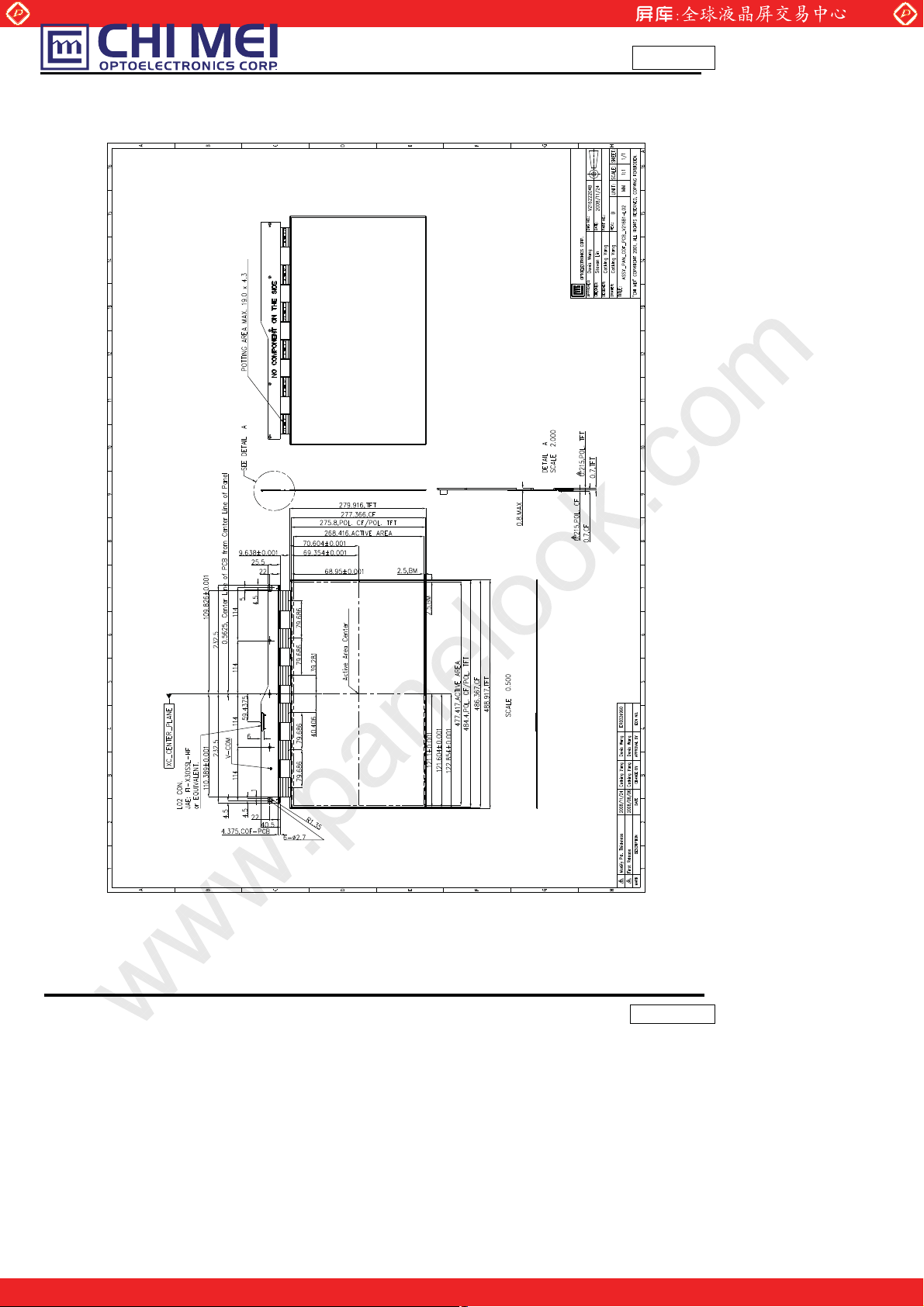
11. MECHANICAL DRAWING
-------------------------------------------------------
-------------------------------------------------------
-------------------------------------------------------
-------------------------------------------------------
-------------------------------------------------------
-------------------------------------------------------
-------------------------------------------------------
-------------------------------------------------------
----------------------------------------------
-------------------------------------------------------
-------------------------------------------------------
-------------------------------------------------------
3
4
5
6
8
12
15
19
20
22
23
9
2
Versio n 2.0
One step solution for LCD / PDP / OLED panel application: Datasheet, inventory and accessory!
www.panelook.com
Page 3
Global LCD Panel Exchange Center
3
www.panelook.com
Issued Date: Feb. 9th, 2009
Model No.: V216B1 – P02
Approval
Ver sion
Ver 2.0
Date
Feb. 9th, ’09
Page
(New)
All
REVISION HISTORY
Section
All Ap pr ov al Sp ecif icati on was first issue d.
Description
Version 2.0
One step solution for LCD / PDP / OLED panel application: Datasheet, inventory and accessory!
www.panelook.com
Page 4
Global LCD Panel Exchange Center
4
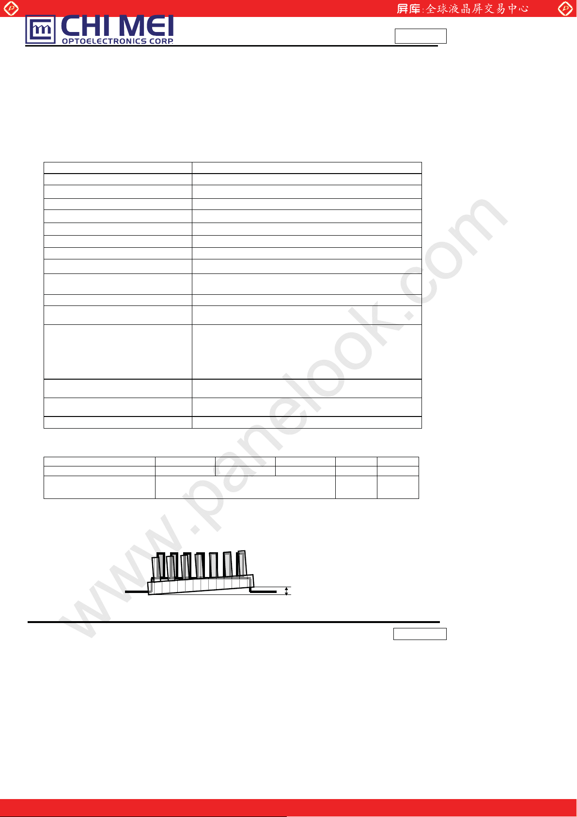
The mounting inclination of the connector makes
www.panelook.com
Issued Date: Feb. 9th, 2009
Model No.: V216B1 – P02
Approval
1. GENERAL DESCRIPTION
1.1 OVERVIEW
V216B1- P02 is a 21.6-inch wide TFT LCD cell with driver ICs and a 30- pin 1-ch LVDS interf ace. The
product supports 1366 x 768 (16.9 wide screen) mode and displays up to 16.7 ( 6-bit+Hi-FRC colors) millions
colors. The backlight unit is not built in.
1.2 CHARACTERISTICS
CHARACTERISTICS ITEMS SPECIFICATIONS
Screen D iagonal [in] 21.6
Pixels [lin es] 1366 x R.G.B. x 768
Active Area [mm] 477.417 (H) x 268.416 (V) (21.6” diagonal)
Sub -Pix el Pitch [mm] 0.1165 (H) x 0.3495 (V)
Pixel Arrangement RGB vertical stripe
Weight [g] TYP. 606
Physical Size [mm] 488.917(W) x 279.916(H) x 2.0(D) Typ.
Display Mode TN / Normally White
Contrast Ratio 800:1 Typ.
Glass thickness (Array/CF) [mm] 0.7 / 0.7
Viewing Angle (CR>10) +85/-85(H),+80/-80(V) Typ.
Color Chromaticity R=(0.644, 0.331)
Cell Trans parency [и] 7.38%Typ.s
Polarizer (CF side) Anti-glare coating,
Polarizer (TFT side) 484.4(H) x 275.8(w)
1.3 MECHANICAL SPECIFICATIONS
Weight 595 g
I/F connector mounting
position
Note (1) Please refer to the attached drawings for more information of front and back outline dimensions.
Item Min. Typ. Max. Unit Note
the screen center within ±0.5mm as the horizontal.
(2) Connector mounting position
(Typical value measured at CMO’s module: V216B1-L01)
(Typical value measured at CMO’s module: V216B1-L01)
G=(0.273,0.588)
B=(0.151,0.061)
W=(0.285,0.293)
*Pleas e refer to “color chromaticity” on p.15
(Typical value measured at CMO’s module: V216B1-L01)
(Typical value measured at CMO’s module: V216B1-L01)
484.4(H) x 275.8(w). Hardness: 3H
(2)
+/- 0.5mm
Version 2.0
One step solution for LCD / PDP / OLED panel application: Datasheet, inventory and accessory!
www.panelook.com
Page 5
Global LCD Panel Exchange Center
5
www.panelook.com
Issued Date: Feb. 9th, 2009
Model No.: V216B1 – P02
Approval
2. ABSOLUTE MAXIMUM RATINGS
2.1 ABSOLUTE RATINGS OF ENVIRONMENT (BASED ON CMO MODULE V216B1-L01)
Item Symbol
Storage Temperature TST -20 +60 ºC (1), (3)
Operating A mbient Temper ature TOP 0 +50 ºC (1), (2), (3)
Altitude Operating A OP 0 5000 M (3)
Altitu de Stor age A ST 0 12000 M (3)
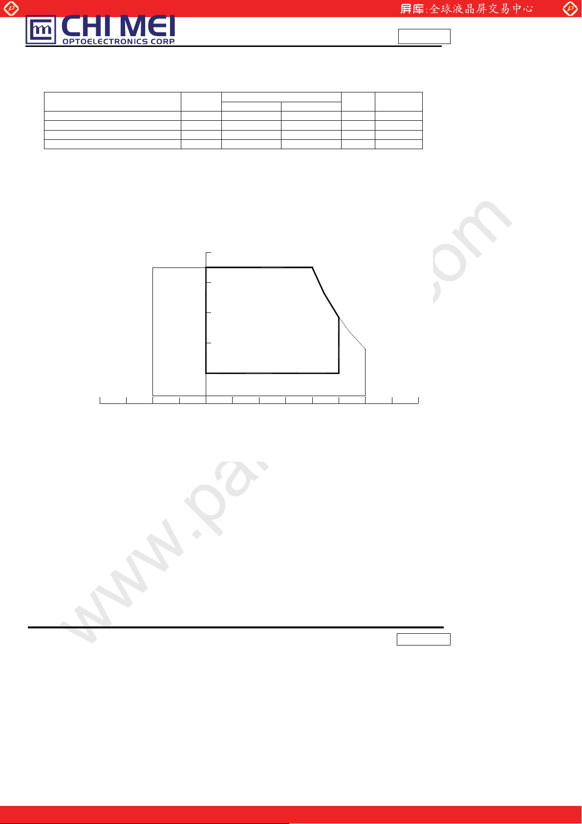
Note (1) Temperature and relative humidity range is shown in th e figure below.
(a) 90 %RH Max. (Ta Љ 40 ºC).
(b) Wet-bulb temperature should be 39 ºC Max. (Ta > 40 ºC).
(c) No condensation..
Note (2) The maximum operating temperature is based on the test condition that the surface temperature of
display area is less than or equal to 65 ºC with LCD module alone in a temperature contr oll ed
chamber. Thermal management should be considered in your product design to prevent the surface
temperature of display area from being over 65 ºC. The ran ge of operating temperature may
degrade in case of improper thermal management in your product design.
Note (3) The rating of environment is base on LCD module. Leave LCD cell alone, this environment condition can’t
be guaranteed. Except LCD cell, the customer has to consider the ability of other parts of LCD module
and LCD modu le process.
Relative Humidity (%RH)
100
90
80
60
Operating Range
40
20
Storage Range
10
Temperature (ºC)
Value
Min. Max.
Unit Note
80 60 -20 40 0 20 -40
Version 2.0
One step solution for LCD / PDP / OLED panel application: Datasheet, inventory and accessory!
www.panelook.com
Page 6

Global LCD Panel Exchange Center
6
www.panelook.com
Issued Date: Feb. 9th, 2009
Model No.: V216B1 – P02
2.2 ABSOLUTE RATINGS OF ENVIRONMENT (OPEN CELL)
Storage Condition : W ith shipping package.
Storage temperature range : 25±5 к
Storage humidity range : 50±10%RH
Shelf life : a month
2.3 ELECTRICAL ABSOLUTE RATINGS
2.3.1 ELECTRICAL ABSOLUTE RATINGS (OPEN CELL)
Item Symbol
Power Supply Voltage Vcc -0.3 6.0 V
Input Sign al Voltage VIN -0.3 3.6 V
Value
Min. Max.
Unit Note
3. ELECTRICAL CHARACTERISTICS
3.1 TFT LCD OPEN CELL
Parameter Symbol
Power Supply Voltage VCC 4.5 5.0 5.5 V (1)
Power Supply Ripple Voltage VRP - - 150 mV
Rush Current I
Power Supply Current
Differential Input High
LVD S
Interface
interface
Note (1) The modu le should be always operated within above ranges.
Note (2) Measurement Conditions:
Threshold Voltage
Differential Input Lo w
Threshold Voltage
Common Input Voltage V
Terminating Resistor R
Input High Threshold Voltage VIH 2.7 - 3.3 V CMOS
Input Low Threshold Voltage VIL 0 - 0.7 V
White - 0.50 - A
Black - 0.85 0.95 A
Vertical Stripe
Ta = 25 ± 2 ºC
Min. Typ. Max.
- - 3.0 A (2)
RUSH
ICC
+100 - - mV
V
LVT H
- - -100 mV
V
LVTL
1.125 1.25 1.375 V
LVC
- 100 - ohm
T
- 0.75 - A
Value
Unit Note
Approval
(3)
Version 2.0
One step solution for LCD / PDP / OLED panel application: Datasheet, inventory and accessory!
www.panelook.com
Page 7
Global LCD Panel Exchange Center
7
www.panelook.com
Issued Date: Feb. 9th, 2009
Model No.: V216B1 – P02
Approval
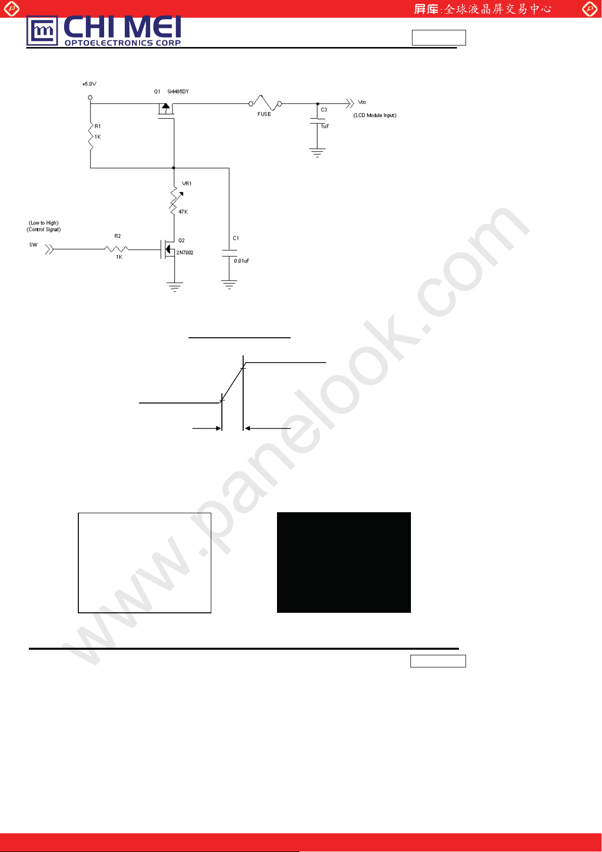
Vcc rising time is 470us
+5V
0.9Vcc
0.1Vcc
GND
470us
Note (3) The specified power supply current is under the conditions at Vcc = 5 V, Ta = 25 ± 2 ºC, fv = 60 Hz,
whereas a power dissipation check pattern below is dis played.
a. White Pattern
Active Area
b. Black Pattern
Active Area
Version 2.0
One step solution for LCD / PDP / OLED panel application: Datasheet, inventory and accessory!
www.panelook.com
Page 8
Global LCD Panel Exchange Center
8
R
SCAN DRIVER IC
GND
www.panelook.com
Issued Date: Feb. 9th, 2009
Model No.: V216B1 – P02
Approval
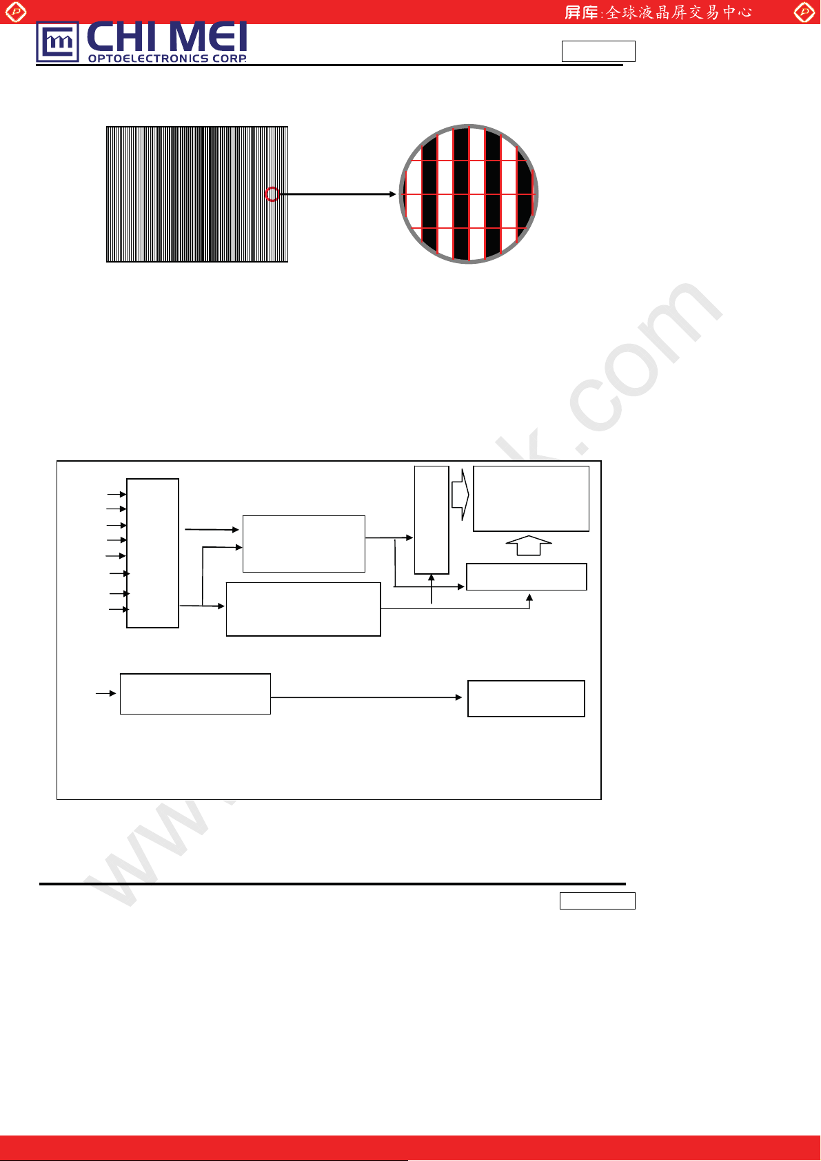
c. Vertical Stripe Pattern
4. BLOCK DIAGRAM
4.1 TFT LCD OPEN CELL
RX0(+/-)
RX1(+/-)
RX2(+/-)
RX3(+/-)
RXCLK(+/-)
SELLVDS
Vcc
(JAE: FI-X30SSL-HF)
INPUT CONNECTOR
V/L
Inverter (W/O)
Active Area
TIMING
CONTROLLER
DC/DC CONVERTER &
REFERENCE VOLTAGE
R
R
B
R
B
R
R
G
B
R
G
B
R
G
B
G
B
DATA DRIVER IC
BACKLIGHT UNIT
G
B
G
B
R
G
B
R
G
B
TFT LCD PANEL
(1366x3x768)
Version 2.0
One step solution for LCD / PDP / OLED panel application: Datasheet, inventory and accessory!
www.panelook.com
Page 9
Global LCD Panel Exchange Center
9
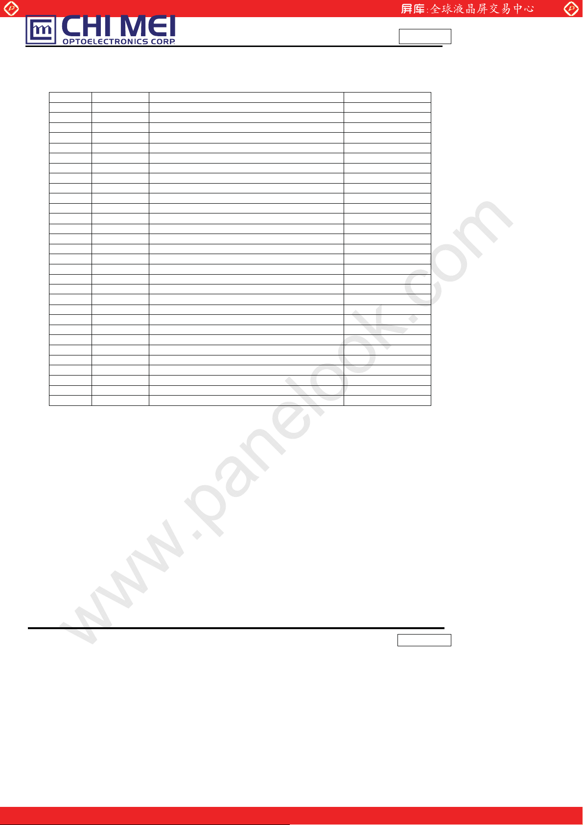
Pin No.
Symbol
Description
Note
1 NC No Conn ection
(2)
2 NC No Conn ection
(2)
3 NC No Conn ection
(2)
4 GND Ground
12 RX2+
Positive tr ansmission data of pixel 2
13 GND Ground
21 SELLVDS
S elect LVDS data format
(3)
22 NC No Conn ection
(2)
23 GND Ground
24 GND Ground
25 GND Ground
5. INPUT TERMINAL PIN ASSIGNMENT
5.1 TFT LCD MODULE
5 RX0- Negative transmission data of pixel 0
6 RX0+ Positiv e transmission data of pixel 0
7 GND Ground
8 RX1- Negative transmission data of pixel 1
9 RX1+ Positiv e transmission data of pixel 1
10 GND Ground
11 RX2- Negativ e transmission data of pixel 2
14 RXCLK- Negative of clock
15 RXCLK+ Positive of clock
16 GND Ground
17 RX3- Negative tr ansmission data of pixel 3
18 RX3+ Positive transmission data of pixel 3
19 GND Ground
20 NC No Conn ection (2)
www.panelook.com
Issued Date: Feb. 9th, 2009
Model No.: V216B1 – P02
Approval
26 VCC Power supply: +5V
27 VCC Power supply: +5V
28 VCC Power supply: +5V
29 VCC Power supply: +5V
30 VCC Power supply: +5V
Note (1) Connector part no.: JAE: FI-X30SSL-HF (LCDS) or compatible
Note (2) Reserved for CMO internal use, please leave it open
Note (3) Low: JEIDA data format. High/open: VESA data format.
Note (4) Logic level voltage definition: Low: 0V, High: 3.3V
Version 2.0
One step solution for LCD / PDP / OLED panel application: Datasheet, inventory and accessory!
www.panelook.com
Page 10
Global LCD Panel Exchange Center
10
ܔೈ
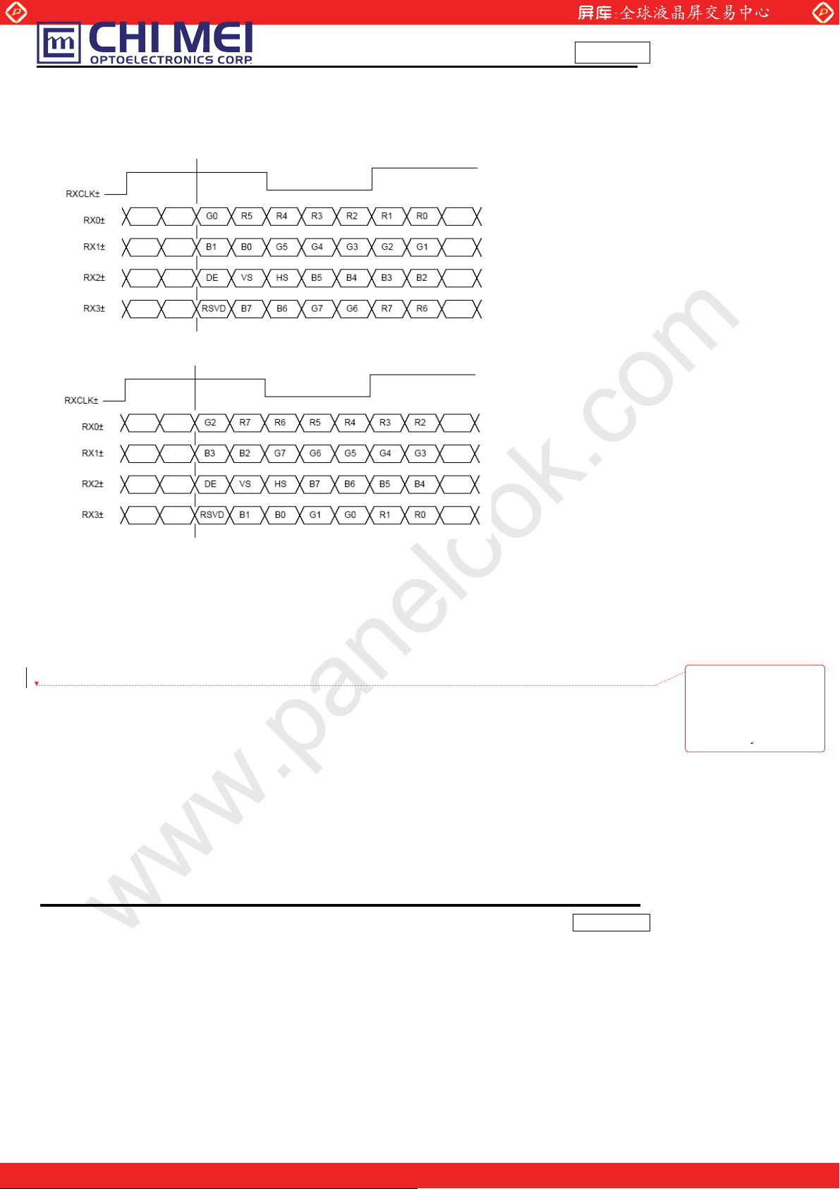
5.2 LV D S DATA MAPPIN G TABL E
SELLVDS = H or Open (VESA)
SELLVDS = L (JEIDA)
www.panelook.com
Issued Date: Feb. 9th, 2009
Model No.: V216B1 – P02
Approval
R0~R7: Pixel R Data (7; MSB, 0; LSB)
G0~G7: Pixel G Data (7; MSB, 0; LSB)
B0~B7: Pixel B Data (7; MSB, 0; LSB)
DE : Data enable signal
Notes( 1) RSVD(reserved)pins on the transmitter shall be “H” or “L”
: Note (2) Specified
values are for l amp (Refer
to 3.2 for further
information).
Version 2.0
One step solution for LCD / PDP / OLED panel application: Datasheet, inventory and accessory!
www.panelook.com
Page 11
Global LCD Panel Exchange Center
11
www.panelook.com
Issued Date: Feb. 9th, 2009
Model No.: V216B1 – P02
Approval
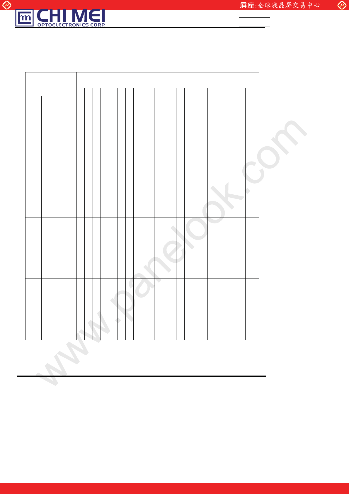
5.3 COLOR DATA INPUT ASSIGNMENT
The brightness of each primary color (red, green and blue) is based on the 8-bit gray scale data in put f or the
color. The higher the binary input, the brighter the color. The table below provides the assignment of color
versus data input.
Color
R7 R6 R5 R4 R3 R2 R1 R0 G7 G6 G5 G4 G3 G2 G1 G0 B7 B6 B5 B4 B3 B2 B1 B0
Black
Red
Green
Blue
Basic
Cyan
Colors
Magenta
Yellow
White
Red(0) / Dark
Red(1)
Red(2)
Gray
Scale
Of
Red
Gray
Scale
Of
Green
Gray
Scale
Of
Blue
Note (1) 0: Low Level Voltage, 1: High Level Voltage
:
:
Red(253)
Red(254)
Red(255)
Green(0) / Dark
Green(1)
Green(2)
:
:
Green(253)
Green(254)
Green(255)
Blue(0) / Dark
Blue(1)
Blue(2)
:
:
Blue(253)
Blue(254)
Blue(255)
0
0
0
1
1
1
0
0
0
0
0
0
0
0
0
1
1
1
1
1
1
1
1
1
0
0
0
0
0
0
0
0
0
:
:
:
:
:
:
1
1
1
1
1
1
1
1
1
0
0
0
0
0
0
0
0
0
:
:
:
:
:
:
0
0
0
0
0
0
0
0
0
0
0
0
0
0
0
0
0
0
:
:
:
:
:
:
0
0
0
0
0
0
0
0
0
Data Signal
Red Green Blue
0
0
0
0
0
0
0
0
0
0
0
0
0
0
0
0
0
1
1
1
1
1
0
0
0
0
0
0
0
0
0
0
0
0
0
0
0
0
0
1
1
1
1
1
1
1
1
0
0
0
0
0
0
0
0
0
0
0
0
0
0
0
0
0
1
1
1
1
0
0
0
0
0
1
1
1
1
1
1
1
1
1
1
1
1
1
1
1
1
1
0
0
0
0
0
0
0
0
1
1
1
1
1
1
1
1
1
1
1
1
1
1
1
1
1
0
0
0
0
1
1
1
1
1
1
1
1
1
1
1
1
1
1
1
1
1
0
0
0
0
0
0
0
0
0
0
0
0
0
0
0
0
0
0
0
0
0
1
0
0
0
0
0
0
0
0
0
0
0
0
0
0
0
1
0
0
0
0
0
0
0
0
0
0
0
0
0
:
:
:
:
:
:
:
:
:
:
:
:
:
:
:
:
:
:
:
:
:
:
:
:
:
:
:
:
:
:
:
:
:
:
1
1
1
0
1
0
0
0
0
0
0
0
0
0
0
0
0
1
1
1
1
0
0
0
0
0
0
0
0
0
0
0
0
0
1
1
1
1
1
0
0
0
0
0
0
0
0
0
0
0
0
0
0
0
0
0
0
0
0
0
0
0
0
0
0
0
0
0
0
0
0
0
0
0
0
0
0
0
0
0
1
0
0
0
0
0
0
0
0
0
0
0
0
0
0
0
1
0
0
0
0
0
:
:
:
:
:
:
:
:
:
:
:
:
:
:
:
:
:
:
:
:
:
:
:
:
:
:
:
:
:
:
:
:
:
:
0
0
0
0
0
1
1
1
1
1
1
0
1
0
0
0
0
0
0
0
0
0
1
1
1
1
1
1
1
0
0
0
0
0
0
0
0
0
0
1
1
1
1
1
1
1
1
0
0
0
0
0
0
0
0
0
0
0
0
0
0
0
0
0
0
0
0
0
0
0
0
0
0
0
0
0
0
0
0
0
0
0
0
0
0
0
0
0
0
0
0
0
0
0
0
0
0
0
0
0
0
0
:
:
:
:
:
:
:
:
:
:
:
:
:
:
:
:
:
:
:
:
:
:
:
:
:
:
:
:
:
:
:
:
:
:
0
0
0
0
0
0
0
0
0
0
0
0
0
1
1
1
1
0
0
0
0
0
0
0
0
0
0
0
0
0
1
1
1
1
0
0
0
0
0
0
0
0
0
0
0
0
0
1
1
1
1
0
0
0
0
0
0
0
0
0
0
0
0
1
1
1
1
1
1
1
1
1
1
1
1
0
0
0
0
1
1
1
1
0
0
0
0
0
0
0
0
0
0
0
0
:
:
:
:
:
:
:
:
0
0
0
0
0
0
0
0
0
0
0
0
0
0
0
0
0
0
0
0
0
0
0
0
:
:
:
:
:
:
:
:
0
0
0
0
0
0
0
0
0
0
0
0
0
0
0
0
0
0
0
1
0
0
1
0
:
:
:
:
:
:
:
:
1
1
0
1
1
1
1
0
1
1
1
1
Version 2.0
One step solution for LCD / PDP / OLED panel application: Datasheet, inventory and accessory!
www.panelook.com
Page 12
Global LCD Panel Exchange Center
12
Signal
Item Symbol
Min. Typ. Max. Unit Note
Frequency
1/Tc 60 76 82 MHZ
Input cycle to
www.panelook.com
Issued Date: Feb. 9th, 2009
Model No.: V216B1 – P02
Approval
6. INTERFACE TIMING
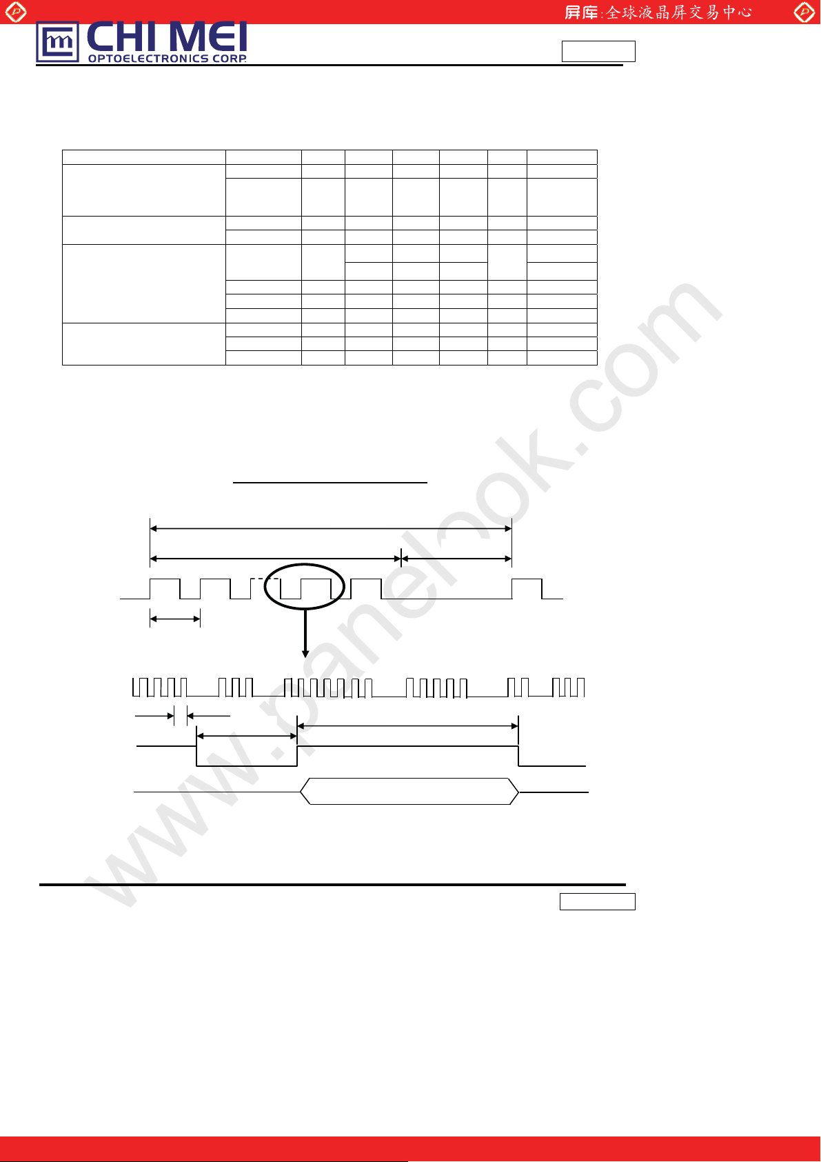
6.1 INPUT SIGNAL TIMING SPECIFICATIONS
The input signal timing specifications are shown as the following table and timin g diagram.
LVDS Receiver Clock
cycle Jitter
LVDS Receiver Data
Vertical Active Display Term
Note (1) Since this module is operated in DE only mode, Hsync and Vsync input signals should be set to low
logic level. Otherwise, this module would operate abnormally.
(2) Please refer to 5.1 for detail information.
Setup Time Tlvsu 600 - - ps
Hold Time Tlvhd
Frame Rate
Total Tv 778 806 888 Th Tv=Tvd+Tvb
Display Tvd 768 768 768 Th Blank Tvb 10 38 120 Th Total Th 1442 1560 1936 Tc Th=Thd+T hb
Display Thd 1366 1366 1366 Tc - Horizontal Active Display Term
Blank Thb 76 194 570 Tc -
Trcl
Fr
-
600 - - ps
47 50 53
57 60 63
200 ps
-
Hz
INPUT S IGNAL TIMING DIAGRAM
DE
Th
DCLK
DE
DATA
Tvd
Tv
Tvb
Thd
Valid display data (1366 clocks)
Version 2.0
One step solution for LCD / PDP / OLED panel application: Datasheet, inventory and accessory!
www.panelook.com
Page 13
Global LCD Panel Exchange Center
13
14
14
14
14
14
14
14
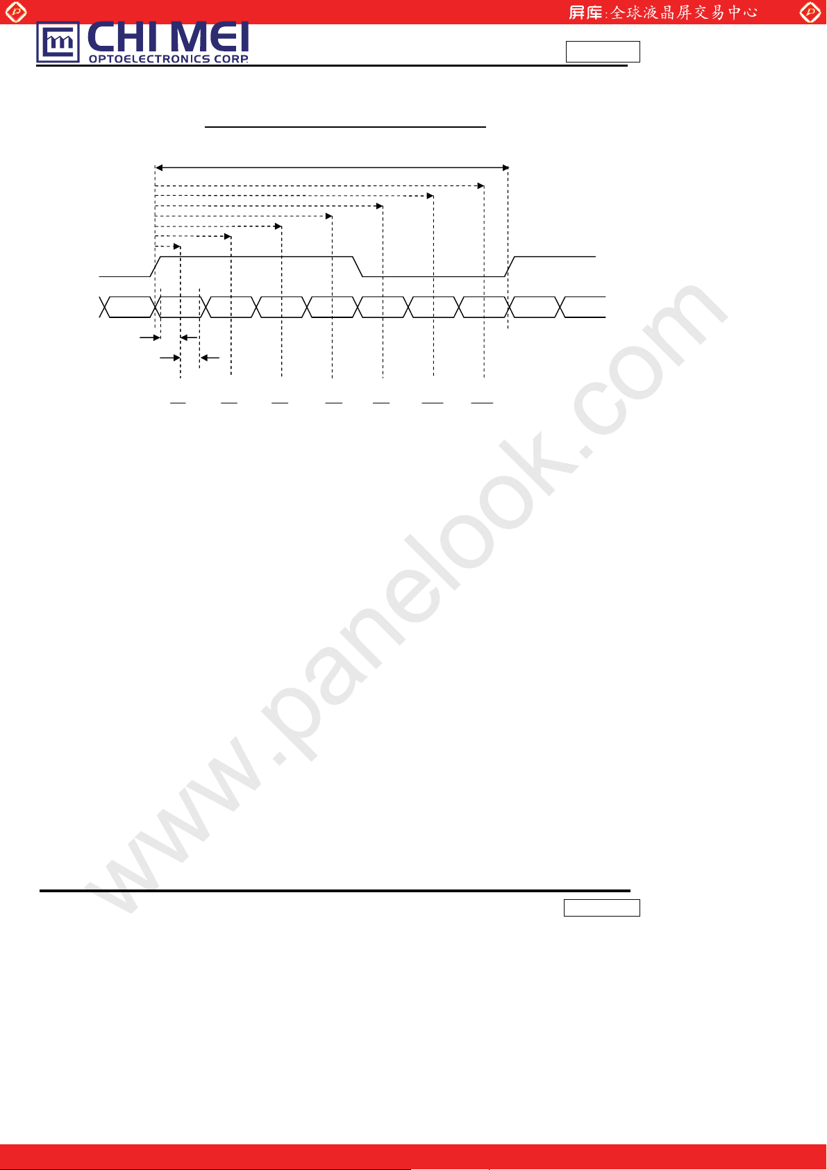
LVDS RECEIVER INTERFACE TIMING DIAGRAM
RXCLK+/-
RXn+/-
Tlvsu
Tlvhd
1T
3T
5T
www.panelook.com
Tc
7T
9T
11T
Issued Date: Feb. 9th, 2009
Model No.: V216B1 – P02
Approval
13T
Version 2.0
One step solution for LCD / PDP / OLED panel application: Datasheet, inventory and accessory!
www.panelook.com
Page 14
Global LCD Panel Exchange Center
14
Љ
Љ
Љ
Љ
Љ
Љ
Љ
100ms
Љ
T
Option
Signals
Љ
Љ
Љ
www.panelook.com
Issued Date: Feb. 9th, 2009
Model No.: V216B1 – P02
Approval
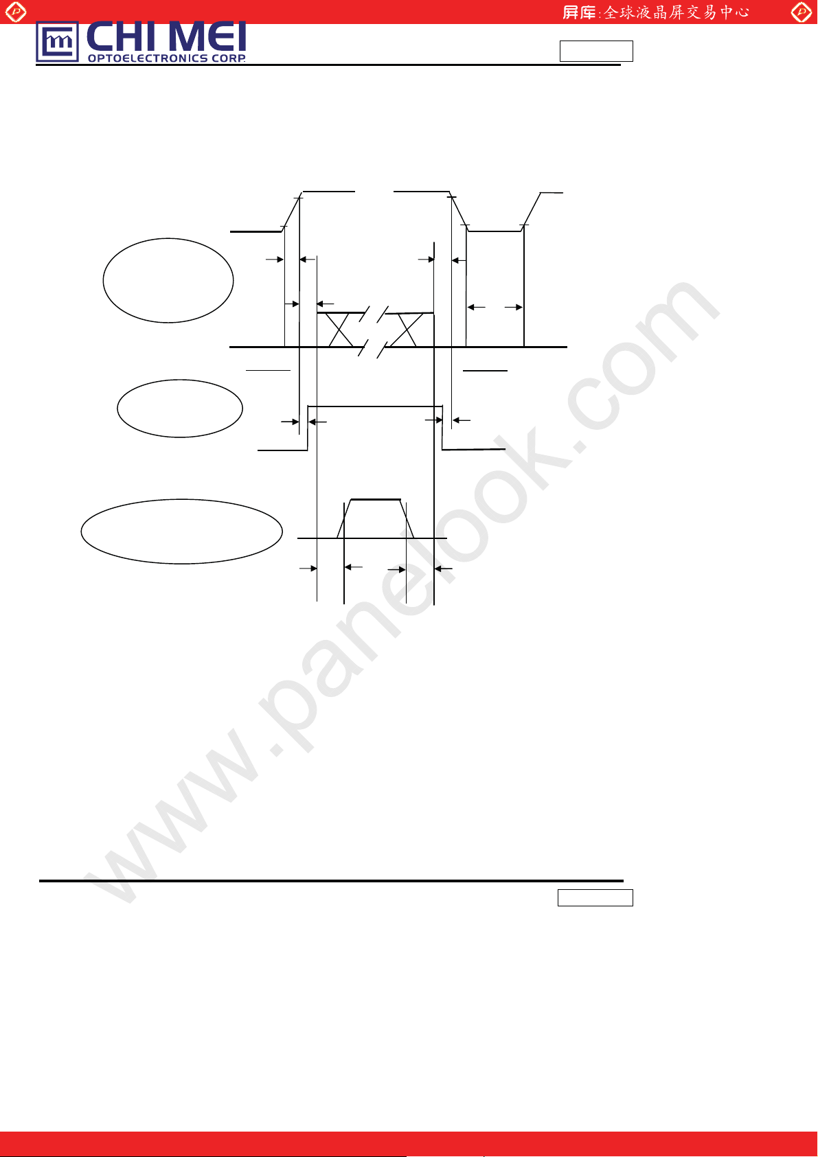
6.2 POWER ON/OFF SEQUENCE
To prevent a latch-up or DC operation of LCD module, the power on/off sequence should be as the
diagram below.
T4
0V
10ms
50ms
50ms
0.5ЉT
0
0
1s
1
T
2
T
3
LVD S S i gnals
0V
CC
0.1V
Power On
2
T
VALI D
T
3
T1
0.1V
T4
Power Off
cc
0ЉT
7
T2
0
T
8
T3
T7
T
8
(SELLVDS)
50%
Backlight (Recommended)
500ms
T5
6
T
5
50%
T
6
Note (1) The supply voltage of the external system for the module input should follow the definition of Vcc.
Note (2) Apply the lamp voltage within the LCD operation range. When the backlight turns on before the LCD
operation or the LCD turns off bef ore the backlight turn s off, the display may momentarily become
abnormal screen.
Note (3) In case of Vcc is in off level, please keep the level of i nput signals on the low or high impedance. If
T2<0,that maybe cause electrical overstress failure.
Note (4) T4 should be measured after the module has been fully discharged between power off and on period.
Note (5) Interface signal shall not be kept at high impedance when the power is on.
Power ON/OFF Sequence
Version 2.0
One step solution for LCD / PDP / OLED panel application: Datasheet, inventory and accessory!
www.panelook.com
Page 15
Global LCD Panel Exchange Center
15
www.panelook.com
Issued Date: Feb. 9th, 2009
Model No.: V216B1 – P02
Approval
7. OPTICAL CHARACTERISTICS
7.1 TEST CONDITIONS
Item Symbol Value Unit
Ambient Temperature Ta 25Ć2
Ambient Humidity Ha 50Ć10 %RH
Supply Voltage VCC 5.0 V
Input Signal According to typical value in "3. ELECTRICAL CHARACTERISTICS”
Inverter Current IL 7.0 mA
Inverter Driving Frequency FL 50 KHz
Dimming Frequency FB 160 (type) Hz
Minimum Duty Ratio D
Maximum Duty R atio D
Inverter Ampower (27-D024817)
o
C
20 %
MIN
100 %
MAX
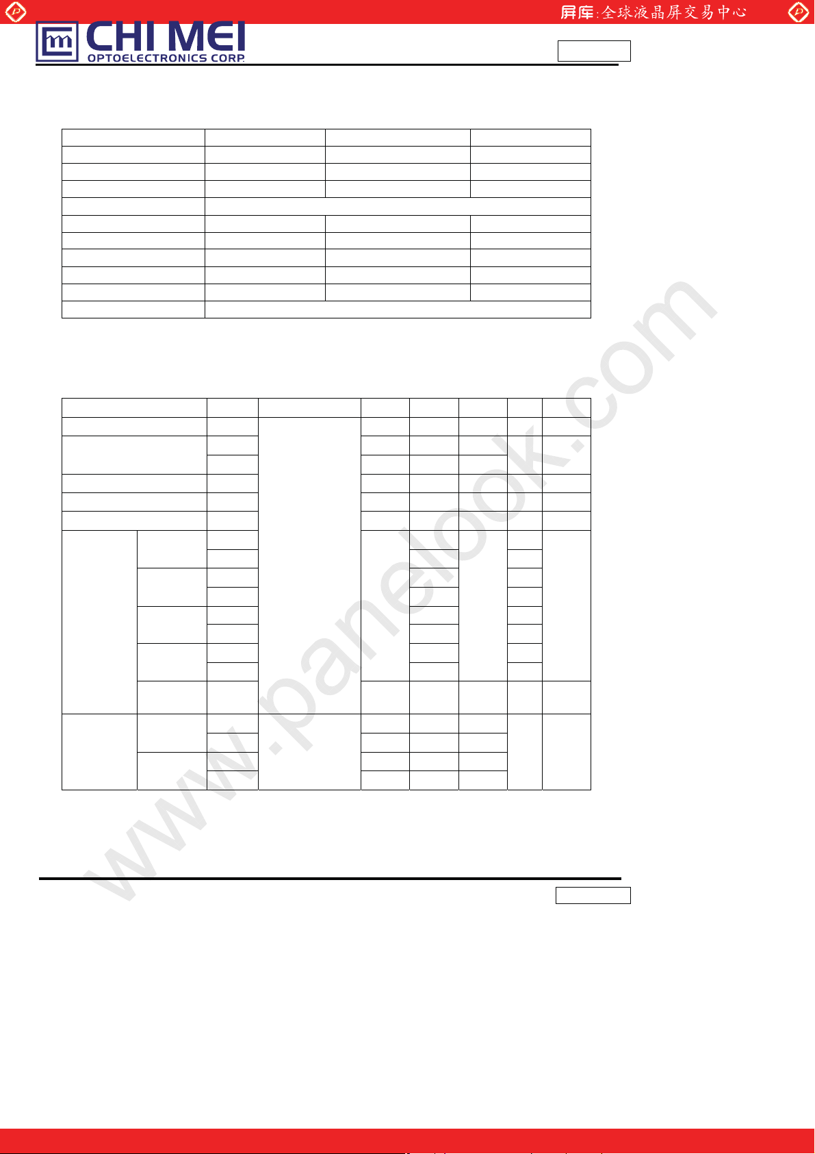
7.2 OPTICAL SPECIFICATIONS
The relativ e measurement methods of optical characteristics are shown as below. The following items should
be measured under the test conditions described in 7.1 and stable environment shown in Note (5).
Item Symbol
Contrast Ratio CR 600 800 - (2)
Response Ti me
Center Luminanc e of White L
White Variation
Cross Talk CT 4 % (5)
Red
Green
Color
Chromaticity
Viewing
Angle
Blue
White
Color Gamut
Horizontal
Vertic al
TR 1.3 2.2
T
3.7 5.8
F
C
δW
Rx 0.644 -
Ry 0.331 -
Gx 0.273 -
Gy 0.588 -
Bx 0.151 -
By 0.061 -
Wx 0.285 -
Wy
CG
θx+
θ
-
x
θY+
-
θ
Y
Condition Min. Typ. Max. Unit Note
ms
300 400 (4)
1.3 - (7)
θ
=0°, θY =0°
x
Viewing Angle at
Normal Direction
With CMO’s
module:
V216B1-L01
CR≥10
With CMO’s
module:
V216B1-L01
Typ.
-0.03
0.293
68 72 %
75 85
75 85
70 80
70 80
Typ.
+0.03
-
Deg.
(3)
(0),(6)
NTSC
Ratio
(1)
Version 2.0
One step solution for LCD / PDP / OLED panel application: Datasheet, inventory and accessory!
www.panelook.com
Page 16
Global LCD Panel Exchange Center
16
T
ime
www.panelook.com
Issued Date: Feb. 9th, 2009
Model No.: V216B1 – P02
Note (0) Light source is the standard light source ”C” which is defined by CIE and driving voltage are based on
suitable gamma voltages. The calculating method is as following :
1. M easur e Module’s and BLU’s spectrum. White is without signal input and R,G,B are with signal input.
BLU (for V216B1-L01) is supplied by CMO.
2. Calcul ate c ell’s spectru m.
Calculate cell’s chromaticity by using the spectrum of standard light source “C”.
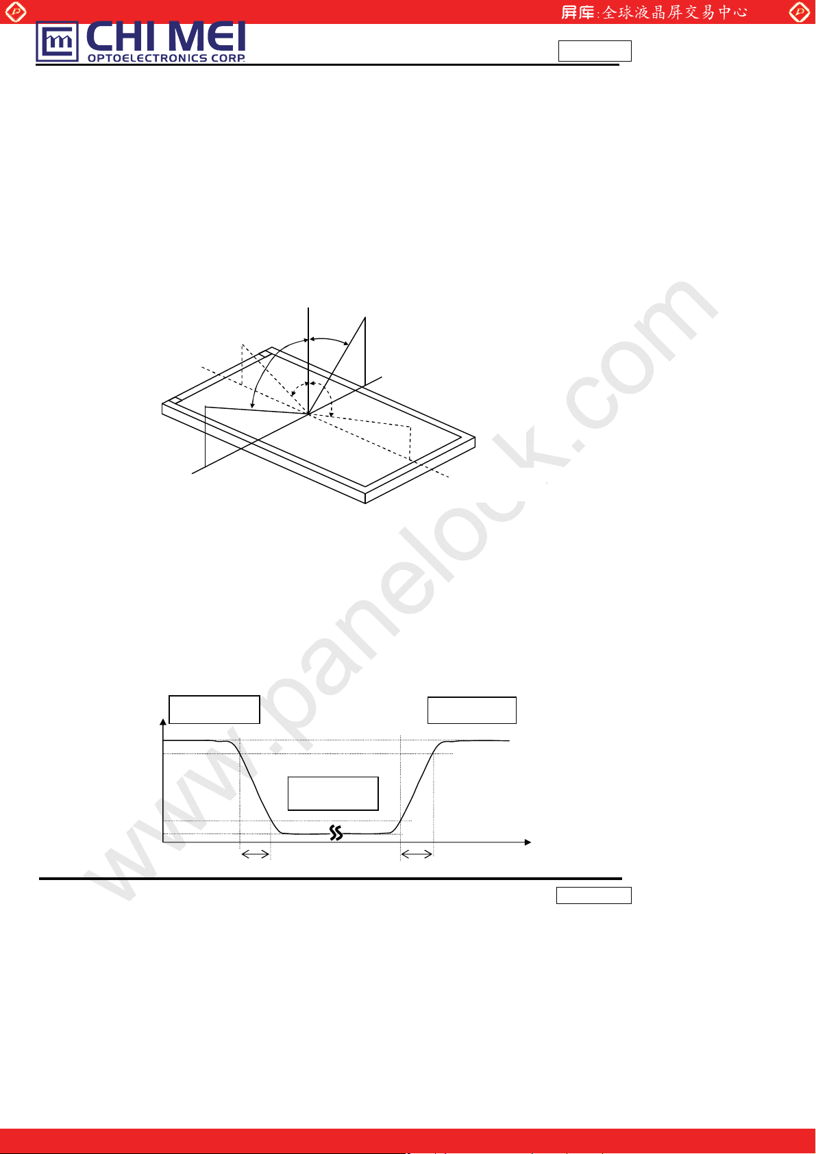
Note (1) Definition of Viewing Angle (θx, θy):
Viewing angles ar e measured by EZ -Contras t 160R (Eldim)
Normal
θx = θy = 0º
θX- = 90º
x-
θy- θy+
θx−
θx+
12 o’clock direction
y+
y+
= 90º
θ
6 o’clock
y-
= 90º
θ
y-
x+
θX+ = 90º
Note (2) Definition of Contrast Ratio (CR):
The contrast r atio can be calculated by the following expression.
Contrast Ratio (CR) = L255 / L0
L255: Luminance of gray level 255
L 0: Lumin ance of gr ay level 0
CR = CR (5),
CR (X) is corresponding to the Contrast Ratio of the point X at the figure in Note (7).
Note (3) Definition of Response Time (T
, TF):
R
Gray Level 255
Gray Level 255
Optical
100%
90%
10%
0%
TR
Gray L evel 0
TF
Response
Approval
Version 2.0
One step solution for LCD / PDP / OLED panel application: Datasheet, inventory and accessory!
www.panelook.com
Page 17
Global LCD Panel Exchange Center
17
Active Area
(0, 0 )
(D,W )
Gray 0
Active Area
(D,W)
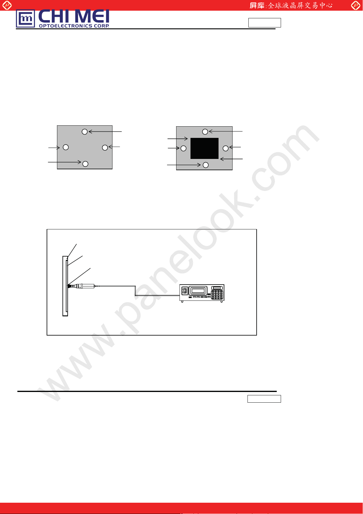
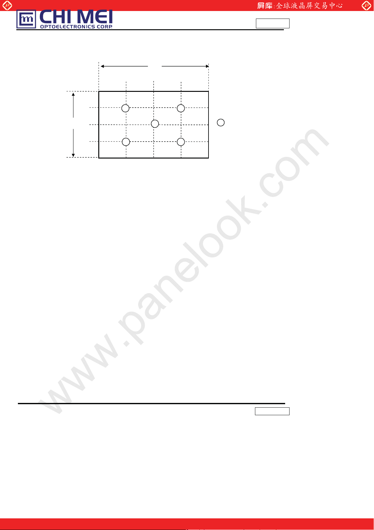
Note (4) Def inition of Lu minance of White (LC):
Measure th e lu minance of gray level 255 at center point and 5 points
LC = L (5)
L (X) is corresponding to the luminance of the point X at the figur e in Note (7).
Note (5) Definition of Cross Talk (CT):
CT = | Y
Where:
(0, 0)
Y
(D/8,W/2)
A, L
Y
(D/2,7W/8)
A, D
Note (6) Measurement Setup:
The LCD module should be stabilized at giv en temperature for 1 hour to avoid abrupt temperature
change during measuring. In order to stabilize the luminance, the measurement should be executed
after lighting Backlight for 1 hour in a windless room.
Note (7) Definition of White Variation ( δW):
Measure th e lu minance of gray level 255 at 5 points
δW = Maximum [L (1), L (2), L (3), L (4), L (5)] / Minimum [L (1), L (2), L (3), L (4), L (5)]
– YA | / YA × 100 (%)
B
Y
= Luminance of measured location without gray level 0 pattern (cd/m2)
A
Y
= Luminance of measured location with gray level 0 pattern (cd/m2)
B
Y
A, U
Gray 128
Y
A, R
LCD Module
LCD Panel
Center of the Screen
(D/2,W/8)
(7D/ 8,W /2 )
www.panelook.com
(D/4,W/4)
Y
(D/8,W/2)
B, L
Y
(D/2,7W/8)
B, D
Display Color Analyzer
(Minolta CA210)
Light S hield Room
(Ambient Luminance < 2 lux)
Issued Date: Feb. 9th, 2009
Model No.: V216B1 – P02
Approval
Y
(D/2,W/8)
B, U
Y
(7D/8,W/2)
B, R
(3D/4,3W/4)
Gray 128
Version 2.0
One step solution for LCD / PDP / OLED panel application: Datasheet, inventory and accessory!
www.panelook.com
Page 18
Global LCD Panel Exchange Center
18
W
Vertical Line
W/4
W/2
3W /4
D/4 D/ 2 3D/4
www.panelook.com
Issued Date: Feb. 9th, 2009
Horizontal Line
D
1 2
X
5
3 4
Active Area
: Test Point
X=1 to 5
Model No.: V216B1 – P02
Approval
Version 2.0
One step solution for LCD / PDP / OLED panel application: Datasheet, inventory and accessory!
www.panelook.com
Page 19
Global LCD Panel Exchange Center
19
www.panelook.com
Issued Date: Feb. 9th, 2009
Model No.: V216B1 – P02
8. DEFINITION OF LABELS
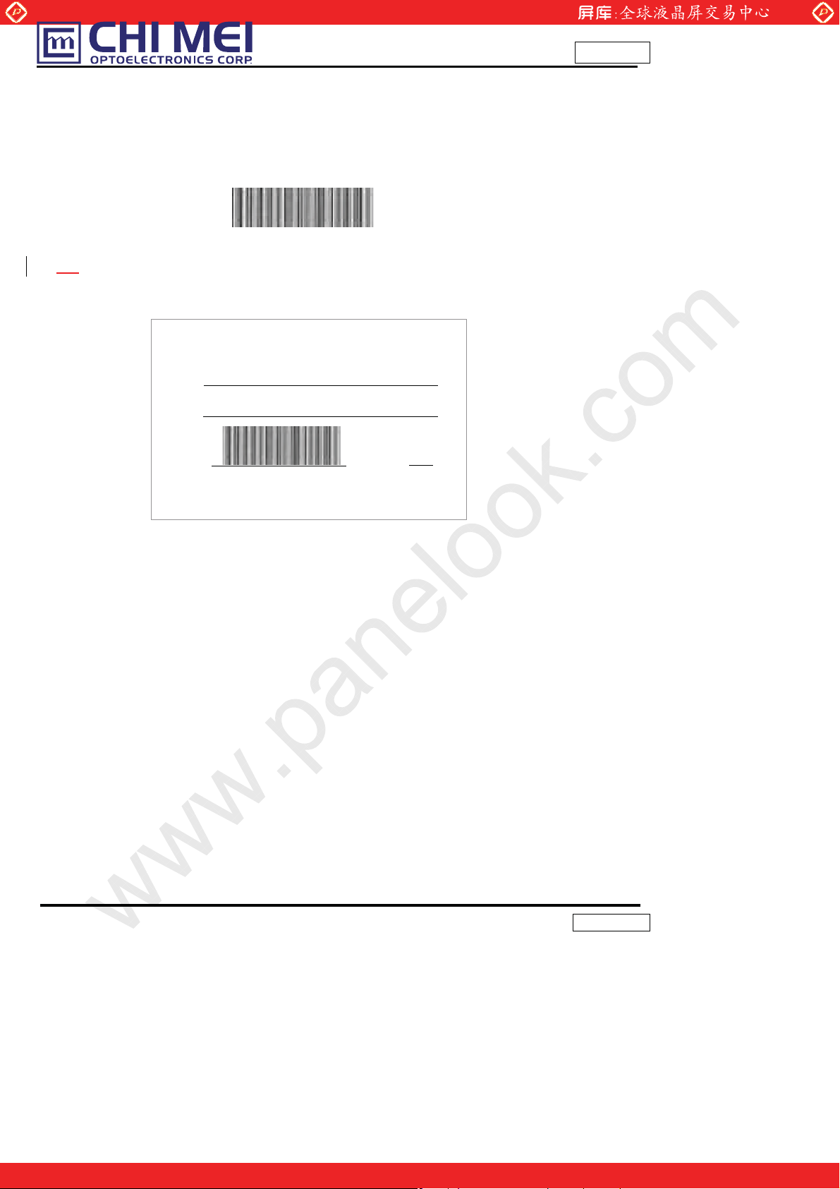
8.1 OPEN CELL LABEL
The barcode nameplate is pasted on each open cell as illustration for CMO internal control.
XXXXXXXXXXXX
8.2 CARTON LABEL
The barcode nameplate is pasted on each box as illustration, and its definitions are as followin g explanation
P.O. NO.
Parts ID.
Carton ID.
XXXXXXXXXXXXXX
Quantities 27
Made in XXXX
(a) Model Name: V216B1-P04
(b) Carton ID: CMO internal control
(c) Quantities: 27
(d) Produc tion Location:XX XX, f or exampl e:TAIWAN or CHINA .
Approval
Version 2.0
One step solution for LCD / PDP / OLED panel application: Datasheet, inventory and accessory!
www.panelook.com
Page 20
Global LCD Panel Exchange Center
20
9. packaging
9.1 packing specifications
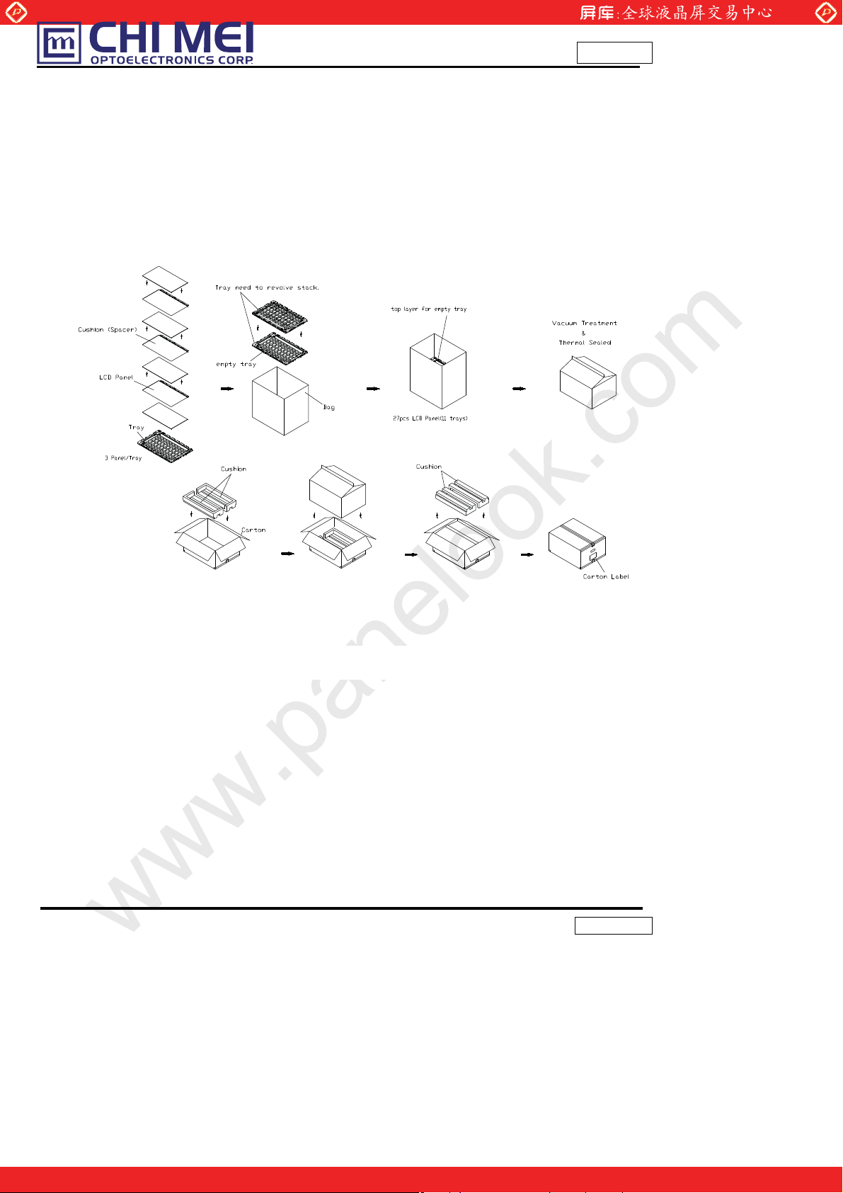
(1) 27 LCD TV Panels / 1 Box
(2) Box dimensions : 640(L) x 490(W) x 320(H) mm
(3) Weight : Approx.24.2Kg
9.2 packing Method
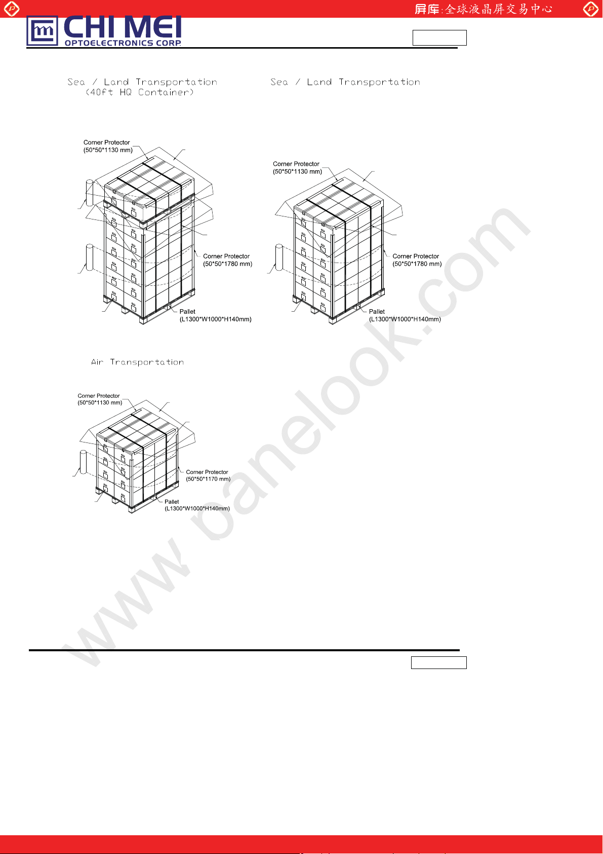
Figures 9-1 and 9-2 are the packing method
www.panelook.com
Issued Date: Feb. 9th, 2009
Model No.: V216B1 – P02
Approval
Figure.9-1 packing method
Version 2.0
One step solution for LCD / PDP / OLED panel application: Datasheet, inventory and accessory!
www.panelook.com
Page 21
Global LCD Panel Exchange Center
21
PE Sheet
Film
www.panelook.com
Issued Date: Feb. 9th, 2009
Model No.: V216B1 – P02
Approval
PE Sheet
Film
Carton La bel
PP Belt
Film
Carton La bel
PP Belt
PE Sheet
PP Bel t
Film
Carton Label
Figure.9-2 packing method
Version 2.0
One step solution for LCD / PDP / OLED panel application: Datasheet, inventory and accessory!
www.panelook.com
Page 22
Global LCD Panel Exchange Center
22
ܔೈ
www.panelook.com
Issued Date: Feb. 9th, 2009
Model No.: V216B1 – P02
Approval
10. PRECAUTIONS
10.1 ASSEMBLY AND HANDLING PRECAUTIONS
(1) Do not apply rough force such as bending or twisting to the product during assembly.
(2) To assemble backlight or install module into user’s system can be only in clean working areas. The dust
and oil may cause electrical short or worsen the polarizer.
(3) It’s not permitted to have pressure or impulse on the module because the LCD panel will be damaged.
(4) Always follow the correct power sequence when the product is connecting and operating. This can
prevent damage to the CMOS LSI chips during latch-up.
(5) Do not pull the I/F connector in or out while the module is operating.
(6) Use a soft dry cloth without chemicals f or cleaning, because the surface of polarizer is very soft an d
easily scratched.
(7) It is dangerous that moisture come into or contacted the product, because moisture may damage the
product when it is operating.
(8) High temperatur e or humidity may reduce th e performance of module. Please store this pr oduct within
the specified storage conditions.
(9) When ambient temperature is lower than 10ºC may reduce the display quality. For example, the
response time will become slowly.
10.2 SAFETY PRECAUTIONS
(1) If the liquid crystal material leaks from the panel, it should be kept away from the eyes or mouth. In case
of contact with hands, skin or clothes, it has to be washed away thoroughly with soap.
(2) After the product’s end of life, i t is not harmful in case of normal opera tion and stor age.
: The startup voltage
of Backlight is
approximately 1000 Volts.
It may c ause electrical
shock while assembling
with inverter. Do not
disassem bl e the module or
insert anything i nto the
Backlight unit.
Version 2.0
One step solution for LCD / PDP / OLED panel application: Datasheet, inventory and accessory!
www.panelook.com
Page 23
Global LCD Panel Exchange Center
23
11. Mechanical Drawing
www.panelook.com
Issued Date: Feb. 9th, 2009
Model No.: V216B1 – P02
Approval
࡛ભሽٝڶૻֆ
Version 2.0
One step solution for LCD / PDP / OLED panel application: Datasheet, inventory and accessory!
www.panelook.com
 Loading...