

Page 1
Global LCD Panel Exchange Center
MODEL NO.: V215H1
www.panelook.com
PRODUCT SPECIFICATION
□ Tentative Specification
□ Preliminary Specification
■ Approval Specification
SUFFIX: LE1
Customer:
APPROVED BY SIGNATURE
Name / Title
Note
Please return 1 copy for your confirmation with your
signature and comments.
Approved By Checked By Prepared By
Chao-Chun Chung Roger Huang Vita Wu
Version 2.1 1 DateΚΚΚΚ22 Sept 2010
The copyright belongs to CHIMEI InnoLux. Any unauthorized use is prohibited
One step solution for LCD / PDP / OLED panel application: Datasheet, inventory and accessory!
www.panelook.com
Page 2
Global LCD Panel Exchange Center
www.panelook.com
PRODUCT SPECIFICATION
CONTENTS
1. GENERAL DESCRIPTION ............................................................................................................................................ 5
1.1 OVERVIEW ..........................................................................................................................................................5
1.2 FEATURES ..........................................................................................................................................................5
1.3 APPLICATION...................................................................................................................................................... 5
1.4 GENERAL SPECIFICATIONS .............................................................................................................................5
1.5 MECHANICAL SPECIFICATIONS....................................................................................................................... 6
2. ABSOLUTE MAXIMUM RATINGS ................................................................................................................................7
2.1 ABSOLUTE RATINGS OF ENVIRONMENT........................................................................................................7
2.2 PACKAGE STORAGE.......................................................................................................................................... 8
2.3 ELECTRICAL ABSOLUTE RATINGS .................................................................................................................. 8
2.3.1 TFT LCD MODULE ....................................................................................................................................8
3. ELECTRICAL CHARACTERISTICS .............................................................................................................................9
3.1 TFT LCD MODULE ..............................................................................................................................................9
3.2 BACKLIGHT CONNECTOR PIN CONFIGURATION......................................................................................... 11
3.2.1 LED LIGHT BAR CHARACTERISTICS ................................................................................................... 11
3.2.2 LIGHTBAR Connector Pin Assignment ...................................................................................................12
3.3 LVDS INPUT SIGNAL SPECIFICATIONS .........................................................................................................12
3.3.1 LVDS DATA MAPPING TABLE ................................................................................................................13
4. BLOCK DIAGRAM OF INTERFACE ...........................................................................................................................14
4.1 TFT LCD MODULE ............................................................................................................................................14
5. INPUT TERMINAL PIN ASSIGNMENT ....................................................................................................................... 15
5.1 TFT LCD Module Input ....................................................................................................................................... 15
5.2 BLOCK DIAGRAM OF INTERFACE.................................................................................................................. 16
5.3 LVDS INTERFACE ............................................................................................................................................. 18
5.4 COLOR DATA INPUT ASSIGNMENT ................................................................................................................ 19
6. INTERFACE TIMING................................................................................................................................................... 20
6.1 INPUT SIGNAL TIMING SPECIFICATIONS...................................................................................................... 20
6.2 POWER ON/OFF SEQUENCE.......................................................................................................................... 22
7. OPTICAL CHARACTERISTICS ..................................................................................................................................23
7.1 TEST CONDITIONS........................................................................................................................................... 23
7.2 OPTICAL SPECIFICATIONS .............................................................................................................................24
Version 2.1 2 DateΚΚΚΚ22 Sept 2010
The copyright belongs to CHIMEI InnoLux. Any unauthorized use is prohibited
One step solution for LCD / PDP / OLED panel application: Datasheet, inventory and accessory!
www.panelook.com
Page 3

Global LCD Panel Exchange Center
www.panelook.com
PRODUCT SPECIFICATION
8. PRECAUTIONS........................................................................................................................................................... 27
8.1 ASSEMBLY AND HANDLING PRECAUTIONS ................................................................................................. 27
8.2 SAFETY PRECAUTIONS ..................................................................................................................................27
9. DEFINITION OF LABELS............................................................................................................................................ 28
9.1 CMI MODULE LABEL ........................................................................................................................................28
10. PACKAGING..............................................................................................................................................................29
10.1 PACKAGING SPECIFICATIONS ..................................................................................................................... 29
10.2 PACKAGING METHOD.................................................................................................................................... 29
11. MECHANICAL CHARACTERISTIC........................................................................................................................... 31
Version 2.1 3 DateΚΚΚΚ22 Sept 2010
The copyright belongs to CHIMEI InnoLux. Any unauthorized use is prohibited
One step solution for LCD / PDP / OLED panel application: Datasheet, inventory and accessory!
www.panelook.com
Page 4
Global LCD Panel Exchange Center
Version Date Page(New) Section Description
Ver. 2.0
Ver. 2.1
Apr., 20, 10
Sept., 22, 10
All
All
www.panelook.com
PRODUCT SPECIFICATION
REVISION HISTORY
All
All
V215H1-LE1 Approval Specifications was first issued.
Approval Specifications Change Spec. Format.
Version 2.1 4 DateΚΚΚΚ22 Sept 2010
The copyright belongs to CHIMEI InnoLux. Any unauthorized use is prohibited
One step solution for LCD / PDP / OLED panel application: Datasheet, inventory and accessory!
www.panelook.com
Page 5
Global LCD Panel Exchange Center
1. GENERAL DESCRIPTION
1.1 OVERVIEW
V215H1-LE1 is a 21.5” TFT Liquid Crystal Display module with WLED Backlight unit and 30 pins 2ch-LVDS
interface. This module supports 1920 x 1080 Full HDTV format and can display up to 16.7M colors. The
converter module for Backlight is not built in.
1.2 FEATURES
Ё Extra-wide viewing angle.
Ё High contrast ratio.
Ё Fast response time.
Ё High color saturation.
Ё Full HD (1920 x 1080 pixels) resolution.
Ё DE (Data Enable) only mode.
www.panelook.com
PRODUCT SPECIFICATION
Ё LVDS (Low Voltage Differential Signaling) interface.
Ё RoHS compliance.
1.3 APPLICATION
Ё Standard Living Room TVs
Ё MFM Application
1.4 GENERAL SPECIFICATIONS
Item Specification Unit Note
Active Area 476.64(H) x 268.11(V) (21.53” diagonal) mm
Bezel Opening Area 479.8 (H) x 271.3 (V) mm
Driver Element a-si TFT active matrix - -
Pixel Number 1920 x R.G.B. x 1080 pixel -
Pixel Pitch(Sub Pixel) 0.083(H) x 0.248(V) mm -
Pixel Arrangement RGB vertical stripe - -
Power consumption 15.28W (LVDS input Power 5.3W + LED Backlight Power 9.98 W) Watt (2)
Display Colors 16.7M color -
(1)
Display Operation Mode Transmissive mode / Normally white - -
Surface Treatment Anti-Glare coating (Haze 25%) - (3)
Note (1) Please refer to the attached drawings in chapter 9 for more information about the front and back outlines.
Note (2) Please refer sec 3.1 and 3.2 for more information of Power consumption
Note (3) The spec. of the surface treatment is temporarily for this phase. CMI reserves the rights to change this feature.
Version 2.1 5 DateΚΚΚΚ22 Sept 2010
The copyright belongs to CHIMEI InnoLux. Any unauthorized use is prohibited
One step solution for LCD / PDP / OLED panel application: Datasheet, inventory and accessory!
www.panelook.com
Page 6
Global LCD Panel Exchange Center
1.5 MECHANICAL SPECIFICATIONS
Item Min. Typ. Max. Unit Note
Horizontal (H) 495.1 495.6 496.1 mm (1)
www.panelook.com
PRODUCT SPECIFICATION
Module Size
Weight - 2010 2060 g -
Note (1) Please refer to the attached drawings for more information of front and back outline dimensions.
Vertical (V) 291.7 292.2 292.7 mm (1)
Depth (D) 11.0 11.5 12.0 mm (1)
Version 2.1 6 DateΚΚΚΚ22 Sept 2010
The copyright belongs to CHIMEI InnoLux. Any unauthorized use is prohibited
One step solution for LCD / PDP / OLED panel application: Datasheet, inventory and accessory!
www.panelook.com
Page 7
Global LCD Panel Exchange Center
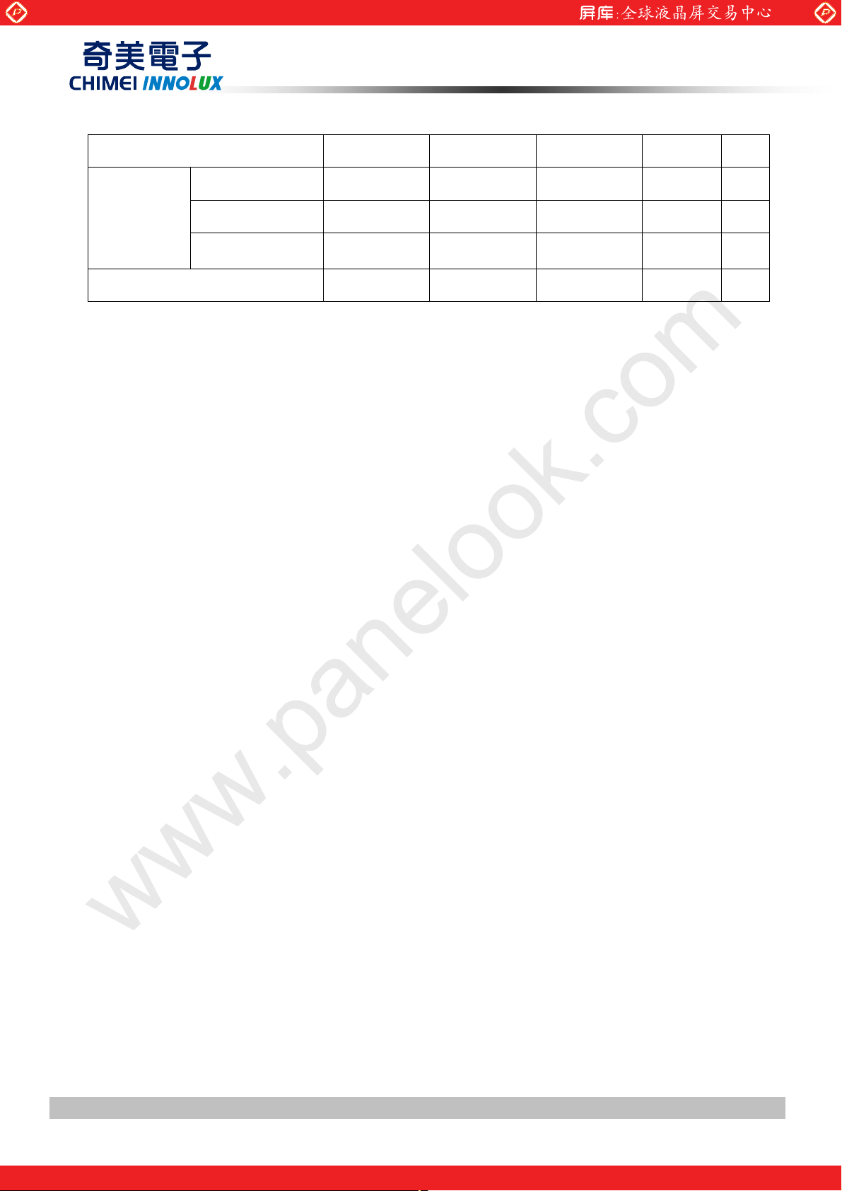
2. ABSOLUTE MAXIMUM RATINGS
2.1 ABSOLUTE RATINGS OF ENVIRONMENT
Item Symbol
Storage Temperature TST -20 +60 ºC (1)
Operating Ambient Temperature TOP 0 50 ºC (1), (2)
Shock (Non-Operating) SNOP - 50 G (3), (5)
Vibration (Non-Operating) VNOP - 1.0 G (4), (5)
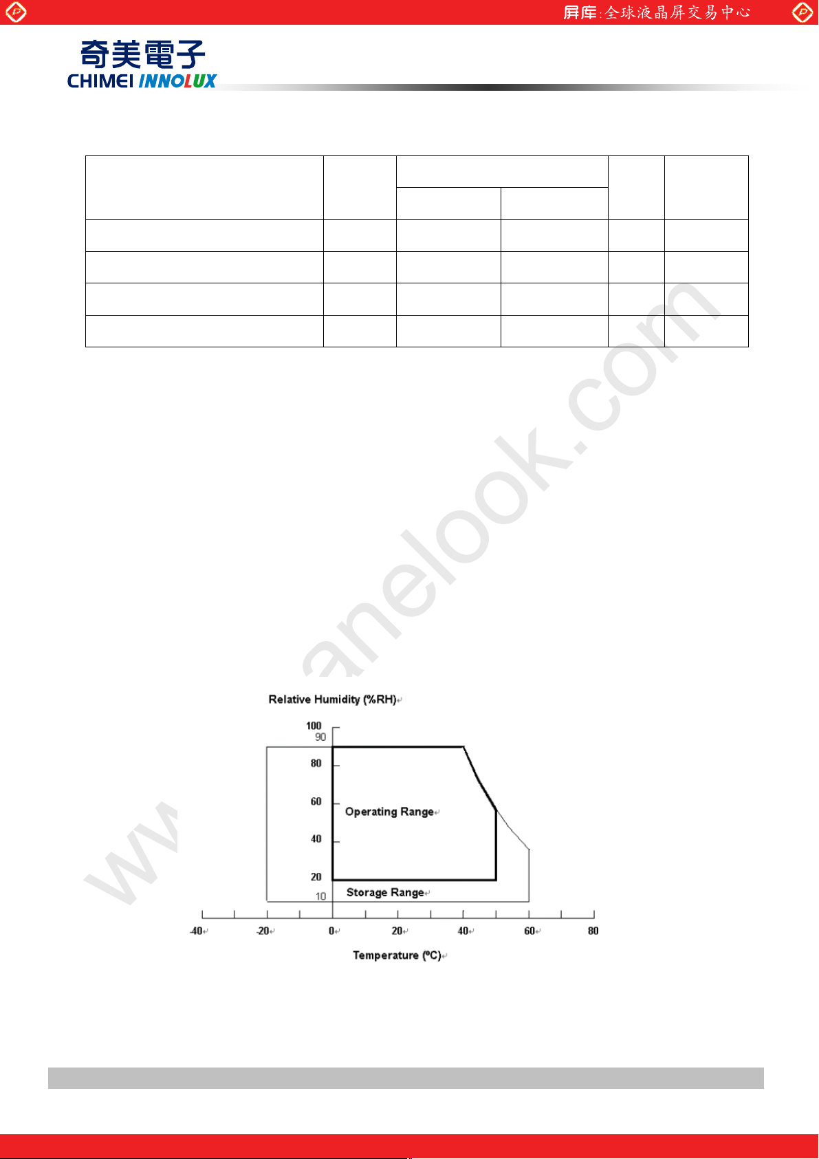
Note (1) Temperature and relative humidity range is shown in the figure below.
(a) 90 %RH Max. (Ta Љ 40 ºC).
(b) Wet-bulb temperature should be 39 ºC Max. (Ta > 40 ºC).
www.panelook.com
PRODUCT SPECIFICATION
Value
Unit Note
Min. Max.
(c) No condensation.
Note (2) The maximum operating temperature is based on the test condition that the surface temperature of
display area is less than or equal to 65 ºC with LCD module alone in a temperature controlled chamber.
Thermal management should be considered in final product design to prevent the surface temperature
of display area from being over 65 ºC. The range of operating temperature may degrade in case of
improper thermal management in final product design.
Note (3) 11 ms, half sine wave, 1 time for ± X, ± Y, ± Z.
Note (4) 10 ~ 200 Hz, 10 min, 1 time each X, Y, Z.
Note (5) At testing Vibration and Shock, the fixture in holding the module has to be hard and rigid enough so that
the module would not be twisted or bent by the fixture.
Version 2.1 7 DateΚΚΚΚ22 Sept 2010
The copyright belongs to CHIMEI InnoLux. Any unauthorized use is prohibited
One step solution for LCD / PDP / OLED panel application: Datasheet, inventory and accessory!
www.panelook.com
Page 8
Global LCD Panel Exchange Center
2.2 PACKAGE STORAGE
When storing modules as spares for a long time, the following precaution is necessary.
(a) Do not leave the module in high temperature, and high humidity for a long time, It is highly recommended to
store the module with temperature from 0 to 35 к at normal humidity without condensation.
(b) The module shall be stored in dark place. Do not store the TFT-LCD module in direct sunlight or fluorescent
light.
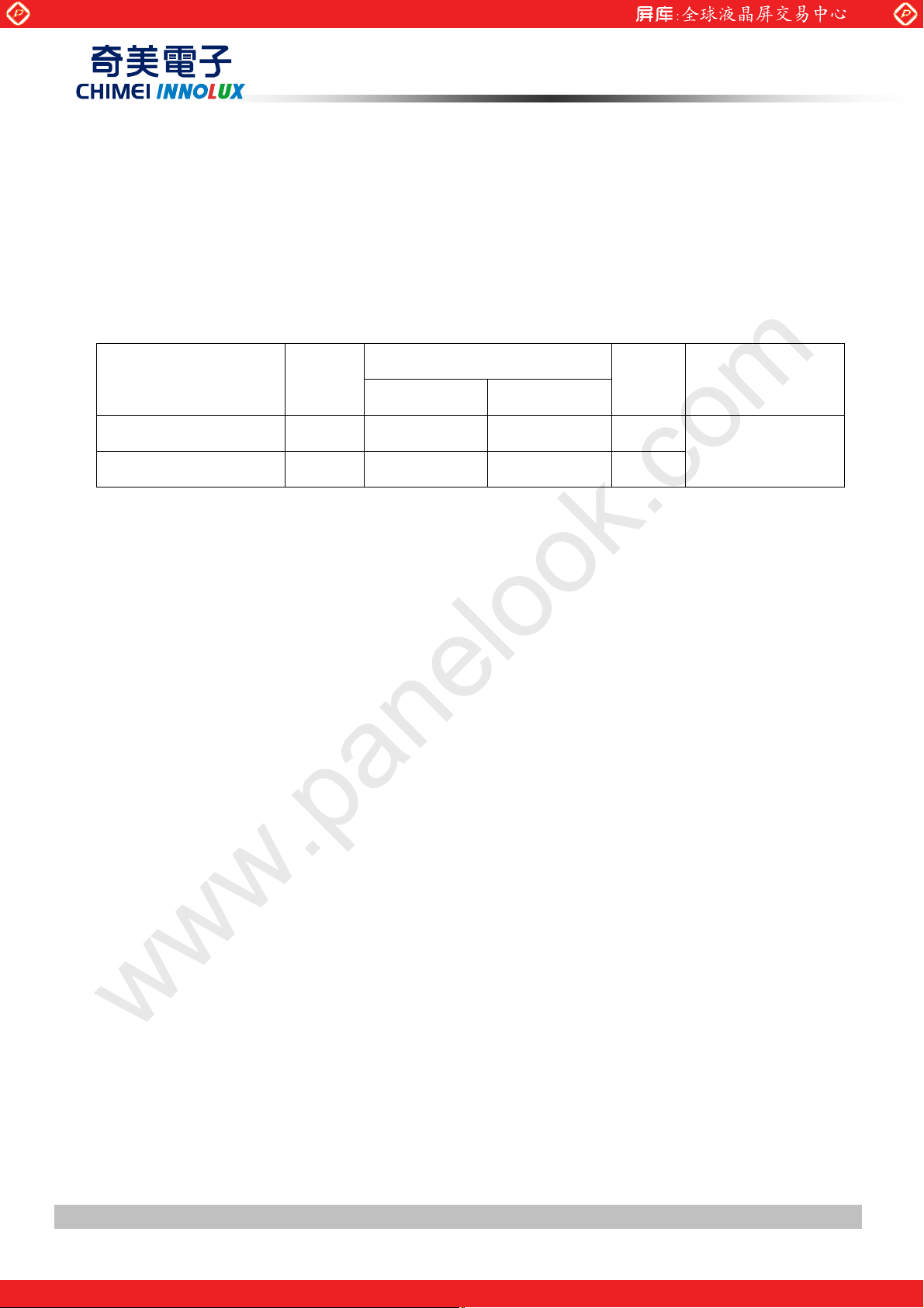
2.3 ELECTRICAL ABSOLUTE RATINGS
2.3.1 TFT LCD MODULE
Item Symbol
Power Supply Voltage VCC -0.3 13.5 V
Logic Input Voltage VIN -0.3 3.6 V
www.panelook.com
PRODUCT SPECIFICATION
Value
Unit Note
Min. Max.
(1)
Version 2.1 8 DateΚΚΚΚ22 Sept 2010
The copyright belongs to CHIMEI InnoLux. Any unauthorized use is prohibited
One step solution for LCD / PDP / OLED panel application: Datasheet, inventory and accessory!
www.panelook.com
Page 9
Global LCD Panel Exchange Center
3. ELECTRICAL CHARACTERISTICS
3.1 TFT LCD MODULE
Parameter Symbol
Power Supply Voltage VCC 4.5 5.0 5.5 V (1)
www.panelook.com
PRODUCT SPECIFICATION
(Ta = 25 ± 2 ºC)
Value
Unit Note
Min. Typ. Max.
Rush Current I
Power consumption P
White Pattern
Power Supply Current
Differential Input High
Threshold Voltage
Differential Input Low
LVDS
interface
Note (1) The module should be always operated within the above ranges.
Note (2) Even though Inrush current is over the specified value, there is no problem if I2T of fuse Spec is
Threshold Voltage
Common Input Voltage VCM 1.0 1.2 1.4 V
Differential input voltage
(single-end)
satisfied. The measurement condition is shown as bellowing.
Vertical Strip(MNT)
Black Pattern
RUSH
T
Ё
Ё
Ё
V
LVTH
V
LVTL
|V
| 200
ID
ЁЁ
Ё
- 0.51 0.61 A
- 1.06 1.26 A
- 1.05 1.26 A
+100
ЁЁ
5.3 6.3 (3)
ЁЁ
Ё
3 A (2)
mV
-100 mV
600 mV
(4)
(5)
Version 2.1 9 DateΚΚΚΚ22 Sept 2010
The copyright belongs to CHIMEI InnoLux. Any unauthorized use is prohibited
One step solution for LCD / PDP / OLED panel application: Datasheet, inventory and accessory!
www.panelook.com
Page 10
Global LCD Panel Exchange Center
GND
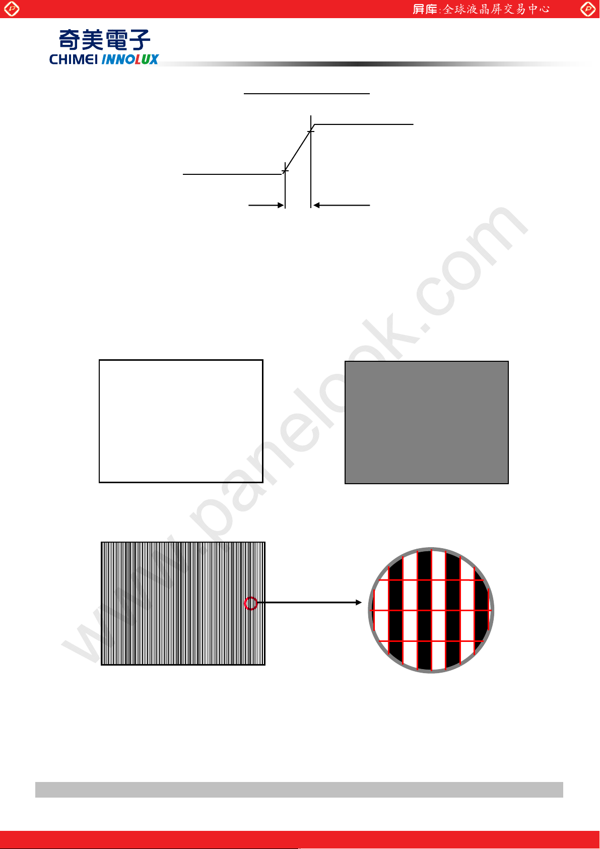
Note (3) The Specified Power consumption is under Vertical Stripe pattern.
www.panelook.com
PRODUCT SPECIFICATION
Vcc rising time is 470us
Vcc
0.9Vcc
0.1Vcc
470us
Note (4) The specified power supply current is under the conditions at Vcc=5.0V, Ta = 25 ± 2 ºC, f
whereas a power dissipation check pattern below is displayed.
a. White Pattern
Active Area
c. Vertical Stripe Pattern
b. Black Pattern
Active Area
G
R
B
R
= 60 Hz,
v
B
G
R
B
G
R
B
G
B
G
Active Area
G
B
R
G
B
R
G
R R
B
R
B
R
B
Version 2.1 10 DateΚΚΚΚ22 Sept 2010
The copyright belongs to CHIMEI InnoLux. Any unauthorized use is prohibited
One step solution for LCD / PDP / OLED panel application: Datasheet, inventory and accessory!
www.panelook.com
Page 11

Global LCD Panel Exchange Center
Note (5) The LVDS input characteristics are as follows :
www.panelook.com
PRODUCT SPECIFICATION
3.2 BACKLIGHT CONNECTOR PIN CONFIGURATION
3.2.1 LED LIGHT BAR CHARACTERISTICS
(Ta = 25 ± 2 ºC)
Parameter Symbol
Light Bar Voltage V
Forward Voltage V
LED Current I
Power consumption P
Life time -
Min. Typ. Max.
W
f
L
BL
- 40.3 44.2
- 3.1 3.4
--- 40 50
--- 9.7 13.3
30,000 - -
Value
Unit Note
V
V I
Duty=100%,
I
=40mA
L
=40mA
L
(1), (2)
mA
W
Duty=100%
Duty=100%,
I
=40mA
L
Hrs (3)
Note (1)LED light bar input voltage and current are measured by utilizing a true RMS multimeter as shown
below:
Note (2) P
= I
PIN
× V
BL
× ( 6 ) input pins , LED light bar circuit is (13)Series, (6)Parallel.
PIN
Note (3)The lifetime of LED is defined as the time when LED packages continue to operate under the
conditions at Ta = 25 ±2 and I= (20)mA (per chip) until the brightness becomes 50% of its кЉ
(1),
(1)
original value.
Power supply
V
PIN1, IPIN1
LED Backlight Module
CMO Converter
With PWM
Function
V
PIN(6) , IPIN(6)
Series:(13)
Parallel:(6)
Function
generator
Version 2.1 11 DateΚΚΚΚ22 Sept 2010
The copyright belongs to CHIMEI InnoLux. Any unauthorized use is prohibited
One step solution for LCD / PDP / OLED panel application: Datasheet, inventory and accessory!
www.panelook.com
Page 12

Global LCD Panel Exchange Center
www.panelook.com
PRODUCT SPECIFICATION
3.2.2 LIGHTBAR Connector Pin Assignment
The pin configuration for the housing and the leader wire is shown in the table below.
Connector: B-F,7083K-F12N-00L ,ENTERY(ܓ), or Compatible
Pin
1 NC No connect
2 LED1 LED1 negative polarity
3 LED2 LED2 negative polarity
4 LED3 LED3 negative polarity
5 NC No connect
6
7 VLED (41.6V) Input voltage Power Supply + (41.6V.typ)
8 NC No connect
9 LED4 LED4 negative polarity
10 LED5 LED5 negative polarity
11 LED6 LED6 negative polarity
12 NC No connect
3.3 LVDS INPUT SIGNAL SPECIFICATIONS
VLED (41.6V) Input voltage Power Supply + (41.6V.typ)
Symbol Feature
Version 2.1 12 DateΚΚΚΚ22 Sept 2010
The copyright belongs to CHIMEI InnoLux. Any unauthorized use is prohibited
One step solution for LCD / PDP / OLED panel application: Datasheet, inventory and accessory!
www.panelook.com
Page 13

Global LCD Panel Exchange Center
3.3.1 LVDS DATA MAPPING TABLE
LVDS Channel O0
LVDS Channel O1
LVDS Channel O2
LVDS Channel O3
LVDS Channel E0
LVDS Channel E1
LVDS Channel E2
LVDS Channel E3
LVDS output D7 D6 D4 D3 D2 D1 D0
Data order OG0 OR5 OR4 OR3 OR2 OR1 OR0
LVDS output D18 D15 D14 D13 D12 D9 D8
Data order OB1 OB0 OG5 OG4 OG3 OG2 OG1
LVDS output D26 D25 D24 D22 D21 D20 D19
Data order DE NA NA OB5 OB4 OB3 OB2
LVDS output D23 D17 D16 D11 D10 D5 D27
Data order NA OB7 OB6 OG7 OG6 OR7 OR6
LVDS output D7 D6 D4 D3 D2 D1 D0
Data order EG0 ER5 ER4 ER3 ER2 ER1 ER0
LVDS output D18 D15 D14 D13 D12 D9 D8
Data order EB1 EB0 EG5 EG4 EG3 EG2 EG1
LVDS output D26 D25 D24 D22 D21 D20 D19
Data order DE NA NA EB5 EB4 EB3 EB2
LVDS output D23 D17 D16 D11 D10 D5 D27
Data order NA EB7 EB6 EG7 EG6 ER7 ER6
www.panelook.com
PRODUCT SPECIFICATION
Version 2.1 13 DateΚΚΚΚ22 Sept 2010
The copyright belongs to CHIMEI InnoLux. Any unauthorized use is prohibited
One step solution for LCD / PDP / OLED panel application: Datasheet, inventory and accessory!
www.panelook.com
Page 14

Global LCD Panel Exchange Center
4. BLOCK DIAGRAM OF INTERFACE
4.1 TFT LCD MODULE
RXO0(+/-)
RXO1(+/-)
RXO2(+/-)
RXOC(+/-)
RXO3(+/-)
RXE0(+/-)
RXE1(+/-)
RXE2(+/-)
RXEC(+/-)
RXE3(+/-)
NC
Vcc
GND
www.panelook.com
PRODUCT SPECIFICATION
Version 2.1 14 DateΚΚΚΚ22 Sept 2010
The copyright belongs to CHIMEI InnoLux. Any unauthorized use is prohibited
One step solution for LCD / PDP / OLED panel application: Datasheet, inventory and accessory!
www.panelook.com
Page 15

Global LCD Panel Exchange Center
5. INPUT TERMINAL PIN ASSIGNMENT
5.1 TFT LCD Module Input
Pin Name Description
1 RXO0- Negative LVDS differential data input. Channel O0 (odd)
2 RXO0+ Positive LVDS differential data input. Channel O0 (odd)
3 RXO1- Negative LVDS differential data input. Channel O1 (odd)
4 RXO1+ Positive LVDS differential data input. Channel O1 (odd)
5 RXO2- Negative LVDS differential data input. Channel O2 (odd)
6 RXO2+ Positive LVDS differential data input. Channel O2 (odd)
7 GND Ground
8 RXOC- Negative LVDS differential clock input. (odd)
9 RXOC+ Positive LVDS differential clock input. (odd)
10 RXO3- Negative LVDS differential data input. Channel O3(odd)
11 RXO3+ Positive LVDS differential data input. Channel O3 (odd)
12 RXE0- Negative LVDS differential data input. Channel E0 (even)
13 RXE0+ Positive LVDS differential data input. Channel E0 (even)
14 GND Ground
15 RXE1- Negative LVDS differential data input. Channel E1 (even)
16 RXE1+ Positive LVDS differential data input. Channel E1 (even)
17 GND Ground
18 RXE2- Negative LVDS differential data input. Channel E2 (even)
19 RXE2+ Positive LVDS differential data input. Channel E2 (even)
20 RXEC- Negative LVDS differential clock input. (even)
21 RXEC+ Positive LVDS differential clock input. (even)
22 RXE3- Negative LVDS differential data input. Channel E3 (even)
23 RXE3+ Positive LVDS differential data input. Channel E3 (even)
24 GND Ground
25 NC Not connection, this pin should be open.
26 NC CMI internal test, this pin should connect to ground.
27 NC Not connection, this pin should be open.
28 VCC +5.0V power supply
29 VCC +5.0V power supply
30 VCC +5.0V power supply
Note (1) Connector Part No.: 093G30-B2001A-M4(STARCONN) or MSCKT2407P30H,STM(ฐ)
www.panelook.com
PRODUCT SPECIFICATION
Note (2) Mating Wire Cable Connector Part No.: FI-X30H(JAE) or FI-X30HL(JAE)
Note (3) Mating FFC Cable Connector Part No.: B-F,7083K-F12N-00L ,ENTERY(ܓ)
Note (4) The first pixel is odd.
Note (5) Input signal of even and odd clock should be the same timing.
Version 2.1 15 DateΚΚΚΚ22 Sept 2010
The copyright belongs to CHIMEI InnoLux. Any unauthorized use is prohibited
One step solution for LCD / PDP / OLED panel application: Datasheet, inventory and accessory!
www.panelook.com
Page 16

Global LCD Panel Exchange Center
G0-EG
r
K
K
5.2 BLOCK DIAGRAM OF INTERFACE
CN1
www.panelook.com
PRODUCT SPECIFICATION
ARx0-
ARx0+
ARx1-
ARx1+
ARx2-
ARx2+
ACL
ACLK+
ARx3-
ARx3+
BRx0-
BRx0+
BRx1-
BRx1+
100Ө
ER0-ER7
100Ө
E
7
EB0-EB7
-
100Ө
100Ө
DE
OR0-OR7
OG0-OG7
100Ө
PLL
100Ө
100Ө
OB0-OB7
DCLK
BRx2-
BRx2+
BCL
-
100Ө
100Ө
BCLK+
BRx3-
BRx3+
100Ө
PLL
Timing
Controlle
Version 2.1 16 DateΚΚΚΚ22 Sept 2010
The copyright belongs to CHIMEI InnoLux. Any unauthorized use is prohibited
One step solution for LCD / PDP / OLED panel application: Datasheet, inventory and accessory!
www.panelook.com
Page 17

Global LCD Panel Exchange Center
www.panelook.com
PRODUCT SPECIFICATION
ER0~ER7 Even pixel R data OR0~OR7 Odd pixel R data
EG0~EG7 Even pixel G data OG0~OG7 Odd pixel G data
EB0~EB7 Even pixel B data OB0~OB7 Odd pixel B data
DE Data enable signal
DCLK Data clock signal
Note (1) The system must have the transmitter to drive the module.
Note (2) LVDS cable impedance shall be 50 ohms per signal line or about 100 ohms per twist-pair line when
it is used differentially.
Note (3) Two pixel data send into the module for every clock cycle. The first pixel of the frame is odd pixel
and the second pixel is even pixel.
Version 2.1 17 DateΚΚΚΚ22 Sept 2010
The copyright belongs to CHIMEI InnoLux. Any unauthorized use is prohibited
One step solution for LCD / PDP / OLED panel application: Datasheet, inventory and accessory!
www.panelook.com
Page 18

Global LCD Panel Exchange Center
5.3 LVDS INTERFACE
VESA Format : SELLVDS = L or Open
www.panelook.com
PRODUCT SPECIFICATION
AR0~AR9 : First Pixel R Data (9; MSB, 0; LSB)
AG0~AG9 : First Pixel G Data (9; MSB, 0; LSB)
AB0~AB9 : First Pixel B Data (9; MSB, 0; LSB)
DE : Data enable signal
DCLK : Data clock signal
RSVD : Reserved
Version 2.1 18 DateΚΚΚΚ22 Sept 2010
The copyright belongs to CHIMEI InnoLux. Any unauthorized use is prohibited
One step solution for LCD / PDP / OLED panel application: Datasheet, inventory and accessory!
www.panelook.com
Page 19

Global LCD Panel Exchange Center
5.4 COLOR DATA INPUT ASSIGNMENT
The brightness of each primary color (red, green and blue) is based on the 8-bit gray scale data input for the
color. The higher the binary input, the brighter the color. The table below provides the assignment of color
versus data input.
Color
R7 R6 R5 R4 R3 R2 R1 R0 G7 G6 G5 G4 G3 G2 G1 G0 B7 B6 B5 B4 B3 B2 B1 B0
0
0
0
1
1
1
0
0
0
0
0
0
0
0
0
1
1
1
1
1
1
1
1
1
0
0
0
0
0
0
0
0
0
:
:
:
:
1
1
1
1
1
1
1
1
1
Basic
Colors
Gray
Scale
Of
Red
Black
Red
Green
Blue
Cyan
Magenta
Yel lo w
White
Red(0) / Dark
Red(1)
Red(2)
:
:
Red(253)
Red(254)
Red(255)
www.panelook.com
PRODUCT SPECIFICATION
Data Signal
Red Green Blue
0
0
0
0
0
0
0
0
0
0
0
0
0
0
0
0
0
0
0
0
0
0
0
0
0
0
0
0
0
0
0
0
0
0
0
0
0
1
1
1
1
1
0
0
0
0
0
0
0
0
1
1
1
1
1
1
1
1
0
0
0
0
0
1
1
1
1
1
1
1
0
0
0
0
0
0
0
0
0
0
0
0
0
1
1
1
1
1
1
1
1
1
1
1
1
1
0
0
0
0
0
1
1
1
1
1
0
0
0
0
0
0
0
0
1
1
1
1
1
0
0
0
0
0
1
1
1
1
1
1
1
1
1
1
1
1
1
1
1
1
1
1
1
1
1
1
1
1
1
1
1
1
1
1
1
0
0
0
0
0
0
0
0
0
0
0
0
0
0
0
0
0
0
0
0
1
0
0
0
0
0
0
0
0
0
0
0
0
1
0
0
0
:
:
:
:
:
:
:
:
:
:
:
:
:
:
:
:
:
:
:
:
:
:
:
:
:
:
0
0
0
0
0
0
0
1
0
1
1
1
0
0
0
0
0
0
0
0
1
1
1
1
0
0
0
0
0
0
0
1
1
1
1
1
0
0
0
0
0
:
:
0
0
0
0
0
0
0
0
0
0
0
0
:
:
:
:
:
:
0
0
0
0
0
0
0
0
0
0
0
0
:
:
:
:
0
0
0
0
0
0
1
1
1
1
1
1
1
0
0
0
1
1
1
0
0
0
0
0
0
0
0
0
:
:
:
:
:
:
0
0
0
0
0
0
0
0
0
Green(0) / Dark
Green(1)
Gray
Scale
Of
Green
Gray
Scale
Of
Blue
Note (1) 0: Low Level Voltage, 1: High Level Voltage
Green(2)
:
:
Green(253)
Green(254)
Green(255)
Blue(0) / Dark
Blue(1)
Blue(2)
:
:
Blue(253)
Blue(254)
Blue(255)
0
0
0
0
0
0
0
0
0
0
0
0
0
0
0
:
:
:
:
:
:
:
:
:
:
:
:
:
:
0
0
0
0
0
0
0
0
0
0
0
0
0
0
0
0
0
0
0
0
0
0
0
0
0
0
0
0
0
0
0
0
0
0
0
0
0
0
0
0
0
0
:
:
:
:
:
:
:
:
:
:
:
:
:
:
0
0
0
0
0
0
0
0
0
0
0
0
0
0
0
0
0
0
0
0
0
0
0
0
0
0
0
0
0
0
0
1
0
0
0
0
0
0
0
0
0
0
0
0
1
0
0
0
0
0
0
0
:
:
:
:
:
:
:
:
:
:
:
:
:
:
:
:
:
:
:
:
:
:
:
0
1
0
1
1
1
1
1
1
0
0
0
1
1
1
1
1
1
1
0
0
1
1
1
1
1
1
1
1
0
0
0
0
0
0
0
0
0
0
0
0
0
0
0
0
0
0
0
0
0
0
0
0
0
0
:
:
:
:
:
:
:
:
:
:
:
:
:
:
:
:
0
0
0
0
0
0
0
0
0
0
0
0
0
0
0
0
0
0
0
0
0
0
0
0
0
0
0
0
0
:
:
:
:
1
0
1
0
1
0
:
0
0
0
0
0
0
0
0
0
0
0
0
:
:
:
:
1
1
1
1
1
1
0
0
0
0
0
0
:
:
:
:
0
0
0
0
0
0
0
0
0
0
0
0
:
:
:
:
1
1
1
1
1
1
0
0
0
0
0
0
0
0
0
:
:
:
:
:
:
0
0
0
0
0
0
0
0
0
0
0
0
1
0
0
0
1
0
:
:
:
:
:
:
1
0
1
0
1
1
1
1
1
0
0
0
0
0
0
0
0
0
0
0
Version 2.1 19 DateΚΚΚΚ22 Sept 2010
The copyright belongs to CHIMEI InnoLux. Any unauthorized use is prohibited
One step solution for LCD / PDP / OLED panel application: Datasheet, inventory and accessory!
www.panelook.com
Page 20

Global LCD Panel Exchange Center
6. INTERFACE TIMING
6.1 INPUT SIGNAL TIMING SPECIFICATIONS
The input signal timing specifications are shown as the following table and timing diagram. (Ta = 25 ± 2 ºC)
Signal Item Symbol Min. Typ. Max. Unit Note
F
(=1/TC)
clkin_mod
F
F
LVDS
Receiver
Clock
Frequency
Input cycle to
cycle jitter
Spread spectrum
modulation range
Spread spectrum
modulation frequency
www.panelook.com
PRODUCT SPECIFICATION
clkin
T
SSM
rcl
58.54 74.25 97.98 MHz
ЁЁ
F
-2%
clkin
Ё
200 ps (2)
F
+2% MHz
clkin
200 KHz
(3)
LVDS
Setup Time Tlvsu 600
ЁЁ
ps
Receiver
Data
Hold Time Tlvhd 600
ЁЁ
ps
Frame Rate Fr 50 60 75 Hz
Ver t ical
Active
Display
Term
Total Tv 1115 1125 1136 Th
Display Tvd 1080 1080 1080 Th
Tv=Tvd+Tvb
Blank Tvb Tv-Tvd 45 Tv-Tvd Th
Horizontal
Active
Display
Term
Total Th 1050 1100 1150 Tc
Display Thd 960 960 960 Tc
Blank Thb Th-Thd 140 Th-Thd Tc
Th=Thd+Thb
Note: Because this module is operated by DE only mode, Hsync and Vsync input signals are ignored.
INPUT SIGNAL TIMING DIAGRAM
Version 2.1 20 DateΚΚΚΚ22 Sept 2010
The copyright belongs to CHIMEI InnoLux. Any unauthorized use is prohibited
One step solution for LCD / PDP / OLED panel application: Datasheet, inventory and accessory!
www.panelook.com
Page 21

Global LCD Panel Exchange Center
www.panelook.com
PRODUCT SPECIFICATION
Note (1) Please make sure the range of frame rate has follow the below equationΚ
Fr(max) Fclkin Њ Я Tv×Th Fr(min)Љ
Note (2) The input clock cycle-to-cycle jitter is defined as below figures. Trcl = I T
Note (3) The SSCG (Spread spectrum clock generator) is defined as below figures.
– TI
1
Version 2.1 21 DateΚΚΚΚ22 Sept 2010
The copyright belongs to CHIMEI InnoLux. Any unauthorized use is prohibited
One step solution for LCD / PDP / OLED panel application: Datasheet, inventory and accessory!
www.panelook.com
Page 22

Global LCD Panel Exchange Center
www.panelook.com
PRODUCT SPECIFICATION
6.2 POWER ON/OFF SEQUENCE
To prevent a latch-up or DC operation of LCD module, the power on/off sequence should be as the
diagram below.
Timing Specifications:
0.5 < t1 Љ 10 msec
0 < t2 Љ 50 msec
0 < t3 Љ 50 msec
t4 Њ 500 msec
t5 Њ 450 msec
t6 Њ 90 msec
5 Љ t7 Љ 100 msec
Note.
(1) The supply voltage of the external system for the module input should be the same as the definition of Vcc.
(2) When the backlight turns on before the LCD operation of the LCD turns off, the display may momentarily
become abnormal screen.
(3) In case of Vcc = off level, please keep the level of input signals on the low or keep a high impedance.
(4) t4 should be measured after the module has been fully discharged between power of and on period.
(5) Interface signal shall not be kept at high impedance when the power is on.
(6) CMO won’t take any responsibility for the products which are damaged by the customers not following the
Power Sequence.
(7) There might be slight electronic noise when LCD is turned off (even backlight unit is also off). To avoid this
symptom, we suggest "Vcc falling timing" to follow "t7 spec".
Version 2.1 22 DateΚΚΚΚ22 Sept 2010
The copyright belongs to CHIMEI InnoLux. Any unauthorized use is prohibited
One step solution for LCD / PDP / OLED panel application: Datasheet, inventory and accessory!
www.panelook.com
Page 23

Global LCD Panel Exchange Center
7. OPTICAL CHARACTERISTICS
7.1 TEST CONDITIONS
Item Symbol Value Unit
www.panelook.com
PRODUCT SPECIFICATION
Ambient Temperature Ta
Ambient Humidity Ha
Supply Voltage VCC 5 V
Input Signal According to typical value in "3. ELECTRICAL CHARACTERISTICS"
LED Current IL 40 ± 0.6 mA
The LCD module should be stabilized at given temperature for 1 hour to avoid abrupt temperature change during
measuring. In order to stabilize the luminance, the measurement should be executed after lighting backlight for 1
hour in a windless room.
25±2
50±10
oC
%RH
Version 2.1 23 DateΚΚΚΚ22 Sept 2010
The copyright belongs to CHIMEI InnoLux. Any unauthorized use is prohibited
One step solution for LCD / PDP / OLED panel application: Datasheet, inventory and accessory!
www.panelook.com
Page 24

Global LCD Panel Exchange Center
7.2 OPTICAL SPECIFICATIONS
The relative measurement methods of optical characteristics are shown in 7.2. The following items should be
measured under the test conditions described in 7.1 and stable environment shown in 7.1.
Item Symbol Condition Min. Typ. Max. Unit Note
Contrast Ratio CR 700 1000 - - Note (2)
www.panelook.com
PRODUCT SPECIFICATION
Response Time
T
R
T
F
- 1.3 2.2
ms Note (3)
- 3.7 5.8
Center Luminance of White LC 200 250 - cd/m2Note (5)
White Variation
δW
- - 1.3 - Note (7)
Cross Talk CT - - 4 % Note (6)
Rx 0.644 -
Red
Ry 0.338 -
θx=0°, θy =0°
Viewing angle
at normal direction
Gx 0.310 -
Green
Color
Chromaticity
Gy 0.619 -
Bx 0.153 -
Blue
Typ.
-0.03
Typ.
+0.03
(1)(4)
By 0.062 -
Wx 0.313 -
White
Wy
0.329
-
Viewing Angle
Color Gamut C.G
Horizontal
Ver t ical
Horizontal
Ver t ical
θ
+ + θx-
x
θ
++ θY-
Y
θ
+ + θx-
x
θ
++ θY-
Y
CR 10Њ
USB2000
CR 5Њ
USB2000
- 70 - % NTSC
150 170 -
140 160 -
Deg. (1)(4)
160 178 -
150 170 -
Version 2.1 24 DateΚΚΚΚ22 Sept 2010
The copyright belongs to CHIMEI InnoLux. Any unauthorized use is prohibited
One step solution for LCD / PDP / OLED panel application: Datasheet, inventory and accessory!
www.panelook.com
Page 25

Global LCD Panel Exchange Center
Note (1) Definition of Viewing Angle (θx, θy) :
www.panelook.com
PRODUCT SPECIFICATION
Normal
θx = θy = 0º
θX- = 90º
6 o’clock
θy- = 90º
x-
y-
Note (2) Definition of Contrast Ratio (CR) :
The contrast ratio can be calculated by the following expression.
Contrast Ratio (CR) =
CR = CR (5), where CR (X) is corresponding to the Contrast Ratio of the point X at the figure in Note(6).
Note (3) Definition of Response Time (T
R
θy- θy+
θx−
, TF):
θx+
12 o’clock direction
θy+ = 90º
y+
pixels whiteall withLuminance Surface
pixels black all withLuminance Surface
x+
θX+ = 90º
100%
90%
Optical
Response
10%
0%
Gray Level 255
T
R
66.67ms
Gray Level 0
T
F
66.67ms
Gray Level 255
Time
Version 2.1 25 DateΚΚΚΚ22 Sept 2010
The copyright belongs to CHIMEI InnoLux. Any unauthorized use is prohibited
One step solution for LCD / PDP / OLED panel application: Datasheet, inventory and accessory!
www.panelook.com
Page 26

Global LCD Panel Exchange Center
A
(
)
A
(
)
Note (4) Measurement Setup:
The LCD module should be stabilized at given temperature for 1 hour to avoid abrupt
temperature change during measuring. In order to stabilize the luminance, the measurement
should be executed after lighting backlight for 1 hour in a windless room.
LCD M odule
LCD P anel
www.panelook.com
PRODUCT SPECIFICATION
Note (5) Definition of Luminance of White (L
Measure the luminance of gray level 255 at center point and 5 points
L
= L (5), where L (X) is corresponding to the luminance of the point X at the figure in Note (6).
C
Note (6) Definition of Cross Talk (CT):
CT = | YB – YA | / YA × 100 (%)
Where:
YA = Luminance of measured location without gray level 0 pattern (cd/m2)
YB = Luminance of measured location with gray level 0 pattern (cd/m2)
500 mm
CS -2000
Light Shield Room
(Ambient Luminance < 2 lux)
, L
):
C
AVE
(0, 0)
(D/8,W/2)
Y
A, L
ctive Area
Gray 128
(D/2,7W/8)
Y
A, D
Y
(D/2,W/8)
A, U
Y
(7D/8,W/2)
A, R
D, W
(0, 0)
(D/8,W/2)
Y
B, L
ctive Area
Gray 0
(D/2,7W/8)
Y
B, D
(D/2,W/8)
Y
B, U
Note (7) Definition of White Variation (δW):
Measure the luminance of gray level 255 at 5 points
δW = Maximum [L (1), L (2), L (3), L (4), L (5)] / Minimum [L (1), L (2), L (3), L (4), L (5)]
Version 2.1 26 DateΚΚΚΚ22 Sept 2010
The copyright belongs to CHIMEI InnoLux. Any unauthorized use is prohibited
One step solution for LCD / PDP / OLED panel application: Datasheet, inventory and accessory!
Y
(7D/8,W/2)
B, R
D, W
www.panelook.com
Page 27

Global LCD Panel Exchange Center
www.panelook.com
PRODUCT SPECIFICATION
8. PRECAUTIONS
8.1 ASSEMBLY AND HANDLING PRECAUTIONS
[ 1 ] Do not apply rough force such as bending or twisting to the module during assembly.
[ 2 ] It is recommended to assemble or to install a module into the user’s system in clean working areas. The
dust and oil may cause electrical short or worsen the polarizer.
[ 3 ] Do not apply pressure or impulse to the module to prevent the damage of LCD panel and Backlight.
[ 4 ] Always follow the correct power-on sequence when the LCD module is turned on. This can prevent the
damage and latch-up of the CMIS LSI chips.
[ 5 ] Bezel of Set can not press or touch the panel surface. It will make light leakage or scrape.
[ 6 ] Do not plug in or pull out the I/F connector while the module is in operation.
[ 7 ] Do not disassemble the module.
[ 8 ] Use a soft dry cloth without chemicals for cleaning, because the surface of polarizer is very soft and easily
scratched.
[ 9 ] Moisture can easily penetrate into LCD module and may cause the damage during operation.
[ 10 ] When storing modules as spares for a long time, the following precaution is necessary.
[ 10.1 ] Do not leave the module in high temperature, and high humidity for a long time. It is highly
recommended to store the module with temperature from 0 to 35кat normal humidity without
condensation.
[ 10.2 ] The module shall be stored in dark place. Do not store the TFT-LCD module in direct sunlight or
fluorescent light.
[ 11 ] When ambient temperature is lower than 10ºC, the display quality might be reduced. For example, the
response time will become slow, and the starting voltage of CCFL will be higher than that of room
temperature.
8.2 SAFETY PRECAUTIONS
[ 1 ] The startup voltage of a Backlight is approximately 1000 Volts. It may cause an electrical shock while
assembling with the inverter. Do not disassemble the module or insert anything into the Backlight unit.
[ 2 ] If the liquid crystal material leaks from the panel, it should be kept away from the eyes or mouth. In case of
contact with hands, skin or clothes, it has to be washed away thoroughly with soap.
[ 3 ] After the module’s end of life, it is not harmful in case of normal operation and storage.
Version 2.1 27 DateΚΚΚΚ22 Sept 2010
The copyright belongs to CHIMEI InnoLux. Any unauthorized use is prohibited
One step solution for LCD / PDP / OLED panel application: Datasheet, inventory and accessory!
www.panelook.com
Page 28

Global LCD Panel Exchange Center
9. DEFINITION OF LABELS
9.1 CMI MODULE LABEL
The barcode nameplate is pasted on each module as illustration, and its definitions are as following explanation.
www.panelook.com
PRODUCT SPECIFICATION
CHI MEI
OPTOELECTRONICS
CHI MEI
OPTOELECTRONICS
Model Name: V215H1 –LE1
Revision: Rev. XX, for example: A0, A1… B1, B2… or C1, C2…etc.
Serial ID: X X X X X X X Y M D L N N N N
V215H1 –LE1 Rev. XX
X X X X X X X Y M D L N N N N
V215H1 –LE1 Rev. XX
X X X X X X X Y M D L N N N N
Serial No.
E207943
MADE IN TAIWAN
GEMN
RoHS
MADE IN CHINA
LEOO(or CAPG or CANO)
RoHS
Product Line
Year, Month, Date
CMI Internal Use
CMI Internal Use
Revision
Serial ID includes the information as below:
Manufactured Date:
Year : 2001=1, 2002=2, 2003=3, 2004=4…2010=0, 2011=1, 2012=2…
Month: 1~9, A~C, for Jan. ~ Dec.
Day: 1~9, A~Y, for 1st to 31st, exclude I ,O, and U.
Revision Code : Cover all the change
Serial No. : Manufacturing sequence of product
Product Line : 1 → Line1, 2 → Line 2, …etc.
CMI Internal Use
Version 2.1 28 DateΚΚΚΚ22 Sept 2010
The copyright belongs to CHIMEI InnoLux. Any unauthorized use is prohibited
One step solution for LCD / PDP / OLED panel application: Datasheet, inventory and accessory!
www.panelook.com
Page 29

Global LCD Panel Exchange Center
10. PACKAGING
10.1 PACKAGING SPECIFICATIONS
(1) 13 LCD modules / 1 Box
(2) Box dimensions: 567(L) X 301(W) X 376(H) mm
(3) Weight: 27.525kg (13 modules per box)
10.2 PACKAGING METHOD
Figures 10-1 and 10-2 are the packing method
www.panelook.com
PRODUCT SPECIFICATION
Figure 10-1 packing method
Version 2.1 29 DateΚΚΚΚ22 Sept 2010
The copyright belongs to CHIMEI InnoLux. Any unauthorized use is prohibited
One step solution for LCD / PDP / OLED panel application: Datasheet, inventory and accessory!
www.panelook.com
Page 30

Global LCD Panel Exchange Center
Sea / Land Transportation
(40ft HQ Container)
www.panelook.com
PRODUCT SPECIFICATION
Sea / Land Transportation
(40ft Container)
Air Transportation
Figure 10-2 packing method
Version 2.1 30 DateΚΚΚΚ22 Sept 2010
The copyright belongs to CHIMEI InnoLux. Any unauthorized use is prohibited
One step solution for LCD / PDP / OLED panel application: Datasheet, inventory and accessory!
www.panelook.com
Page 31

Global LCD Panel Exchange Center
11. MECHANICAL CHARACTERISTIC
www.panelook.com
PRODUCT SPECIFICATION
Version 2.1 31 DateΚΚΚΚ22 Sept 2010
The copyright belongs to CHIMEI InnoLux. Any unauthorized use is prohibited
One step solution for LCD / PDP / OLED panel application: Datasheet, inventory and accessory!
www.panelook.com
Page 32

Global LCD Panel Exchange Center
www.panelook.com
PRODUCT SPECIFICATION
Version 2.1 32 DateΚΚΚΚ22 Sept 2010
The copyright belongs to CHIMEI InnoLux. Any unauthorized use is prohibited
One step solution for LCD / PDP / OLED panel application: Datasheet, inventory and accessory!
www.panelook.com
 Loading...