

Page 1
Global LCD Panel Exchange Center
A
TFT LCD Approval Specification
MODEL NO.: V201V2 - T03
www.panelook.com
Issued Date: Nov. 29, 2004
Model No.: V201V2 -T03
Approval
Customer: __
pproved by:
Note:
LCD TV Head Division
AVP
Version 2.1
One step solution for LCD / PDP / OLED panel application: Datasheet, inventory and accessory!
QRA Dept.
DDIII DDII DDI
Approval Approval Approval Approval
ຫةԫ ޕޫ ៴֮ᙘ ֮ࣥᜣ
LCD TV Marketing and Product Management Division
Product Manager
1
ພၼ
TVHD / PDD
ஊ壁 ຫمࡵ
www.panelook.com
Page 2
Global LCD Panel Exchange Center
www.panelook.com
Issued Date: Nov. 29, 2004
Model No.: V201V2 -T03
Approval
- CONTENTS -
REVISION HISTORY
1. GENERAL DESCRIPTION
1.1 OVERVIEW
1.2 FEATURES
1.3 APPLICATION
1.4 GENERAL SPECIFICATIONS
1.5 MECHANICAL SPECIFICATIONS
2. ABSOLUTE MAXIMUM RATINGS
2.1 ABSOLUTE RATINGS OF ENVIRONMENT
2.2 ELECTRICAL ABSOLUTE RATINGS
2.2.1 TFT LCD MODULE
2.2.2 BACKLIGHT INVERTER UNIT
3. ELECTRICAL CHARACTERISTICS
3.1 TFT LCD MODULE
3.2 BACKLIGHT UNIT
3.2.1 CCFL
3.2.2 INVERTER CHARACTERISTICS
3.2.3 INVERTER INTERTFACE CHARACTERISTICS
(Cold Cathode Fluorescent Lamp) CHARACTERISTICS
4. BLOCK DIAGRAM
4.1 TFT LCD MODULE
5. INTERFACE PIN CONNECTION
5.1 TFT LCD MODULE
5.2 COLOR DATA INPUT ASSIGNMENT
5.3 BACKLIGHT UNIT
5.4 INVERTER UNIT
6. INTERFACE TIMING
6.1 INPUT SIGNAL TIMING SPECIFICATIONS
6.2 POWER ON/OFF SEQUENCE
7. OPTICAL CHARACTERISTICS
7.1 TEST CONDITIONS
7.2 OPTICAL SPECIFICATIONS
8. PACKAGING ------------------------------------------------------- 23
8.1 PACKING SPECIFICATIONS
8.1 PACKING METHOD
9. DEFINITION OF LABELS ------------------------------------------------------- 25
9.1 CMO MODULE LABEL
10. PRECAUTIONS ------------------------------------------------------- 26
10.1 ASSEMBLY AND HANDLING PRECAUTIONS
10.2 SAFETY PRECAUTIONS
10.3 SAFETY REGULATION
------------------------------------------------------- 3
------------------------------------------------------- 4
------------------------------------------------------- 5
------------------------------------------------------- 7
------------------------------------------------------- 12
------------------------------------------------------- 13
------------------------------------------------------- 17
------------------------------------------------------- 19
11. MECHANICAL CHARACTERISTICS ------------------------------------------------------- 27
2
Version 2.1
One step solution for LCD / PDP / OLED panel application: Datasheet, inventory and accessory!
www.panelook.com
Page 3
Global LCD Panel Exchange Center
REVISION HISTORY
www.panelook.com
Issued Date: Nov. 29, 2004
Model No.: V201V2 -T03
Approval
Date
Oct. 05,’04
Nov. 01,’04
Nov.29,’04
Page
(New)
All
All
8
19
12
13
19
27
28
Section Description
Preliminary Specification was first issued.
All
Approval Specification was first issued.
All
3.2.1
7.2
4.1
5.1
Lamp Voltage Typ.웛815 Æ 840
Lamp Current Min.Κ4.0 Æ 4.2 , Max.Κ5.0 Æ 4.8
Lamp Starting Voltage(Ta = 0 ºC) Typ.Κ1650Æ - , Max.Κ- Æ 1730
Lamp Starting Voltage(Ta = 25 ºC) Typ.Κ1320Æ - , Max.Κ- Æ 1530
Contrast Ratio Min.Κ- Æ 800
Color ChromaticityΚ
Min. Typ. Max.
RxΚ0.616 Æ 0.622 0.646 Æ 0.652 0.676 Æ 0.682
RyΚ0.301 Æ 0.302 0.331 Æ 0.332 0.361 Æ 0.362
GxΚ0.238 Æ 0.243 0.268 Æ 0.273 0.298 Æ 0.303
GyΚ0.573 Æ
BxΚ0.113 Æ 0.112 0.143 Æ 0.142 0.173 Æ 0.172
ByΚ0.039 Æ 0.038 0.069 Æ 0.068 0.099 Æ 0.098
Input connectorΚHirose FH12-50S-0.5SHÆ P-TWO AF7501-N2G1Z
Connector Part No.Κ
FH12-50S-0.5SH(Hirose)Æ AF7501-N2G1Z (P-TWO)
7
Response Time was modified.
Notes were modified.
11
11
The Drawing was modified.
The Drawing was modified.
0.568 0.603 Æ 0.598 0.633 Æ 0.628
3
Version 2.1
One step solution for LCD / PDP / OLED panel application: Datasheet, inventory and accessory!
www.panelook.com
Page 4
Global LCD Panel Exchange Center
1. GENERAL DESCRIPTION
1.1 OVERVIEW
V201V2-T03 is a 20.1” TFT Liquid Crystal Display module with 12-CCFL Backlight unit and 1ch-TTL
interface. This module supports 640 x 480 VGA format and can display true 16.7M colors ( 8-bit/color). The
inverter module for backlight is built-in.
1.2 FEATURES
- High brightness ( 500 nits)
- High contrast ratio (1000:1)
- Fast response time
- High color saturation NTSC 75%
- VGA (640 x 480 pixels) resolution
www.panelook.com
Issued Date: Nov. 29, 2004
Model No.: V201V2 -T03
Approval
- DE (Data Enable) only mode
- TTL interface
1.3 APPLICATION
- TFT LCD display
1.4 GENERAL SPECIFICATI0NS
Item Specification Unit Note
Active Area 408 (H) x 306 (V) (20.1” diagonal) mm
Bezel Opening Area 412 (H) x 310 (V) mm
Driver Element a-si TFT active matrix - Pixel Number 640 x R.G.B. x 480 pixel Pixel Pitch(Sub Pixel) 0.2125 (H) x 0.6375 (V) mm Pixel Arrangement RGB vertical stripe - Display Colors 16.7M color Display Operation Mode Transmissive mode / Normally black - -
Surface Treatment
Hardness : 3H, Haze : 40%
Anti-reflective coating < 2% reflection
- -
1.5 MECHANICAL SPECIFICATIONS
Item Min. Typ. Max. Unit Note
Horizontal(H) 435.7 436.0 436.4 mm
Module Size
Note (1) Please refer to the attached drawings for more information of front and back outline dimensions.
Vertical(V) 329.0 329.3 329.7 mm
Depth(D) - 40.38 41.38 mm
Weight - 2200 2300 g
(1)
(1)
with INV
Cover
4
Version 2.1
One step solution for LCD / PDP / OLED panel application: Datasheet, inventory and accessory!
www.panelook.com
Page 5
Global LCD Panel Exchange Center
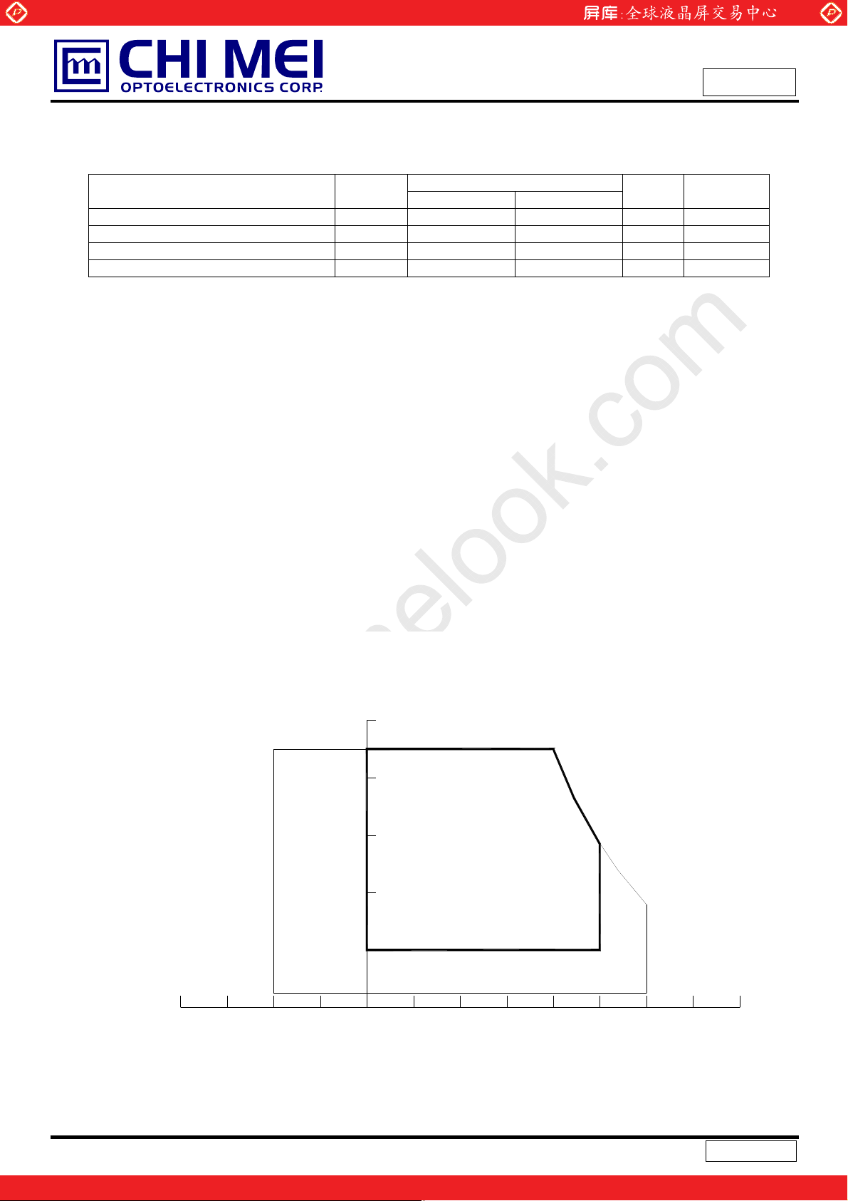
2. ABSOLUTE MAXIMUM RATINGS
2.1 ABSOLUTE RATINGS OF ENVIRONMENT
Item Symbol
Storage Temperature TST -20 +60 ºC (1)
Operating Ambient Temperature TOP 0 50 ºC (1), (2)
Shock (Non-Operating) S
Vibration (Non-Operating) V
Note (1) Temperature and relative humidity range is shown in the figure below.
(a) 90 %RH Max. (Ta Љ 40 ºC).
(b) Wet-bulb temperature should be 39 ºC Max. (Ta > 40 ºC).
(c) No condensation.
Note (2) The maximum operating temperature is based on the test condition that the surface temperature of
www.panelook.com
Issued Date: Nov. 29, 2004
Model No.: V201V2 -T03
Approval
Value
Min. Max.
- 50 G (3), (5)
NOP
- 1.0 G (4), (5)
NOP
Unit Note
display area is less than or equal to 60 ºC with LCD module alnoe in a temperature controlled chamber.
Thermal management should be considered in your product design to prevent the surface temperature
of display area from being over 60 ºC. The range of operating temperature may degrade in case of
improper thermal management in your product design.
Note (3) 11 ms, half sine wave, 1 time for ± X, ± Y, ± Z.
Note (4) 10 ~ 500 Hz, 10 min, 1 time each X, Y, Z.
Note (5) At testing Vibration and Shock, the fixture in holding the module has to be hard and rigid enough so that
the module would not be twisted or bent by the fixture.
Relative Humidity (%RH)
100
90
80
60
Operating Range
40
20
10
-40 -20 200406080
Storage Range
Temperature (ºC)
5
Version 2.1
One step solution for LCD / PDP / OLED panel application: Datasheet, inventory and accessory!
www.panelook.com
Page 6
Global LCD Panel Exchange Center
)
(1), (3)
2.2 ELECTRICAL ABSOLUTE RATINGS
2.2.1 TFT LCD MODULE
Item Symbol
Power Supply Voltage Vcc -0.3 +6.0 V
2.2.2 BACKLIGHT INVERTER UNIT
Item Symbol
Lamp Voltage V
Power Supply Voltage V
Control Signal Level
Note (1) Permanent damage to the device may occur if maximum values are exceeded. Functional operation
should be restricted to the conditions described under normal operating conditions.
www.panelook.com
Issued Date: Nov. 29, 2004
Model No.: V201V2 -T03
Value
Min. Max.
Value
Min. Max.
030V(1
Ё
Ё
-0.3 7 V
3000 V
Unit Note
Unit Note
Approval
Note (2) No moisture condensation or freezing.
Note (3) The control signals includes On/Off Control, Internal PWM Control, External PWM Control and
Internal/External PWM Selection.
6
Version 2.1
One step solution for LCD / PDP / OLED panel application: Datasheet, inventory and accessory!
www.panelook.com
Page 7
Global LCD Panel Exchange Center
www.panelook.com
Issued Date: Nov. 29, 2004
Model No.: V201V2 -T03
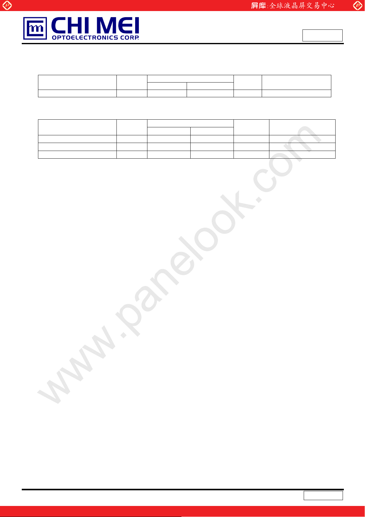
3. ELECTRICAL CHARACTERISTICS
3.1 TFT LCD MODULE Ta = 25 ± 2 ºC
Parameter Symbol
Min. Typ. Max.
Power Supply Voltage Vcc 4.5 5.0 5.5 V (1)
Ripple Voltage VRP - - 150 mV
Rush Current I
- 2.0 2.5 A (2)
RUSH
White - 0.5 0.6 A
Power Supply Current
Black - 0.4 - A
Vertical Stripe
lcc
- 0.4 0.5 A
TTL input high threshold voltage VIH 2.7 - 3.3 V
TTL input low threshold voltage VIL 0 - 0.7 V
Note (1) The module should be always operated within above ranges.
Note (2) Measurement Conditions:
Value
Unit Note
Approval
(3)
+5.0V
R1
47K
Q1 2SK 1475
FUSE
C3
1uF
Vcc
(LCD Module Input)
(High to Low)
(Control Signal)
SW
+12V
C1
1uF
VR1
R2
1K
47K
0.01uF
Q2
2SK1470
C2
Vcc rising time is 470Ps
+5V
0.9Vcc
0.1Vcc
GND
470Ps
7
Version 2.1
One step solution for LCD / PDP / OLED panel application: Datasheet, inventory and accessory!
www.panelook.com
Page 8

Global LCD Panel Exchange Center
Note (3) The specified power supply current is under the conditions at Vcc = 5 V, Ta = 25 ± 2 ºC, f
Hz, whereas a power dissipation check pattern below is displayed.
www.panelook.com
Issued Date: Nov. 29, 2004
Model No.: V201V2 -T03
Approval
= 60
v
a. White Pattern
Active Area
c. Vertical Stripe Pattern
b. Black Pattern
Active Area
R
G
G
B
R
G
B
R
B
B
B
R
R
R
G
G
G
B
B
B
R
R
Active Area
3.2 BACKLIGHT UNIT
3.2.1 CCFL (Cold Cathode Fluorescent Lamp) CHARACTERISTICS (
Parameter Symbol
Lamp Voltage VW
Lamp Current IL
Lamp Starting Voltage VS
Operating Frequency FO 40 - 70 KHz (3)
Lamp Life Time LBL 50,000 60,000 - Hrs (4)
Min. Typ. Max.
- 840 -
4.2 4.5 4.8
- - 1730
- - 1530
Value
B
G
Ta = 25 ± 2 ºC)
V
mA
V
V
B
G
RR
Unit Note
I
RMS
(1)
RMS
(2), Ta = 0 ºC
RMS
(2), Ta = 25 ºC
RMS
= 4.5mA
L
8
Version 2.1
One step solution for LCD / PDP / OLED panel application: Datasheet, inventory and accessory!
www.panelook.com
Page 9
Global LCD Panel Exchange Center
A
A
A
A A A A
A
A
A A A
3.2.2 INVERTER CHARACTERISTICS (Ta = 25 ± 2 ºC)
Parameter Symbol
Power Consumption PBL - 50 - W (5), IL = 4.5mA
Power supply Voltage VBL 18 19 20 VDC
Power supply Current IBL
Input Ripple Noise - --400 mV
V
Voltage
Oscillating Frequency FW 55 58 61 kHz
Dimming frequency FB 150 160 170 Hz
Minimum Duty Ratio D
Note (1) Lamp current is measured by utilizing high frequency current meters as shown below:
BS
MIN
www.panelook.com
Issued Date: Nov. 29, 2004
Model No.: V201V2 -T03
Approval
Value
Min. Typ. Max.
-
1650 - 3000 V
1320 - 3000 V
2.6
-
- 10 - %
Unit Note
A Non Dimming
P-P
Ta = 0 ºC Backlight Turn on
RMS
Ta = 25 ºC
RMS
VBL=18V
LCD
Module
LV (Pink,+)
LV (White,-)
Note (2) The lamp starting voltage V
up duration. Otherwise the lamp may not be turned on.
HV (Pink,+)
HV (White,+)
HV (Pink,-)
HV (White,-)
HV (Pink,+)
HV (White,+)
HV (Pink,-)
HV (White,-)
HV (Pink,+)
HV (White,+)
HV (Pink,-)
HV (White,-)
should be applied to the lamp for more than 1 second under starting
S
1
2
1
2
1
2
1
2
Inverter
1
2
1
2
Note (3) The lamp frequency may produce interference with horizontal synchronous frequency from the
display, and this may cause line flow on the display. In order to avoid interference, the lamp
frequency should be detached from the horizontal synchronous frequency and its harmonics as far
as possible.
Note (4) The life time of a lamp is defined as when the brightness is larger than 50% of its original value
and the effective discharge length is longer than 80% of its original length (Effective discharge
length is defined as an area that has equal to or more than 70% brightness compared to the
brightness at the center point.) as the time in which it continues to operate under the condition Ta
= 25 2к and I
= 4.0 ~ 5.0mA
L
RMS
.
Note (5) The power supply capacity should be higher than the total inverter power consumption P
9
Version 2.1
One step solution for LCD / PDP / OLED panel application: Datasheet, inventory and accessory!
. Since
BL
www.panelook.com
Page 10

Global LCD Panel Exchange Center
the pulse width modulation (PWM) mode was applied for backlight dimming, the driving current
changed as PWM duty on and off. The transient response of power supply should be considered
for the changing loading when inverter dimming.
3.2.3 INVERTER INTERTFACE CHARACTERISTICS
www.panelook.com
Issued Date: Nov. 29, 2004
Model No.: V201V2 -T03
Approval
Item Symbol
On/Off Control
Voltage
Internal/External
PWM Select Voltage
Internal PWM
Control Voltage
External PWM
Control Voltage
ON
V
BLON
OFF
HI
V
SEL
LO
MAX
V
V
IPWM
MIN
HI 2.0
V
V
EPWM
LO
Control Signal Rising Time Tr Ё Ё Ё 100 ms
Control Signal Falling Time Tf Ё Ё Ё 100 ms
PWM Signal Rising Time T
PWM Signal Falling Time T
Ё Ё Ё 50 us
PWMR
Ё Ё Ё 50 us
PWMF
Te st
Condition
Ё
Ё
Ё
Ё
= L
SEL
= H
SEL
Min. Typ. Max. Unit Note
2.0
Ё
5.0 V
0
2.0
Ё
Ё
0.8 V
5.0 V
0
Ё
Ё Ё
Ё
0
Ё
0
Ё
0.8 V
3.0 V minimum duty ratio
Ё
V maximum duty ratio
5.0 V duty on
0.8 V duty off
Input impedance RIN Ё 1 Ё Ё MӨ
BLON Delay Time Ton Ё 500 Ё Ё ms
BLON Off Time T
Ё 500 Ё Ё ms
off
Note (1) The SEL signal should be valid before backlight turns on by BLON signal. It is inhibited to change
the internal/external PWM selection (SEL) during backlight turn on period.
Note (2) The power sequence and control signal timing are shown as the following figure.
10
Version 2.1
One step solution for LCD / PDP / OLED panel application: Datasheet, inventory and accessory!
www.panelook.com
Page 11

Global LCD Panel Exchange Center
V
BL
www.panelook.com
Issued Date: Nov. 29, 2004
Model No.: V201V2 -T03
Approval
V
V
EPWM
V
BLON
V
SEL
IPWM
V
Toff
100%
2.0V
0.8V
2.0V
0.8V
2.0V
0.8V
3.0V
PWM
Period
Ton
Backlight on duration
Tr Tf
Ext. Dimming Function
T
T
PWMR
PWMF
Int. Dimming Function
External
PWM Duty
Minimun
Duty
0
0
0
0
0
W
External
11
Version 2.1
One step solution for LCD / PDP / OLED panel application: Datasheet, inventory and accessory!
www.panelook.com
Page 12

Global LCD Panel Exchange Center
www.panelook.com
Issued Date: Nov. 29, 2004
Model No.: V201V2 -T03
Approval
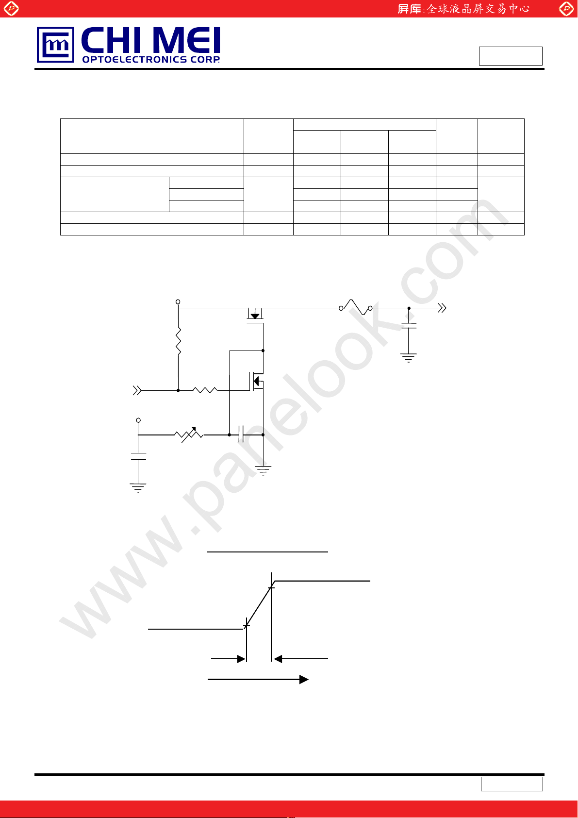
4. BLOCK DIAGRAM
4.1 TFT LCD MODULE
R0~R7
G0~G7
B0~B7
DCLK
DE
Vcc
GND
VBL
GND
SEL
E_PWM
I_PWM
BLON
(P-TWO AF7501-N2G1Z)
INPUT CONNECTOR
CN1:S12B-PH-SM3-TB(D)(LF)
FRAME BUFFER
TIMING CONTROLLER
DC/DC CONVERTER &
REFERENCE VOLTAGE
INVERTER CONNECTOR
CN8: S2B-ZR-SM3A-TF(D)(LF)
SCAN DRIVER IC
DATA DRIVER IC
CN2-CN7:SM02(12.0)B-BHS-1-TB(LF
TFT LCD PANEL
(640x3x480)
BACKLIGHT
UNIT
12
Version 2.1
One step solution for LCD / PDP / OLED panel application: Datasheet, inventory and accessory!
www.panelook.com
Page 13

Global LCD Panel Exchange Center
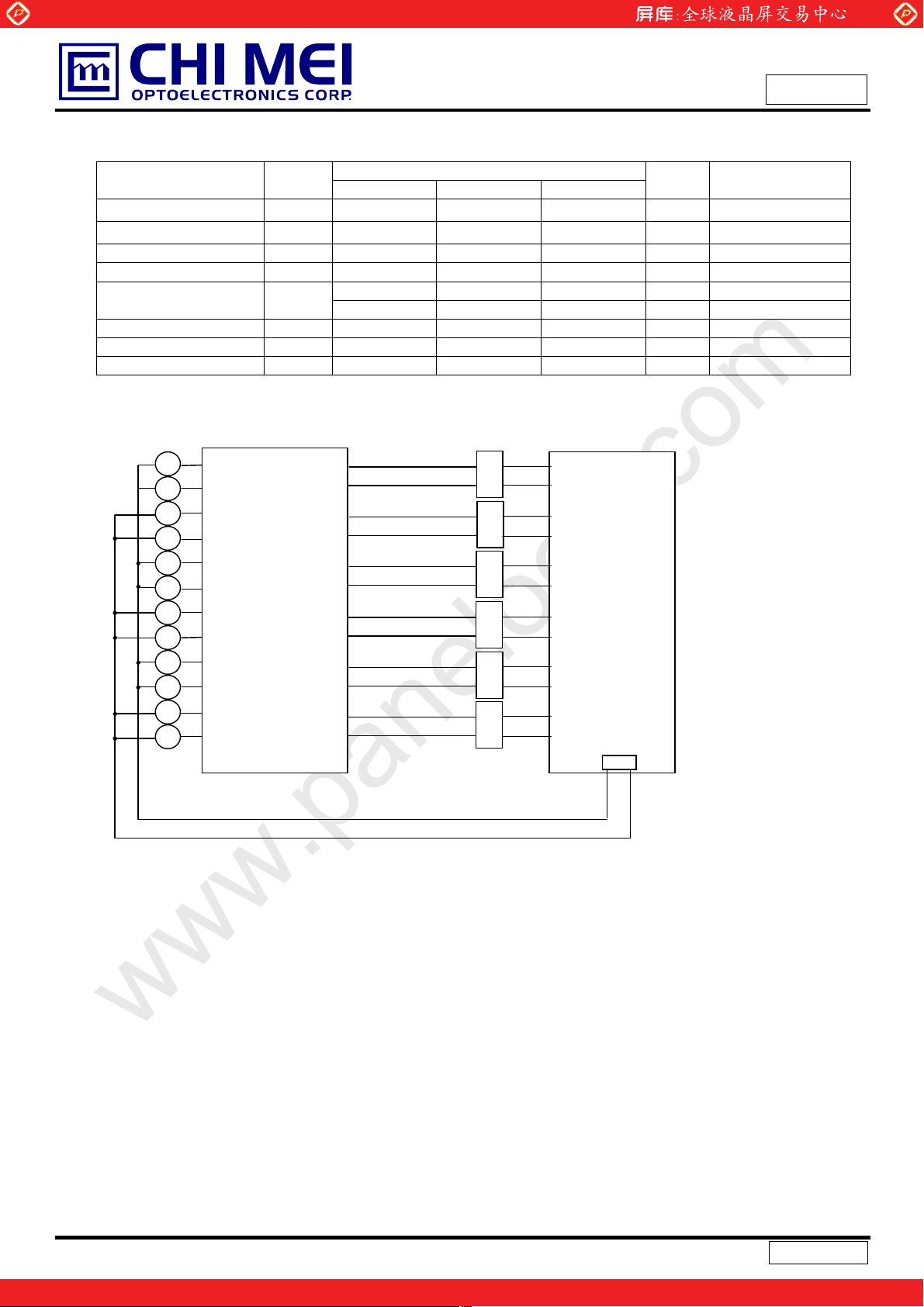
5. INTERFACE PIN CONNECTION
5.1 TFT LCD MODULE
CN1 Connector Pin Assignment
Pin Name Description
1 NC No Connection
2 NC No Connection
3 NC No Connection
4 GND Ground
5 GND Ground
6 VCC
7 VCC
8 VCC
9 VCC
10 GND Ground
11 NC
12 NC
13 GND Ground
14 DE Data Enable
15 GND Ground
16 DCLK Dot Clock
17 GND Ground
18 R7
19 R6
20 R5
21 R4
22 GND Ground
23 R3
R2 49
24
R1
25
Note (1) CN1 Connector Part No.: AF7501-N2G1Z (P-TWO) or compatible
Power Input (+5.0V)
Red Data (R7:MSB)
Red Data
www.panelook.com
Pin Name Description
26 R0 Red Data
27 GND Ground
28 G7
29 G6
30 G5
31 G4
32 GND Ground
33 G3
34 G2
35 G1
36 G0
37 GND Ground
38 B7
39 B6
40 B5
41 B4
42 GND Ground
43 B3
44 B2
45 B1
46 B0
47 GND Ground
48 GND Ground
NC No Connection
50
NC No Connection
Issued Date: Nov. 29, 2004
Model No.: V201V2 -T03
Approval
Green Data (G7:MSB)
Green Data
Blue Data (B7:MSB)
Blue Data
Note (2) NC :Reserved for internal use. Left it open.
13
Version 2.1
One step solution for LCD / PDP / OLED panel application: Datasheet, inventory and accessory!
www.panelook.com
Page 14

Global LCD Panel Exchange Center
5.2 COLOR DATA INPUT ASSIGNMENT
The brightness of each primary color (red, green and blue) is based on the 8-bit gray scale data input for
the color. The higher the binary input, the brighter the color. The table below provides the assignment of color
versus data input.
Color
R7 R6 R5 R4 R3 R2 R1 R0 G7 G6 G5 G4 G3 G2 G1 G0 B7 B6 B5 B4 B3 B2 B1 B0
Basic
Colors
Gray
Scale
Of
Red
Black
Red
Green
Blue
Cyan
Magenta
Yellow
White
Red(0) / Dark
Red(1)
Red(2)
:
:
Red(253)
Red(254)
Red(255)
0
0
1
1
0
0
0
0
0
0
1
1
1
1
1
1
0
0
0
0
0
0
:
:
:
:
1
1
1
1
1
1
www.panelook.com
Issued Date: Nov. 29, 2004
Model No.: V201V2 -T03
Approval
Data Signal
Red Green Blue
0
0
0
1
0
0
0
1
1
1
0
0
0
1
1
1
0
0
0
0
0
0
0
0
0
0
0
0
0
1
1
1
1
1
0
0
0
0
0
0
0
0
0
0
0
0
1
1
1
1
1
1
1
0
0
0
0
0
0
0
0
0
0
0
0
0
0
0
0
0
1
1
1
1
1
1
1
1
1
1
1
1
0
0
0
0
0
0
0
1
1
1
1
1
1
1
1
1
1
1
1
1
1
1
1
1
1
1
1
1
1
1
1
0
0
0
0
0
0
0
0
0
0
0
0
0
0
0
0
1
0
0
0
0
0
0
0
0
0
0
1
0
0
0
0
0
0
0
0
:
:
:
:
:
:
:
:
:
:
:
:
:
:
:
:
:
:
:
:
:
:
:
:
:
:
1
1
1
0
1
0
0
0
0
0
0
0
1
1
1
1
0
0
0
0
0
0
0
0
1
1
1
1
1
0
0
0
0
0
0
0
0
1
0
1
0
1
1
0
0
0
0
0
0
0
0
1
1
1
0
1
0
0
0
:
:
0
0
0
0
0
0
0
0
0
0
0
0
0
0
0
0
0
0
0
0
0
0
0
1
1
1
1
1
1
1
1
1
1
1
1
1
1
1
1
1
1
1
1
1
0
0
0
0
0
0
0
1
1
1
1
1
1
1
0
0
0
0
0
0
0
0
0
0
0
0
0
0
0
0
0
0
0
0
0
:
:
:
:
:
:
:
:
:
:
:
:
:
:
:
:
0
0
0
0
0
0
0
0
0
0
0
0
0
0
0
0
0
0
0
0
0
Green(0) / Dark
Gray
Scale
Of
Green
Gray
Scale
Of
Blue
Note (1) 0: Low Level Voltage, 1: High Level Voltage
Green(1)
Green(2)
:
:
Green(253)
Green(254)
Green(255)
Blue(0) / Dark
Blue(1)
Blue(2)
:
:
Blue(253)
Blue(254)
Blue(255)
0
0
0
0
0
0
0
0
0
0
0
0
0
0
0
0
0
0
0
0
0
:
:
:
:
:
:
:
:
:
:
:
:
:
:
0
0
0
0
0
0
0
0
0
0
0
0
0
0
0
0
0
0
0
0
0
0
0
0
0
0
0
0
0
0
0
0
0
0
0
0
0
0
0
0
0
0
:
:
:
:
:
:
:
:
:
:
:
:
:
:
0
0
0
0
0
0
0
0
0
0
0
0
0
0
0
0
0
0
0
0
0
0
0
0
0
0
0
0
0
0
0
0
0
0
0
0
0
1
0
0
0
0
0
0
0
0
0
0
0
0
0
0
0
0
0
0
0
0
0
0
1
:
:
:
:
:
:
:
:
:
:
:
:
:
:
0
1
1
1
1
1
1
0
1
1
1
1
1
1
0
1
1
1
1
1
1
0
0
0
0
0
0
0
0
0
0
0
0
0
0
0
0
0
0
0
0
0
:
:
:
:
:
:
:
:
:
:
:
:
:
:
0
0
0
0
0
0
0
0
0
0
0
0
0
0
0
0
0
0
0
0
0
:
:
:
:
1
0
1
0
0
0
0
0
0
0
0
0
0
0
0
:
:
1
1
1
0
1
1
0
0
0
:
:
0
0
0
0
:
:
:
:
0
0
0
0
0
0
0
0
0
0
0
0
:
:
:
:
1
1
1
1
1
1
0
0
0
:
:
:
:
:
:
0
0
0
0
0
0
0
0
0
0
0
0
:
:
:
:
:
:
1
1
1
1
1
1
0
0
0
0
0
0
0
:
:
:
:
:
:
0
0
0
0
0
0
0
0
0
0
0
0
0
0
1
0
1
0
:
:
:
:
:
:
1
0
1
1
1
0
1
1
1
14
Version 2.1
One step solution for LCD / PDP / OLED panel application: Datasheet, inventory and accessory!
www.panelook.com
Page 15
Global LCD Panel Exchange Center
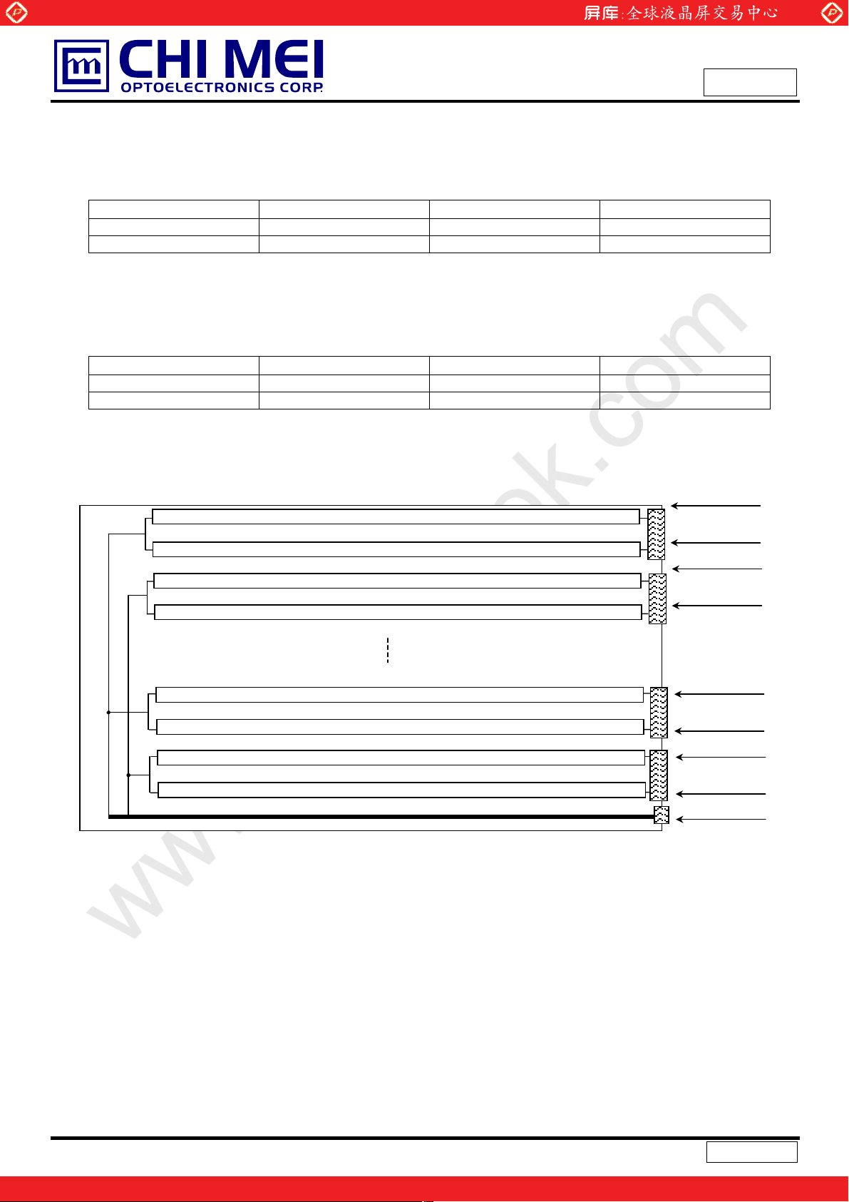
5.3 BACKLIGHT UNIT
The pin configuration for the housing and leader wire is shown in the table below.
Pin No. Symbol
1 HV High Voltage Pink
2 HV High Voltage White
Note (1) The backlight interface housing for high voltage side is a model BHR-04VS-1, manufactured by JST.
The mating header on inverter part number is SM02(12.0)B-BHS-1-TB(LF)(JST).
Pin Signal name Feature
1 LV Low Voltage(+) Pink
2 LV Low Voltage(-) White
Note (2) The backlight interface housing and return cable for low voltage side is a model ZHR-2, manufactured
www.panelook.com
Issued Date: Nov. 29, 2004
Model No.: V201V2 -T03
Approval
CN2-CN7(Housing): BHR-04VS-1
Description Wire Color
CN8(Housing): ZHR-2 or equivalent
Wire Color
by JST or equivalent. The mating header on inverter part number is S2B-ZR-SM3A-TF(D)(LF) or
equivalent.
1 HV(Pink,+)
2 HV(White,+)
1 HV(Pink,-)
2 HV(White,-)
1 HV(Pink,+)
2 HV(White,+)
1 HV(Pink,-)
2 HV(White,-)
RETURN CABLE
LV (Pink,+)
LV (White,-)
15
Version 2.1
One step solution for LCD / PDP / OLED panel application: Datasheet, inventory and accessory!
www.panelook.com
Page 16

Global LCD Panel Exchange Center
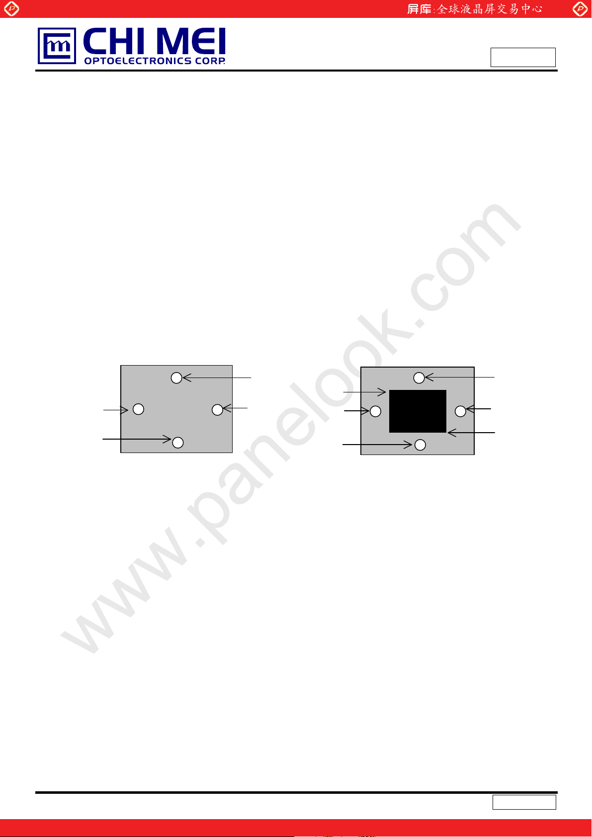
5.4 INVERTER UNIT
CN1(Header): S12B-PH-SM3-TB(D)(LF)(JST) or equivalent
Pin No. Symbol Description
1
2
3
4
5
6
7
8
9 SEL
10 E_PWM
11 I_PWM
12 BLON Backlight on/off control
CN2-CN7(Header):SM02(12.0)B-BHS-1-TB (LF)(JST)
Pin No. Symbol Description
1 CCFL HOT CCFL high voltage
2 CCFL HOT CCFL high voltage
VBL +19V Power input
GND Ground
Internal/external PWM selection
High : external dimming
Low : internal dimming
External PWM control signal
E_PWM should be connected to low when internal PWM was selected (SEL =
low).
Internal PWM control signal
I_PWM should be connected to ground when external PWM was selected (SEL =
high).
www.panelook.com
Issued Date: Nov. 29, 2004
Model No.: V201V2 -T03
Approval
CN8(Header):S2B-ZR-SM3A-TF(D)(LF)(JST) or equivalent
Pin No. Symbol Description
1 CCFL COLD CCFL low voltage (+)
2 CCFL COLD CCFL low voltage (-)
Note (1) Floating of any control signal is not allowed.
16
Version 2.1
One step solution for LCD / PDP / OLED panel application: Datasheet, inventory and accessory!
www.panelook.com
Page 17

Global LCD Panel Exchange Center
6. INTERFACE TIMING
6.1 INPUT SIGNAL TIMING SPECIFICATIONS
The input signal timing specifications are shown as the following table and timing diagram.
Signal Item Symbol Min. Typ. Max. Unit Note
Clock Frequency 1/Tc 20 25.175 30 MHZ -
Frame Rate Fr 47 60 63 Hz -
Vertical Active Display Term
Horizontal Active Display Term
Input data Term
DE Term
Note: Since this module is operated in DE only mode, Hsync and Vsync input signals should be set to low
Total Tv 500 525 550 Th Tv=Tvd+Tvb
Display Tvd 480 480 480 Th Blank Tvb 20 45 70 Th Total Th 750 800 850 Tc Th=Thd+Thb
Display Thd 640 640 640 Tc Blank Thb 110 160 210 Tc Setup time TS 15 -- -- ns
Hold time T
Setup time TSDE
Hold time T
www.panelook.com
H 10 -- -- ns
15
HDE
10
Issued Date: Nov. 29, 2004
Model No.: V201V2 -T03
Approval
-- -- ns
-- -- ns
logic level or ground. Otherwise, this module would operate abnormally.
INPUT SIGNAL TIMING DIAGRAM
Tvd
DE
Th
DCLK
Tc
Thb
DE
DATA
v
T
Thd
Valid display data (640 cks)
Tvb
DCLK
DE
50%
TSDE
80%
TS
80%
TH
50%
50%
THDE
80%
DATA
20%20%
17
Version 2.1
One step solution for LCD / PDP / OLED panel application: Datasheet, inventory and accessory!
80%
www.panelook.com
Page 18

Global LCD Panel Exchange Center
Љ
Љ
Љ
Љ
Љ
6.2 POWER ON/OFF SEQUENCE
To prevent a latch-up or DC operation of LCD module, the power on/off sequence should be as the
diagram below.
www.panelook.com
Issued Date: Nov. 29, 2004
Model No.: V201V2 -T03
Approval
Power Supply
V
0ЉT1Љ10ms
0
0
500ms
CC
0V
2
50ms
T
3
50ms
T
4
T
Signals
0V
Backlight (Recommended)
100msЉT5
100msЉT6
0.9 VCC
CC
0.1V
Power On
CC
0.9 V
cc
0.1V
3 T1
T
T
2
T4
VALID
Power Off
50%
5
T
50%
T
6
Power ON/OFF Sequence
Note (1) The supply voltage of the external system for the module input should follow the definition of Vcc.
Note (2) Apply the lamp voltage within the LCD operation range. When the backlight turns on before the LCD
operation or the LCD turns off before the backlight turns off, the display may momentarily become abnormal
screen.
Note (3) In case of Vcc is in
Note (4) T4 should be measured after the module has been fully discharged between power off and on period.
Note (5) Interface signal shall not be kept at high impedance when the power is on.
off level, please keep the level of input signals on the low or high impedance.
18
Version 2.1
One step solution for LCD / PDP / OLED panel application: Datasheet, inventory and accessory!
www.panelook.com
Page 19

Global LCD Panel Exchange Center
7. OPTICAL CHARACTERISTICS
7.1 TEST CONDITIONS
Item Symbol Value Unit
Ambient Temperature Ta
Ambient Humidity Ha
Supply Voltage VCC 5.0 V
Input Signal According to typical value in "3. ELECTRICAL CHARACTERISTICS"
Lamp Current IL
Oscillating Frequency (Inverter) FW
7.2 OPTICAL SPECIFICATIONS
The relative measurement methods of optical characteristics are shown in 7.2. The following items should be
measured under the test conditions described in 7.1 and stable environment shown in Note (6).
Item Symbol Condition Min. Typ. Max. Unit Note
Contrast Ratio CR 800 1000 - - Note(2)
Response Time
Center Luminance of White L
White Variation
Cross Talk CT - - 4 % Note(5)
Red
Green
Color
Chromaticity
Viewing
Angle
Blue
White
Color Gamut
Horizontal
Verti ca l
www.panelook.com
Issued Date: Nov. 29, 2004
Model No.: V201V2 -T03
o
25r2
50r10
4.5r0.5
58r3
Gray to
gray
average
C
GW
T
=0q, TY =0q
Rx 0.622 0.652 0.682 Ry 0.302
Gx 0.243
Gy 0.568
Bx 0.112
By 0.038
Wx 0.251 0.281 0.311 Wy
Tx+
T
-
x
TY+
T
-
Y
x
Viewing Normal Angle
CRt20
8 12 Note(3)
400 500 - cd/m2Note(4)
- - 1.25 - Note(7)
0.332
0.273
0.598
0.142
0.068
0.258 0.288 0.318 72 75 - %
80 88 80 88 80 88 80 88 -
0.362 -
0.303 -
0.628 -
0.172 -
0.098 -
C
%RH
mA
KHz
Deg. Note(1)
Approval
Color
Chromat
icity
NTSC
19
Version 2.1
One step solution for LCD / PDP / OLED panel application: Datasheet, inventory and accessory!
www.panelook.com
Page 20

Global LCD Panel Exchange Center
Note (1) Definition of Viewing Angle (Tx, Ty):
Viewing angles are measured by Eldim EZ-Contrast 160R
www.panelook.com
Issued Date: Nov. 29, 2004
Model No.: V201V2 -T03
Approval
TX- = 90º
x-
6 o’clock
T
y- = 90º
y-
Note (2) Definition of Contrast Ratio (CR):
The contrast ratio can be calculated by the following expression.
Contrast Ratio (CR) = L255 / L0
Normal
Tx = Ty = 0º
yTy-
T
Tx
Tx
12 o’clock direction
y+
T
y+ = 90º
x+
T
X+ = 90º
L255: Luminance of gray level 255
L 0: Luminance of gray level 0
CR = CR (5)
CR (X) is corresponding to the Contrast Ratio of the point X at the figure in Note (7).
Note (3) Definition of Gray to Gray Switching Time:
100%
90%
Optical
Response
10%
0%
Gray to gray
switching time
Gray to gray
switching time
Time
20
Version 2.1
One step solution for LCD / PDP / OLED panel application: Datasheet, inventory and accessory!
www.panelook.com
Page 21
Global LCD Panel Exchange Center
A
A
The driving signal means the signal of gray level 0, 63, 127,191, 255.
Gray to gray average time means the average switching time of gray level 0, 63,127,191, 255
to each other.
www.panelook.com
Issued Date: Nov. 29, 2004
Model No.: V201V2 -T03
Approval
Note (4) Definition of Luminance of White (LC, L
Measure the luminance of gray level 255 at center point and 5 points
LC = L (5)
L
= [L (1)+ L (2)+ L (3)+ L (4)+ L (5)] / 5
AVE
L (x) is corresponding to the luminance of the point X at the figure in Note (7).
Note (5) Definition of Cross Talk (CT):
CT = | Y
– YA | / YA u 100 (%)
B
Where:
Y
= Luminance of measured location without gray level 0 pattern (cd/m2)
A
Y
= Luminance of measured location with gray level 0 pattern (cd/m2)
B
(0, 0)
ctive Area
Y
(D/8,W/2)
A, L
Gray 128
Y
(D/2,7W/8)
A, D
Y
A, U
Y
A, R
(D,W)
):
AVE
(D/2,W/8)
(7D/8,W/2)
(D/4,W/4)
Y
(D/8,W/2)
B, L
Y
(D/2,7W/8)
B, D
(0, 0)
ctive Area
Gray 0
Gray 0
Gray 128
Y
B, U
Y
B, R
(3D/4,3W/4)
(D,W)
(D/2,W/8)
(7D/8,W/2)
21
Version 2.1
One step solution for LCD / PDP / OLED panel application: Datasheet, inventory and accessory!
www.panelook.com
Page 22

Global LCD Panel Exchange Center
Note (6) Measurement Setup:
The LCD module should be stabilized at given temperature for 1 hour to avoid abrupt temperature
change during measuring. In order to stabilize the luminance, the measurement should be
executed after lighting Backlight for 1 hour in a windless room.
LCD Module
www.panelook.com
Issued Date: Nov. 29, 2004
Model No.: V201V2 -T03
Approval
Note (7) Definition of White Variation (GW):
Measure the luminance of gray level 255 at 5 points
GW = Maximum [L (1), L (2), L (3), L (4), L (5)] / Minimum [L (1), L (2), L (3), L (4), L (5)]
LCD Panel
Center of the Screen
Display Color Analyzer
(Minolta CA210)
Light Shield Room
(Ambient Luminance < 2 lux)
Horizontal Line
D
3D/4D/2D/4
Vertical Line
W
W/4
W/2
3W/4
5
Active Area
21
X
: Test Point
X=1 to 5
43
22
Version 2.1
One step solution for LCD / PDP / OLED panel application: Datasheet, inventory and accessory!
www.panelook.com
Page 23

Global LCD Panel Exchange Center
8. PACKAGING
8.1 PACKING SPECIFICATIONS
(1) 5 TV LCD modules / 1 Box
(2) Box dimensions : 535(L) X 357 (W) X 460 (H)
(3) Weight : approximately 13Kg ( 5 modules per box)
8.2 PACKING METHOD
Figures 9-1 and 9-2 are the packing method
LCD TV Module
www.panelook.com
Issued Date: Nov. 29, 2004
Model No.: V201V2 -T03
Approval
Anti-Static Bag
PP Foam(Bottom)
Carton
Carton dimensions:535(L)x357(W)x460(H)mm
Weight
Drier
Figure.9-1 packing method
: Approx. 13Kg(5modules per 1 carton)
Carton Label
23
Version 2.1
One step solution for LCD / PDP / OLED panel application: Datasheet, inventory and accessory!
www.panelook.com
Page 24

Global LCD Panel Exchange Center
PE Sheet
www.panelook.com
Issued Date: Nov. 29, 2004
Model No.: V201V2 -T03
Approval
Corner Protector:L1350*50mm*50mm
Pallet:L1100*W1100*H135mm
Bottom Cap:L1100*W1100*H120mm
Pallet Stack:L1100*W1100*H1515mm
Gross:260kg
Film
Carton Label
PP Belt
Figure. 9-2 Packing method
24
Version 2.1
One step solution for LCD / PDP / OLED panel application: Datasheet, inventory and accessory!
www.panelook.com
Page 25

Global LCD Panel Exchange Center
9. DEFINITION OF LABELS
9.1 CMO MODULE LABEL
The barcode nameplate is pasted on each module as illustration, and its definitions are as following explanation.
www.panelook.com
Issued Date: Nov. 29, 2004
Model No.: V201V2 -T03
Approval
CHI MEI
OPTOELECTRONICS
(a) Model Name: V201V2 -T03
(b) Revision: Rev. XX, for example: A0, A1… B1, B2… or C1, C2…etc.
(c) Serial ID: X X X X X X X Y M D L N N N N
V201V2 -T03 Rev. XX
X X X X X X X Y M D L N N N N
Serial No.
Product Line
Year, Month, Date
CMO Internal Use
CMO Internal Use
Revision
E207943
MADE IN TAIWAN
Serial ID includes the information as below:
(a) Manufactured Date: Year: 0~9, for 2000~2009
Month: 1~9, A~C, for Jan. ~ Dec.
Day: 1~9, A~Y, for 1
(b) Revision Code: Cover all the change
(c) Serial No.: Manufacturing sequence of product
(d) Product Line: 1 -> Line1, 2 -> Line 2, …etc.
CMO Internal Use
st
to 31st, exclude I ,O, and U.
25
Version 2.1
One step solution for LCD / PDP / OLED panel application: Datasheet, inventory and accessory!
www.panelook.com
Page 26

Global LCD Panel Exchange Center
www.panelook.com
Issued Date: Nov. 29, 2004
Model No.: V201V2 -T03
Approval
10. PRECAUTIONS
10.1 ASSEMBLY AND HANDLING PRECAUTIONS
(1) Do not apply rough force such as bending or twisting to the module during assembly.
(2) It is recommended to assemble or to install a module into the user’s system in clean working areas.
The dust and oil may cause electrical short or worsen the polarizer.
(3) Do not apply pressure or impulse to the module to prevent the damage of LCD panel and Backlight.
(4) Always follow the correct power-on sequence when the LCD module is turned on. This can prevent the
damage and latch-up of the CMOS LSI chips.
(5) Do not plug in or pull out the I/F connector while the module is in operation.
(6) Do not disassemble the module.
(7) Use a soft dry cloth without chemicals for cleaning, because the surface of polarizer is very soft and
easily scratched.
(8) Moisture can easily penetrate into LCD module and may cause the damage during operation.
(9) High temperature or humidity may deteriorate the performance of LCD module. Please store LCD
modules in the specified storage conditions.
(10) When ambient temperature is lower than 10ºC, the display quality might be reduced. For example, the
response time will become slow, and the starting voltage of CCFL will be higher than that of room
temperature.
10.2 SAFETY PRECAUTIONS
(1) The startup voltage of a Backlight is approximately 1000 Volts. It may cause an electrical shock while
assembling with the inverter. Do not disassemble the module or insert anything into the Backlight unit.
(2) If the liquid crystal material leaks from the panel, it should be kept away from the eyes or mouth. In
case of contact with hands, skin or clothes, it has to be washed away thoroughly with soap.
(3) After the module’s end of life, it is not harmful in case of normal operation and storage.
10.3 SAFETY REGULATION
(1) V201V2 is certified with Safety Regulation UL6500. File E240708, Volume 1.
(2) V201V2 is certified with Safety Regulation IEC 60065. Ref. Certif. No: JPTUV-007772.
26
Version 2.1
One step solution for LCD / PDP / OLED panel application: Datasheet, inventory and accessory!
www.panelook.com
Page 27
Global LCD Panel Exchange Center
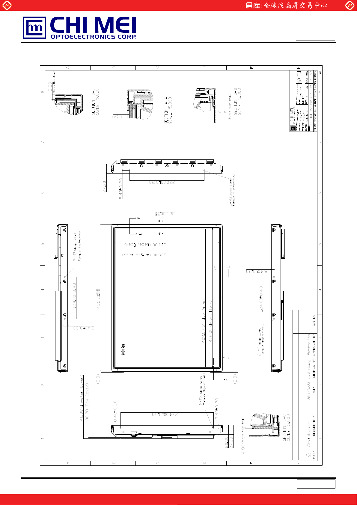
11.MECHANICAL CHARACTERISTICS
www.panelook.com
Issued Date: Nov. 29, 2004
Model No.: V201V2 -T03
Approval
奇美電子股份有限公司
27
Version 2.1
One step solution for LCD / PDP / OLED panel application: Datasheet, inventory and accessory!
www.panelook.com
Page 28

Global LCD Panel Exchange Center
www.panelook.com
Issued Date: Nov. 29, 2004
Model No.: V201V2 -T03
Approval
奇美電子股份有限公司
28
Version 2.1
One step solution for LCD / PDP / OLED panel application: Datasheet, inventory and accessory!
www.panelook.com
 Loading...