

Page 1
Global LCD Panel Exchange Center
www.panelook.com
One step solution for LCD / PDP / OLED panel application: Datasheet, inventory and accessory!
www.panelook.com
Customer:
MODEL NO.: V185B1
PRODUCT SPECIFICATION
Tentative Specification
Preliminary Specification
Approval Specification
SUFFIX: L03
APPROVED BY SIGNATURE
Name / Title
Note
Please return 1 copy for your confirmation with your
signature and comments.
Approved By Checked By Prepared By
Chao-Chun Chung
Roger Huang
Kimi Lin
Version 2.2 1 D a t e
The copyright belongs to CHIMEI Innolux. Any unauthorized use is prohibited
28 O c t 20 10
Page 2
Global LCD Panel Exchange Center
www.panelook.com
One step solution for LCD / PDP / OLED panel application: Datasheet, inventory and accessory!
www.panelook.com
PRODUCT SPECIFICATION
CONTENTS
1. GENERAL DESCRIPTION ......................................................................................................................................5
1.1 OVERVIEW....................................................................................................................................................5
1.2 FEATURES ....................................................................................................................................................5
1.3 APPLICATION................................................................................................................................................5
1.4 GENERAL SPECIFICATIONS ........................................................................................................................5
1.5 MECHANICAL SPECIFICATIONS ..................................................................................................................6
2. ABSOLUTE MAXIMUM RATINGS ...........................................................................................................................6
2.1 ABSOLUTE RATINGS OF ENVIRONMENT....................................................................................................6
2.2 PACKAGE STORAGE....................................................................................................................................7
2.3 ELECTRICAL ABSOLUTE RATINGS..............................................................................................................7
2.3.1 TFT LCD MODULE...............................................................................................................................7
2.3.2 BACKLIGHT UNIT................................................................................................................................7
3. ELECTRICAL CHARACTERISTICS ........................................................................................................................7
3.1 TFT LCD MODULE.........................................................................................................................................8
3.2 BACKLIGHT CONNECTOR PIN CONFIGURATION .....................................................................................10
3.2.1 LAMP SPECIFICATION......................................................................................................................10
4. BLOCK DIAGRAM OF INTERFACE......................................................................................................................12
4.1 TFT LCD MODULE.......................................................................................................................................12
5. INPUT TERMINAL PIN ASSIGNMENT ..................................................................................................................13
5.1 TFT LCD Module Input .................................................................................................................................13
5.2 BACKLIGHT UNIT........................................................................................................................................14
5.3 BLOCK DIAGRAM OF INTERFACE .............................................................................................................15
5.4 LVDS INTERFACE.......................................................................................................................................16
5.5 COLOR DATA INPUT ASSIGNMENT............................................................................................................17
6. INTERFACE TIMING.............................................................................................................................................18
6.1 INPUT SIGNAL TIMING SPECIFICATIONS..................................................................................................18
6.2 POWER ON/OFF SEQUENCE.....................................................................................................................20
7. OPTICAL CHARACTERISTICS.............................................................................................................................21
7.1 TEST CONDITIONS.....................................................................................................................................21
7.2 OPTICAL SPECIFICATIONS ........................................................................................................................22
Version 2.2 2 D a t e
The copyright belongs to CHIMEI Innolux. Any unauthorized use is prohibited
28 O c t 20 10
Page 3

Global LCD Panel Exchange Center
www.panelook.com
One step solution for LCD / PDP / OLED panel application: Datasheet, inventory and accessory!
www.panelook.com
PRODUCT SPECIFICATION
8. PRECAUTIONS....................................................................................................................................................26
8.1 ASSEMBLY AND HANDLING PRECAUTIONS .............................................................................................26
8.2 SAFETY PRECAUTIONS.............................................................................................................................26
9. DEFINITION OF LABELS......................................................................................................................................27
9.1 CMI MODULE LABEL...................................................................................................................................27
10. PACKAGING.......................................................................................................................................................28
10.1 PACKAGING SPECIFICATIONS.................................................................................................................28
10.2 PACKAGING METHOD..............................................................................................................................28
11. MECHANICAL CHARACTERISTIC......................................................................................................................28
Version 2.2 3 D a t e
The copyright belongs to CHIMEI Innolux. Any unauthorized use is prohibited
28 O c t 20 10
Page 4
Global LCD Panel Exchange Center
www.panelook.com
One step solution for LCD / PDP / OLED panel application: Datasheet, inventory and accessory!
www.panelook.com
Version Date Page(New) Section Description
Ver 2.0
Ver 2.1
Ver 2.2
Apr.19, 10’
Jun.14, 10’
Oct,28, 10’
Page 5
Page 6
All
PRODUCT SPECIFICATION
REVISION HISTORY
All
OVERVIEW
Page 6
V185B1-L03 Approval specification was first issued.
Model name change from V185B1-L01 to V185B1-L03
Modify 1.5 MECHANICAL SPECIFICATIONS
Weight Typ. From 1965g to 1950g & Max. From 2000g to
2030g
Version 2.2 4 D a t e
The copyright belongs to CHIMEI Innolux. Any unauthorized use is prohibited
28 O c t 20 10
Page 5
Global LCD Panel Exchange Center
www.panelook.com
One step solution for LCD / PDP / OLED panel application: Datasheet, inventory and accessory!
www.panelook.com
1. GENERAL DESCRIPTION
1.1 OVERVIEW
V185B1-L03 is an 18.5” TFT Liquid Crystal Display module with 2-CCFL Backlight unit and 1ch-LVDS interface.
This module supports 1366 x 768 WXGA TV format and can display 16.7M colors. The inverter module for
backlight isn’t built-in.
1.2 FEATURES
High brightness (300 nits)
High contrast ratio (1000:1)
Fast response time (5ms)
High color saturation (NTSC 72%)
HDTV (1366 x 768 pixels) resolution, true HDTV format
DE (Data Enable) only mode
PRODUCT SPECIFICATION
LVDS (Low Voltage Differential Signaling) interface
RoHs compliance
1.3 APPLICATION
Standard Living Room TVs
Public Display Application
Home Theater Application
MFM Application
1.4 GENERAL SPECIFICATIONS
Item Specification Unit Note
Active Area 409.8 (H) × 230.4(V) (18.5” diagonal) mm
Bezel Opening Area 413.4(H) x 234 (V) mm
Driver Element a-Si TFT active matrix - -
Pixel Number 1366 x R.G.B. x 768 pixel -
Pixel Pitch(Sub Pixel) 0.3 (H) x 0.3 (V) mm -
Pixel Arrangement RGB vertical stripe - -
(1)
Power consumption 13.64 Watt (2)
Display Colors 16.7M color
Display Operation Mode Normally White - -
Surface Treatment AG type, 3H hard coating, Haze 25 - -
Note (1) Please refer to the attached drawings for more information of front and back outline dimensions.
Note (2) Please refer to sec. 3.1 & 3.2 in this document for more information of power consumption.
Version 2.2 5 D a t e
The copyright belongs to CHIMEI Innolux. Any unauthorized use is prohibited
28 O c t 20 10
-
Page 6
Global LCD Panel Exchange Center
www.panelook.com
One step solution for LCD / PDP / OLED panel application: Datasheet, inventory and accessory!
www.panelook.com
1.5 MECHANICAL SPECIFICATIONS
Item Min. Typ. Max. Unit Note
Horizontal (H) 429.87 430.37 430.87 mm
PRODUCT SPECIFICATION
Module Size
Note (1) Please refer to the attached drawings for more information of front and back outline dimensions.
Vertical (V) 254.1 254.6 255.1 mm
Depth (D) 15.75 16.25 16.75 mm
Weight - 1950 2030 g -
2. ABSOLUTE MAXIMUM RATINGS
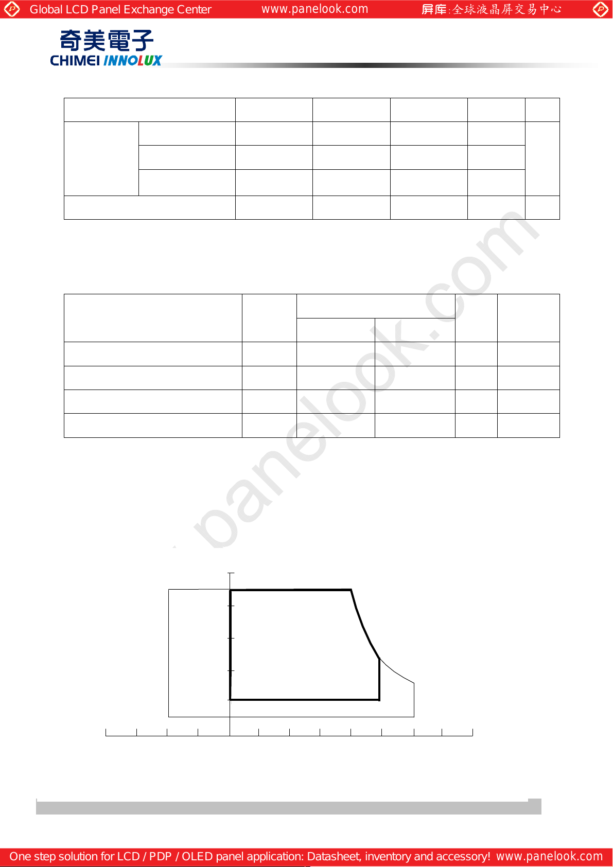
2.1 ABSOLUTE RATINGS OF ENVIRONMENT
Value
Item Symbol
Min. Max.
Storage Temperature TST -20 +60 ºC (1)
Operating Ambient Temperature TOP 0 50 ºC (1), (2)
Shock (Non-Operating) SNOP - 50 G (3), (5)
Vibration (Non-Operating) VNOP - 1.5 G (4), (5)
Note (1) Temperature and relative humidity range is shown in the figure below.
Unit Note
(1)
(a) 90 %RH Max. (Ta 40 ºC).
(b) Wet-bulb temperature should be 39 ºC Max. (Ta > 40 ºC).
(c) No condensation.
Note (2) The temperature of panel display surface area should be 0 ºC Min. and 60 ºC Max.
Relative Humidity (%RH)
100
90
80
60
40
20
10
Temperature (C)
Operating Range
Storage Range
80 60 -20 40 0 20 -40
Version 2.2 6 D a t e
The copyright belongs to CHIMEI Innolux. Any unauthorized use is prohibited
28 O c t 20 10
Page 7
Global LCD Panel Exchange Center
www.panelook.com
One step solution for LCD / PDP / OLED panel application: Datasheet, inventory and accessory!
www.panelook.com
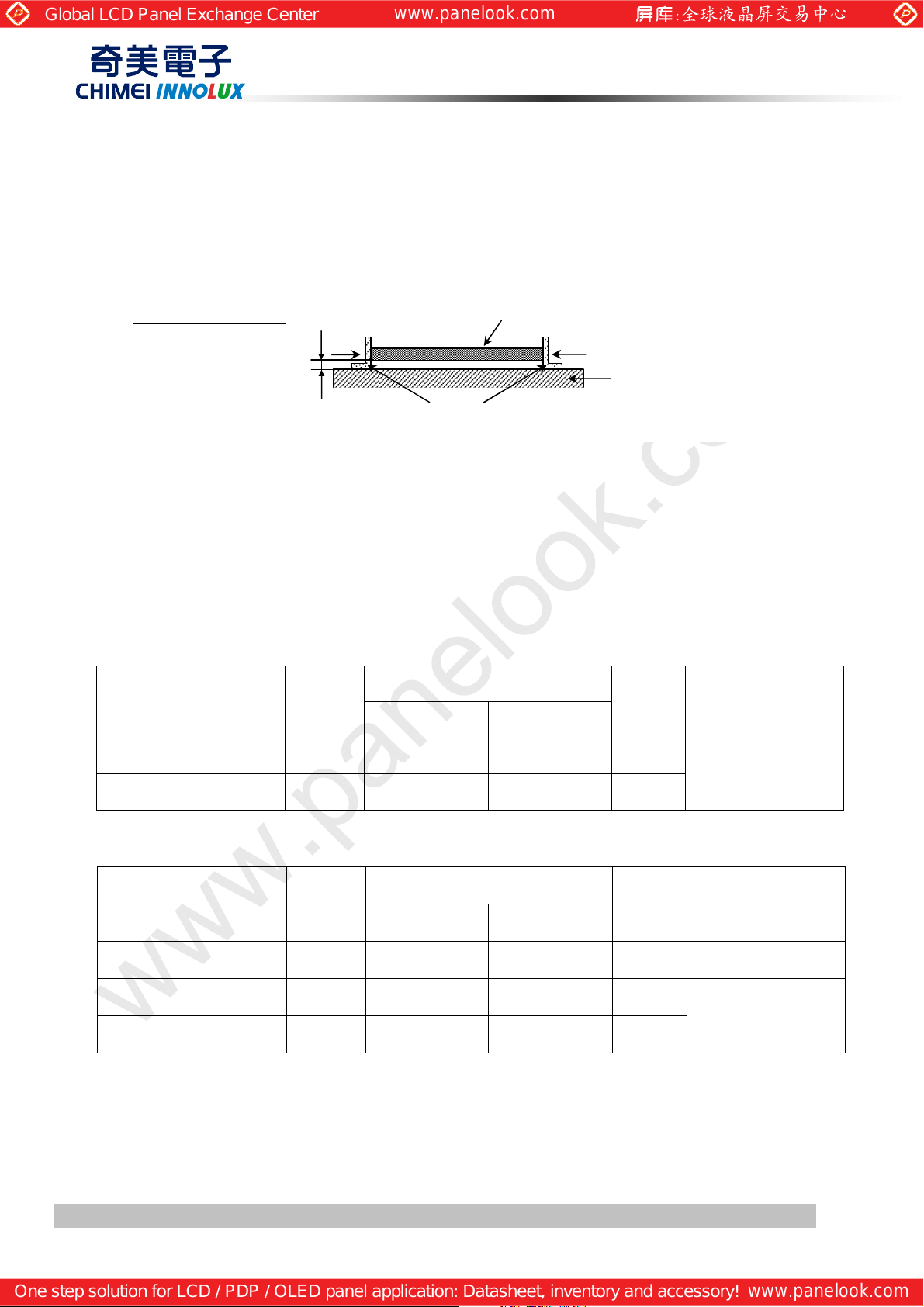
Bracket
At Room Temperature
Note (3) 50G,11ms, half sine wave, 1 time for ± X, ± Y, ± Z.
Note (4) 10 ~ 300 Hz, 10min/cycle, 3 cycles each X, Y, Z.
Note (5) At testing Vibration and Shock, the fixture in holding the module has to be hard and rigid enough so
that the module would not be twisted or bent by the fixture.
The fixing condition is shown as below:
PRODUCT SPECIFICATION
LCD Module
Side Mount Fixing Screw
Gap=3~5mm
Side Mount Fixing Screw
Stage
2.2 PACKAGE STORAGE
When storing modules as spares for a long time, the following precaution is necessary.
(a) Do not leave the module in high temperature, and high humidity for a long time, It is highly recommended to
store the module with temperature from 0 to 35 at normal humidity without condensation.
(b) The module shall be stored in dark place. Do not store the TFT-LCD module in direct sunlight or fluorescent
light.
2.3 ELECTRICAL ABSOLUTE RATINGS
2.3.1 TFT LCD MODULE
Value
Item Symbol
Min. Max.
Power Supply Voltage VCC -0.3 +6.0 V
Logic Input Voltage VIN -0.3 +2.7 V
Unit Note
(1)
2.3.2 BACKLIGHT UNIT
Value
Item Symbol
Min. Max.
Lamp Voltage VW
Lamp Current IL 2.0 8.0 mA
Lamp Frequency FL 40 80 KHz
Note (1) Permanent damage to the device may occur if maximum values are exceeded. Function operation
should be restricted to the conditions described under Normal Operating Conditions.
Note (2) Specified values are for lamp (Refer to 3.2 for further information).
2500 VRMS (1), (2), IL = 7.0mA
Version 2.2 7 D a t e
The copyright belongs to CHIMEI Innolux. Any unauthorized use is prohibited
Unit Note
RMS
(1), (2)
28 O c t 20 10
Page 8
Global LCD Panel Exchange Center
www.panelook.com
One step solution for LCD / PDP / OLED panel application: Datasheet, inventory and accessory!
www.panelook.com
(High to Low)
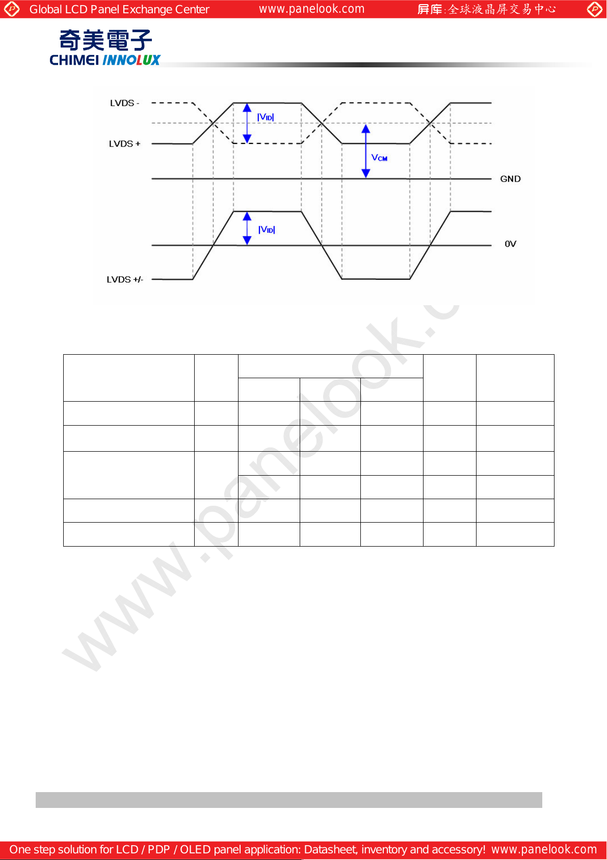
3. ELECTRICAL CHARACTERISTICS
3.1 TFT LCD MODULE
(Ta = 25 ± 2 ºC)
Parameter Symbol
Power Supply Voltage VCC 4.5 5.0 5.5 V -
PRODUCT SPECIFICATION
Value
Unit Note
Min. Typ. Max.
Rush Current I
RUSH
Power consumption P
White Pattern
Power Supply Current
Vertical Stripe
Black Pattern
LVDS
interface
Differential Input High
Threshold Voltage
Differential Input Low
Threshold Voltage
Common Input Voltage VCM 1.0 1.2 1.4 V
Differential input voltage |VID| 200
V
V
Terminating Resistor RT
T
LVTH
LVTL
+100
Note (1) The module should be always operated within above ranges.
Note (2) Power on rush current measurement conditions:
3 A
3.0 4.5 Watt (4)
0.44 0.6 A (3)a
0.6 0.9 A (3)c
0.58 0.9 A (3)b
mV
-100 mV
100
600 mV (5)
ohm
+5.0V
R1
47K
Q1
2SK1475
FUSE
C3
1uF
(LCD Module Input)
(Control Signal)
SW
+12V
C1
1uF
VR1
47K
R2
1K
0.01uF
Q2
2SK1470
C2
Version 2.2 8 D a t e
28 O c t 20 10
The copyright belongs to CHIMEI Innolux. Any unauthorized use is prohibited
Vcc
Page 9
Global LCD Panel Exchange Center
www.panelook.com
One step solution for LCD / PDP / OLED panel application: Datasheet, inventory and accessory!
www.panelook.com
R
Vcc rising time is 470µs
0.1Vcc
GND
Note (3) The specified power supply current is under the conditions at Vcc = 5.0 V, Ta = 25 ± 2 ºC, fv = 60
PRODUCT SPECIFICATION
Vcc
470µs
Hz, whereas a power dissipation check pattern below is displayed.
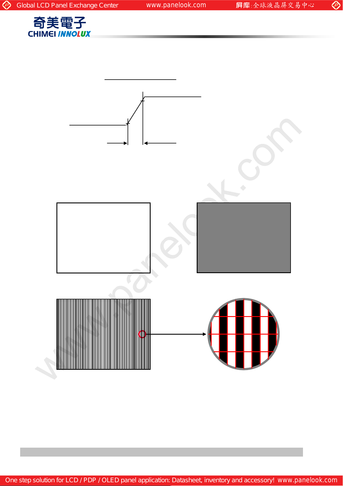
a. White Pattern
Active Area
c. Vertical Stripe Pattern
b. Black Pattern
Active Area
R
G
R
B
G
R
B
G
R
G
R
G
B
B
B
B
B
R
G
B
R
R
G
B
R
G
B
Note (4) The power consumption is specified at the pattern with the maximum current.
Note (5) VID waveform condition
Active Area
Version 2.2 9 D a t e
The copyright belongs to CHIMEI Innolux. Any unauthorized use is prohibited
28 O c t 20 10
Page 10
Global LCD Panel Exchange Center
www.panelook.com
One step solution for LCD / PDP / OLED panel application: Datasheet, inventory and accessory!
www.panelook.com
PRODUCT SPECIFICATION
3.2 BACKLIGHT CONNECTOR PIN CONFIGURATION
3.2.1 LAMP SPECIFICATION
Parameter Symbol
Min. Typ. Max.
Lamp Input Voltage VW - 760 836- V
Lamp Current IL 2.0 7.0 8.0 mA
- -
Lamp Turn On Voltage VS
- -
Operating Frequency FO 40 - 80 KHz (3)
Lamp Life Time LBL 50,000 - - Hrs (5), IL = 7.0mA
Value
1460(25)
1680(0)
(Ta = 25 ± 2 ºC)
Unit Note
IL=7.0mA
RMS
(1)
RMS
VRMS (2)
VRMS (2)
Version 2.2 10 D a t e
The copyright belongs to CHIMEI Innolux. Any unauthorized use is prohibited
28 O c t 20 10
Page 11

Global LCD Panel Exchange Center
www.panelook.com
One step solution for LCD / PDP / OLED panel application: Datasheet, inventory and accessory!
www.panelook.com
Oscilloscope
PRODUCT SPECIFICATION
Note (1) Lamp current is measured by current amplify & oscilloscope as shown below:
Measure equipment:
Current Amplify: Tektronix TCPA300
Current probe: Tektronix TCP312
Oscilloscope: TDS3054B
LCD
Module
Note (2) The voltage that must be larger than Vs should be applied to the lamp for more than 1 second after
startup. Otherwise, the lamp may not be turned on normally. It is the value output voltage of NF
circuit.
Note (3) The lamp frequency may produce interference with horizontal synchronization frequency from the
display, which might cause line flow on the display. In order to avoid interference, the lamp
frequency should be detached from the horizontal synchronization frequency and its harmonics as
HV (Pink)
LV (White)
HV (Pink)
LV (White)
Current
Probe
1
2
1
2
A
A
Inverter
Current
Amplify
far as possible.
Note (4) PL = IL V
Note (5) The lifetime of lamp can be defined as the time in which it continues to operate under the condition
Ta = 25 2 oC and( IL = 7.0 mArms )until one of the following events occurs:
(a) When the brightness becomes 50% of its original value.
(b) When the effective ignition length becomes 80% of its original value.
(The effective ignition length is a scope that luminance is over 80% of that at the center point.)
Note (6) The waveform of the voltage output of inverter must be area-symmetric and the design of the
inverter must have specifications for the modularized lamp. The performance of the Backlight, such
as lifetime or brightness, is greatly influenced by the characteristics of the DC-AC inverter for the
lamp. All the parameters of an inverter should be carefully designed to avoid producing too much
current leakage from high voltage output of the inverter. When designing or ordering the inverter
please make sure that a poor lighting caused by the mismatch of the Backlight and the inverter
(miss-lighting, flicker, etc.) never occurs. If the above situation is confirmed, the module should be
operated in the same manners when it is installed in your instrument.
The output of the inverter must have symmetrical (negative and positive) voltage waveform and
2 (for 2 lamps)
L
symmetrical current waveform.(Unsymmetrical ratio is less than 10%) Please do not use the inverter
which has unsymmetrical voltage and unsymmetrical current and spike wave. Lamp frequency may
produce interface with horizontal synchronous frequency and as a result this may cause beat on the
display. Therefore lamp frequency shall be as away possible from the horizontal synchronous frequency
Version 2.2 11 D a t e
The copyright belongs to CHIMEI Innolux. Any unauthorized use is prohibited
28 O c t 20 10
Page 12

Global LCD Panel Exchange Center
www.panelook.com
One step solution for LCD / PDP / OLED panel application: Datasheet, inventory and accessory!
www.panelook.com
SCAN DRIVER IC
Vcc
PRODUCT SPECIFICATION
and from its harmonics in order to prevent interference.
Requirements for a system inverter design, which is intended to have a better display performance, a
better power efficiency and a more reliable lamp. It shall help increase the lamp lifetime and reduce its
leakage current.
a. The asymmetry rate of the inverter waveform should be 10% below;
b. The distortion rate of the waveform should be within 2 ± 10%;
c. The ideal sine wave form shall be symmetric in positive and negative polarities
* Asymmetry rate:
I p
| I p – I –p | / I
* 100%
rms
I -p
4. BLOCK DIAGRAM OF INTERFACE
4.1 TFT LCD MODULE
RX0(+/-)
RX1(+/-)
RX2(+/-)
RX3(+/-)
RXC(+/-)
NC
GND
INPUT CONNECTOR
TIMING CONTROLLER
DC/DC CONVERTER &
REFERENCE VOLTAGE
* Distortion rate
I p (or I –p) / I
LVDS INPUT /
rms
TFT LCD PANEL
(1366x3x768)
DATA
VL
LAMP CONNECTOR
(YEONHO 35001HS-02L)
BACKLIGHT
Version 2.2 12 D a t e
28 O c t 20 10
The copyright belongs to CHIMEI Innolux. Any unauthorized use is prohibited
Page 13

Global LCD Panel Exchange Center
www.panelook.com
One step solution for LCD / PDP / OLED panel application: Datasheet, inventory and accessory!
www.panelook.com
1 (JAE)
5. INPUT TERMINAL PIN ASSIGNMENT
5.1 TFT LCD Module Input
Pin Name Description
1 NC Not connection, this pin should be open.
2 NC Not connection, this pin should be open.
3 NC Not connection, this pin should be open.
4 GND Ground
5 RX0- Negative LVDS differential data input. Channel 0
6 RX0+ Positive LVDS differential data input. Channel 0
7 GND Ground
8 RX1- Negative LVDS differential data input. Channel 1
9 RX1+ Positive LVDS differential data input. Channel 1
10 GND Ground
11 RX2- Negative LVDS differential data input. Channel 2
12 RX2+ Positive LVDS differential data input. Channel 2
13 GND Ground
14 RXCLK- Negative LVDS differential clock input.
15 RXCLK+ Positive LVDS differential clock input.
16 GND Ground
17 RX3- Negative LVDS differential data input. Channel 3
18 RX3+ Positive LVDS differential data input. Channel 3
19 GND Ground
20 NC Not connection, this pin should be open.
21 NC Not connection, this pin should be open.
22 NC Not connection, this pin should be open.
23 GND Ground
24 GND Ground
25 GND Ground
26 Vcc +5.0V power supply
27 Vcc +5.0V power supply
28 Vcc +5.0V power supply
29 Vcc +5.0V power supply
30 Vcc +5.0V power supply
PRODUCT SPECIFICATION
Note (1) Connector Part No.: 093G30-B0001A(STARCONN) or MSAKT2407P30HA (STM )
Note (2) Mating Wire Cable Connector Part No.: FI-X30H(JAE) or FI-X30HL(JAE)
Note (3) Mating FFC Cable Connector Part No.: 217007-013001 (P-TWO) or JF05X030Note (4) The first pixel is odd.
Note (5) Input signal of even and odd clock should be the same timing.
Version 2.2 13 D a t e
The copyright belongs to CHIMEI Innolux. Any unauthorized use is prohibited
28 O c t 20 10
Page 14

Global LCD Panel Exchange Center
www.panelook.com
One step solution for LCD / PDP / OLED panel application: Datasheet, inventory and accessory!
www.panelook.com
5.2 BACKLIGHT UNIT
The pin configuration for the housing and the leader wire is shown in the table below.
Pin Name Description Wire Color
1 HV High Voltage Pink
2 LV Low Voltage White
Note (1) Connector Part No.: YEONHO 35001HS-02L or equivalent
PRODUCT SPECIFICATION
1 HV(Pink)
2 LV(White)
1 HV(Pink)
2 LV(White)
Version 2.2 14 D a t e
The copyright belongs to CHIMEI Innolux. Any unauthorized use is prohibited
28 O c t 20 10
Page 15

Global LCD Panel Exchange Center
www.panelook.com
One step solution for LCD / PDP / OLED panel application: Datasheet, inventory and accessory!
www.panelook.com
5.3 BLOCK DIAGRAM OF INTERFACE
50
50
50
50
50
50
50
PRODUCT SPECIFICATION
50
50
50
AR0~AR7 Even pixel R data
AG0~AG7 Even pixel G data
AB0~AB7 Even pixel B data
DE Data enable signal
DCLK Data clock signal
Note (1) The system must have the transmitter to drive the module.
Note (2) LVDS cable impedance shall be 50 ohms per signal line or about 100 ohms per twist-pair line when it is
used differentially.
Note (3) Two pixel data send into the module for every clock cycle. The first pixel of the frame is odd pixel and the
second pixel is even pixel.
Version 2.2 15 D a t e
The copyright belongs to CHIMEI Innolux. Any unauthorized use is prohibited
28 O c t 20 10
Page 16

Global LCD Panel Exchange Center
www.panelook.com
One step solution for LCD / PDP / OLED panel application: Datasheet, inventory and accessory!
www.panelook.com
5.4 LVDS INTERFACE
VESA Format :
PRODUCT SPECIFICATION
AR0~AR7 : First Pixel R Data (7; MSB, 0; LSB)
AG0~AG7 : First Pixel G Data (7; MSB, 0; LSB)
AB0~AB7 : First Pixel B Data (7; MSB, 0; LSB)
DE : Data enable signal
DCLK : Data clock signal
Version 2.2 16 D a t e
The copyright belongs to CHIMEI Innolux. Any unauthorized use is prohibited
28 O c t 20 10
Page 17

Global LCD Panel Exchange Center
www.panelook.com
One step solution for LCD / PDP / OLED panel application: Datasheet, inventory and accessory!
www.panelook.com
5.5 COLOR DATA INPUT ASSIGNMENT
The brightness of each primary color (red, green and blue) is based on the 8-bit gray scale data input for
the color. The higher the binary input, the brighter the color. The table below provides the assignment of
color versus data input.
Color
R7 R6 R5 R4 R3 R2 R1 R0 G7 G6 G5 G4 G3 G2 G1 G0 B7 B6 B5 B4 B3 B2 B1 B0
Basic
Colors
Gray
Scale
Of
Red
Black
Green
Cyan
Magenta
Yellow
White
Red(0) / Dark
Red(1)
Red(2)
Red(253)
Red(254)
Red(255)
Red
Blue
0
0
0
1
1
1
0
0
0
0
0
0
0
0
0
1
1
1
1
1
1
1
1
1
0
0
0
0
0
0
0
0
0
:
:
:
:
:
:
1
1
1
1
1
1
1
1
1
PRODUCT SPECIFICATION
Data Signal
Red Green Blue
0
0
0
0
0
0
0
0
0
0
0
0
0
0
0
1
1
1
1
1
0
0
0
0
0
0
0
0
0
0
0
0
0
0
0
1
1
1
1
1
1
1
1
0
0
0
0
0
0
0
0
0
0
0
0
0
0
0
1
1
0
0
0
0
0
1
1
1
1
1
1
1
1
1
1
1
1
1
1
1
0
0
0
0
0
0
0
0
1
1
1
1
1
1
1
1
1
1
1
1
1
1
1
0
0
1
1
1
1
1
1
1
1
1
1
1
1
1
1
1
0
0
0
0
0
0
0
0
0
0
0
0
0
0
0
0
0
0
0
1
0
0
0
0
0
0
0
0
0
0
0
0
0
1
0
0
0
0
0
0
0
0
0
0
0
:
:
:
:
:
:
:
:
:
:
:
:
:
:
:
:
:
:
:
:
:
:
:
:
:
:
:
:
:
:
:
:
1
1
1
0
1
0
0
0
0
0
0
0
0
0
0
1
1
1
1
0
0
0
0
0
0
0
0
0
0
0
1
1
1
1
1
0
0
0
0
0
0
0
0
0
0
0
0
0
0
0
0
0
0
0
0
0
0
0
0
0
0
0
0
1
1
1
1
1
1
1
1
1
1
1
1
1
1
1
1
1
1
0
0
0
0
0
0
1
1
1
1
1
1
0
0
0
0
0
0
0
0
0
0
0
0
0
0
0
0
0
0
:
:
:
:
:
:
:
:
:
:
:
:
0
0
0
0
0
0
0
0
0
0
0
0
0
0
0
0
0
0
Green(0) / Dark
Gray
Scale
Of
Green
Gray
Scale
Of
Blue
Note (1) 0: Low Level Voltage, 1: High Level Voltage
Green(1)
Green(2)
Green(253)
Green(254)
Green(255)
Blue(0) / Dark
Blue(1)
Blue(2)
Blue(253)
Blue(254)
Blue(255)
0
0
0
0
0
0
0
0
0
0
0
0
0
0
0
0
0
0
0
0
0
:
:
:
:
:
:
:
:
:
:
:
:
:
:
:
:
0
0
0
0
0
0
0
0
0
0
0
0
0
0
0
0
0
0
0
0
0
0
0
0
0
0
0
0
0
0
0
0
0
0
0
0
0
0
0
0
0
0
:
:
:
:
:
:
:
:
:
:
:
:
:
:
:
:
0
0
0
0
0
0
0
0
0
0
0
0
0
0
0
0
0
0
0
0
0
0
0
0
0
0
0
0
0
0
0
0
0
0
0
0
0
0
0
0
0
0
0
0
0
0
1
0
0
0
0
0
0
0
0
0
0
0
0
0
0
0
1
0
0
0
0
0
0
0
0
0
:
:
:
:
:
:
:
:
:
:
:
:
:
:
:
:
:
:
:
:
:
:
:
:
:
:
:
:
:
:
:
:
:
:
0
1
1
1
1
1
1
0
1
0
0
0
0
0
0
0
0
0
1
1
1
1
1
1
1
0
0
0
0
0
0
0
0
0
0
1
1
1
1
1
1
1
1
0
0
0
0
0
0
0
0
0
0
0
0
0
0
0
0
0
0
0
0
0
0
0
0
0
0
0
0
0
0
0
0
0
0
0
0
0
0
0
0
0
1
0
0
0
0
0
0
0
0
0
0
0
0
0
0
0
1
0
:
:
:
:
:
:
:
:
:
:
:
:
:
:
:
:
:
:
:
:
:
:
:
:
:
:
:
:
:
:
:
:
:
:
0
0
0
0
0
0
0
0
0
1
1
1
1
1
1
0
1
0
0
0
0
0
0
0
0
0
1
1
1
1
1
1
1
0
0
0
0
0
0
0
0
0
0
1
1
1
1
1
1
1
1
Version 2.2 17 D a t e
The copyright belongs to CHIMEI Innolux. Any unauthorized use is prohibited
28 O c t 20 10
Page 18

Global LCD Panel Exchange Center
www.panelook.com
One step solution for LCD / PDP / OLED panel application: Datasheet, inventory and accessory!
www.panelook.com
6. INTERFACE TIMING
6.1 INPUT SIGNAL TIMING SPECIFICATIONS
(Ta = 25 ± 2 ºC)
The input signal timing specifications are shown as the following table and timing diagram.
PRODUCT SPECIFICATION
Signal Item Symbol
F
(=1/TC)
clkin_mod
F
F
LVDS
Receiver
Clock
LVDS
Receiver
Data
Vertical
Active
Display
Term
Horizontal
Active
Display
Term
Frequency
Input cycle to
cycle jitter
Spread spectrum
modulation range
Spread spectrum
modulation frequency
Setup Time Tlvsu
Hold Time Tlvhd
Frame Rate Fr5 50 60 75 Hz Tv=Tvd+Tvb
Total Tv 800 806 815 Th
Display Tvd 768 768 768 Th
Blank Tvb Tv-Tvd 38 Tv-Tvd Th
Total Th 1500 1560 1570 Tc Th=Thd+Thb
Display Thd 1366 1366 1366 Tc
Blank Thb Th-Thd 194 Th-Thd Tc
clkin
T
SSM
rcl
Min. Typ. Max. Unit Note
60 76 96 MHz
Fc*98%
600
600
200 ps (1)
Fc* 102%
200 KHz
MHz
ps
ps
(2)
(3)
Note: Because this module is operated by DE only mode, Hsync and Vsync input signals are ignored.
INPUT SIGNAL TIMING DIAGRAM
DE
Th
DCLK
DE
DATA
TC
Thb
Thd
Version 2.2 18 D a t e
The copyright belongs to CHIMEI Innolux. Any unauthorized use is prohibited
28 O c t 20 10
Page 19

Global LCD Panel Exchange Center
www.panelook.com
One step solution for LCD / PDP / OLED panel application: Datasheet, inventory and accessory!
www.panelook.com
14
14
14
14
14
14
14
PRODUCT SPECIFICATION
Note (1) The input clock cycle-to-cycle jitter is defined as below figures. Trcl = I T1 – TI
T1
Note (2) The SSCG (Spread spectrum clock generator) is defined as below figures.
Note (3) The LVDS timing diagram and setup/hold time is defined and showing as the following figures.
RXCLK+/-
RXn+/-
Tlvs
Tlvh
1cT
LVDS RECEIVER INTERFACE TIMING DIAGRAM
Tc
3cT
5cT
7cT
9cT
11cT
13cT
Version 2.2 19 D a t e
The copyright belongs to CHIMEI Innolux. Any unauthorized use is prohibited
28 O c t 20 10
Page 20

Global LCD Panel Exchange Center
www.panelook.com
One step solution for LCD / PDP / OLED panel application: Datasheet, inventory and accessory!
www.panelook.com
-
PRODUCT SPECIFICATION
6.2 POWER ON/OFF SEQUENCE
To prevent a latch-up or DC operation of LCD module, the power on/off sequence should be as the
diagram below.
Power Supply
for LCD, Vcc
Interface Signal
(LVDS Signal of
Transmitter), VI
-
Power for Lamp
Timing Specifications:
0.5< t1 5 msec
0 < t2 50 msec
0 < t3 50 msec
0V
0V
Power On
90%
10%
t1
OFF
t2
50%
Valid Data
ON
Power Off
90%
t3
t6 t5
50%
OFF
t7
10%
Restart
10%
t4
t4 500 msec
t5 450 msec
t6 90 msec
5 t7 100 msec
Note.
(1) The supply voltage of the external system for the module input should be the same as the definition of Vcc.
(2) Apply the lamp voltage within the LCD operation range. When the backlight turns on before the LCD
operation of the LCD turns off, the display may momentarily become abnormal screen.
(3) In case of VCC = off level, please keep the level of input signals on the low or keep a high impedance.
(4) T4 should be measured after the module has been fully discharged between power off and on period.
(5) Interface signal shall not be kept at high impedance when the power is on.
(6) CMO won’t take any responsibility for the products which are damaged by the customers not following the
Power Sequence.
(7) There might be slight electronic noise when LCD is turned off (even backlight unit is also off). To avoid this
symptom, we suggest "Vcc falling timing" to follow "t7 spec".
Version 2.2 20 D a t e
28 O c t 20 10
The copyright belongs to CHIMEI Innolux. Any unauthorized use is prohibited
Page 21

Global LCD Panel Exchange Center
www.panelook.com
One step solution for LCD / PDP / OLED panel application: Datasheet, inventory and accessory!
www.panelook.com
7. OPTICAL CHARACTERISTICS
7.1 TEST CONDITIONS
Item Symbol Value Unit
PRODUCT SPECIFICATION
Ambient Temperature Ta
Ambient Humidity Ha
Supply Voltage VCC 5 V
Input Signal According to typical value in "3. ELECTRICAL CHARACTERISTICS"
Lamp Current IL 7.0±0.5 mA
Oscillating Frequency (Inverter)
Vertical Frame Rate Fr 60 Hz
FW 55±5 KHz
25±2
50±10
o
C
%RH
Version 2.2 21 D a t e
The copyright belongs to CHIMEI Innolux. Any unauthorized use is prohibited
28 O c t 20 10
Page 22

Global LCD Panel Exchange Center
www.panelook.com
One step solution for LCD / PDP / OLED panel application: Datasheet, inventory and accessory!
www.panelook.com
7.2 OPTICAL SPECIFICATIONS
The relative measurement methods of optical characteristics are shown in 7.2. The following items should be
measured under the test conditions described in 7.1 and stable environment shown in 7.1.
PRODUCT SPECIFICATION
Item Symbol
Contrast Ratio CR
TR -
Response Time (TN)
TF
Center Luminance of White LC
White Variation
δ
W
Condition Min. Typ. Max. Unit Note
θ
=0°,
θ
θ
θ
θ
=0°
Y
=0°
Y
=0°
Y
=0°
Y
700 1000 - - (2).(5)
1.3 2.2-
-
3.7 5.8
250 300 - cd/m
ms
ms
2
(4).(5)
- 1.3 1.5 - (5).(6)
x
CS-1000T
θ
=0°,
x
θ
=0°,
x
CS-1000T
θ
=0°,
x
USB2000
(3)
Cross Talk CT - - 4 % (7)
Rx 0.646 -
Red
Ry 0.334 -
Gx 0.284 -
Green
Color
Chromaticity
Blue
Gy 0.602 -
Bx 0.152 -
θ
=0°,
θ
x
CS-1000T
=0°
Y
Typ
-0.03
Typ.
+0.03
(1).(5)
By 0.076 -
Viewing
Angle
Wx 0.313 -
White
Wy
Color Gamut C.G -
Horizontal
θ
x+ + θx-
150 170
CR≥10 (TN)
Vertical
θ
Y+ + θY-
140 160
0.329
-
72 - % NTSC
-
Deg. (1).(5)
-
-
Version 2.2 22 D a t e
28 O c t 20 10
The copyright belongs to CHIMEI Innolux. Any unauthorized use is prohibited
Page 23

Global LCD Panel Exchange Center
www.panelook.com
One step solution for LCD / PDP / OLED panel application: Datasheet, inventory and accessory!
www.panelook.com
θ
y+
= 90º
θ
y
-
= 90º
θx−
θx+
θ
x = θy = 0º
Gray
L
evel 0
Gray
L
evel
255
Note (1) Definition of Viewing Angle (θx, θy):
PRODUCT SPECIFICATION
Normal
θy- θy+
θX-
= 90º
6 o’clock
x-
y-
Note (2) Definition of Contrast Ratio (CR):
The contrast ratio can be calculated by the following expression.
Contrast Ratio (CR) = L255 / L0
L255: Luminance of gray level 255
L 0: Luminance of gray level 0
CR = CR (5)
CR (X) is corresponding to the Contrast Ratio of the point X at Figure in Note (6).
12 o’clock direction
y+
x+
θX+
= 90º
Note (3) Definition of Response Time (TR, TF):
100%
90%
Optical
Response
Gray Level 255
10%
0%
T
T
R
F
66.67ms 66.67ms
Version 2.2 23 D a t e
28 O c t 20 10
The copyright belongs to CHIMEI Innolux. Any unauthorized use is prohibited
Page 24

Global LCD Panel Exchange Center
www.panelook.com
One step solution for LCD / PDP / OLED panel application: Datasheet, inventory and accessory!
www.panelook.com
LCD
P
anel
Center of the
S
creen
CS2000
Note (4) Definition of Luminance of White (LC):
PRODUCT SPECIFICATION
Measure the luminance of gray level 255 at center point
LC = L (5)
L (x) is corresponding to the luminance of the point X at Figure in Note (6).
Note (5) Measurement Setup:
The LCD module should be stabilized at given temperature for 30 minutes to avoid abrupt
temperature change during measuring. In order to stabilize the luminance, the measurement
should be executed after lighting Backlight for 30 minutes in a windless room.
LCD Module
USB2000
CS-1000T
Note (6) Definition of White Variation (δW):
Measure the luminance of gray level 255 at 9 points
δ
W = Maximum [L (1), L (2) ……L (4), L (9)] / Minimum [L (1), L (2) …… L (4), L (9)]
W/10
Vertical Line
W
W/2
9W/10
Light Shield Room
(Ambient Luminance < 2 lux)
Horizontal Line
D
D/10
1
4
7 8 9
D/2
2
5
9D/10
3
6
: Test Point
X
X=1 to 9
Version 2.2 24 D a t e
The copyright belongs to CHIMEI Innolux. Any unauthorized use is prohibited
Active Area
28 O c t 20 10
Page 25

Global LCD Panel Exchange Center
www.panelook.com
One step solution for LCD / PDP / OLED panel application: Datasheet, inventory and accessory!
www.panelook.com
Active Area
Active Area
(D, W)
Note (7) Definition of Cross Talk (CT):
CT = | YB – YA | / YA × 100 (%)
Where:
YA = Luminance of measured location without gray level 0 pattern (cd/m2)
YB = Luminance of measured location with gray level 0 pattern (cd/m2)
PRODUCT SPECIFICATION
(0, 0)
(0, 0)
Y
(D/2,W/8)
A, U
(D/4,W/4)
Y
B, U
(D/2,W/8)
Y
(D/8,W/2)
A, L
Gray 128
Y
(7D/8,W/2)
A, R
Y
(D/8,W/2)
B, L
BACKLIGH
Y
(7D/8,W/2)
B, R
Y
(D/2,7W/8)
A, D
(D, W)
(3D/4,3W/4)
Y
(D/2,7W/8)
B, D
Version 2.2 25 D a t e
28 O c t 20 10
The copyright belongs to CHIMEI Innolux. Any unauthorized use is prohibited
Page 26

Global LCD Panel Exchange Center
www.panelook.com
One step solution for LCD / PDP / OLED panel application: Datasheet, inventory and accessory!
www.panelook.com
PRODUCT SPECIFICATION
8. PRECAUTIONS
8.1 ASSEMBLY AND HANDLING PRECAUTIONS
(1) Do not apply rough force such as bending or twisting to the module during assembly.
(2) To assemble or install module into user’s system can be only in clean working areas. The dust and oil
may cause electrical short or worsen the polarizer.
(3) It’s not permitted to have pressure or impulse on the module because the LCD panel and Backlight will
be damaged.
(4) Always follow the correct power sequence when LCD module is connecting and operating. This can
prevent damage to the CMOS LSI chips during latch-up.
(5) Do not pull the I/F connector in or out while the module is operating.
(6) Do not disassemble the module.
(7) Use a soft dry cloth without chemicals for cleaning, because the surface of polarizer is very soft and
easily scratched.
(8) It is dangerous that moisture come into or contacted the LCD module, because moisture may damage
LCD module when it is operating.
(9) High temperature or humidity may reduce the performance of module. Please store LCD module within
the specified storage conditions.
(10) When ambient temperature is lower than 10ºC may reduce the display quality. For example, the
response time will become slowly, and the starting voltage of CCFL will be higher than room
temperature.
8.2 SAFETY PRECAUTIONS
(1) The startup voltage of Backlight is approximately 1000 Volts. It may cause electrical shock while
assembling with inverter. Do not disassemble the module or insert anything into the Backlight unit.
(2) If the liquid crystal material leaks from the panel, it should be kept away from the eyes or mouth. In
case of contact with hands, skin or clothes, it has to be washed away thoroughly with soap.
(3) After the module’s end of life, it is not harmful in case of normal operation and storage.
Version 2.2 26 D a t e
The copyright belongs to CHIMEI Innolux. Any unauthorized use is prohibited
28 O c t 20 10
Page 27

Global LCD Panel Exchange Center
www.panelook.com
One step solution for LCD / PDP / OLED panel application: Datasheet, inventory and accessory!
www.panelook.com
PRODUCT SPECIFICATION
9. DEFINITION OF LABELS
9.1 CMI MODULE LABEL
The barcode nameplate is pasted on each module as illustration, and its definitions are as following explanation.
(a) Model Name: V185B1-L03
(b) Revision: Rev. XX, for example: A0, A1… B1, B2… or C1, C2…etc.
(c) CMO barcode definition:
Serial ID: XX-XX-X-XX-YMD-L-NNNN
Code
XX CMO internal use XX Revision Cover all the change
X CMO internal use -
XX CMO internal use -
YMD Year, month, day
L Product line # Line 1=1, Line 2=2, Line 3=3, …
NNNN Serial number Manufacturing sequence of product
(d) Customer’s barcode definition:
Serial ID: CM-18B13-X-X-X-XX-L-XX-L-YMD-NNNN
Code
CM Supplier code CMO=CM
18B13 Model number V185B1-L03 = 18B13
X Revision code Non ZBD: 1,2,~,8,9 / ZBD: A~Z
X Source driver IC code
X Gate driver IC code
Meaning Description
Year:0~9, 2001=1, 2002=2, 2003=3…2010=0,2011=1,2012=2…
Month: 1~12=1, 2, 3, ~, 9, A, B, C
Day: 1~31=1, 2, 3, ~, 9, A, B, C, ~, W, X, Y, exclude I, O, and U.
Meaning Description
Century=1, CLL=2, Demos=3, Epson=4, Fujitsu=5, Himax=6,
Hitachi=7, Hynix=8, LDI=9, Matsushita=A, NEC=B, Novatec=C,
OKI=D, Philips=E, Renasas=F, Samsung=G, Sanyo=H, Sharp=I,
TI=J, Topro=K, Toshiba=L,Windbond=M
XX Cell location Tainan Taiwan=TN, Ningbo China=NP
L Cell line # 1,2,~,9,A,B,~,Y,Z
XX Module location Tainan Taiwan=TN, Ningbo China=NP
L Module line # 1,2,~,9,A,B,~,Y,Z
Year:0~9,2001=1,2002=2, 2003=3…2010=0, 2011=1, 2012=2…
YMD Year, month, day
NNNN Serial number By LCD supplier
Version 2.2 27 D a t e
The copyright belongs to CHIMEI Innolux. Any unauthorized use is prohibited
Month: 1~12=1, 2, 3, ~, 9, A, B, C
Day: 1~31=1, 2, 3, ~, 9, A, B, C, ~, T, U, V
28 O c t 20 10
Page 28

Global LCD Panel Exchange Center
www.panelook.com
One step solution for LCD / PDP / OLED panel application: Datasheet, inventory and accessory!
www.panelook.com
(e) FAB ID(UL Factory ID):
Region Factory ID
TWCMO
NBCMO LEOO
NBCME CANO
NHCMO CAPG
GEMN
10. PACKAGING
10.1 PACKAGING SPECIFICATIONS
(1) 9 LCD modules / 1 Box
(2) Box dimensions: 525(L) X 284 (W) X 360 (H) mm
(3) Weight: 19.40 Kg (9 modules per box)
PRODUCT SPECIFICATION
10.2 PACKAGING METHOD
(1) Carton Packing should have no failure in the following reliability test items.
Test Item Test Conditions Note
ISTA STANDARD
Random, Frequency Range: 1 – 200 Hz
Vibration
Dropping Test 1 Corner, 3 Edge, 6 Face, ISTA STANDARD Non Operation
Top & Bottom: 30 minutes (+Z), 10 min (-Z),
Right & Left: 10 minutes (X)
Back & Forth 10 minutes (Y)
Non Operation
Figure.10-1 Packing method
Version 2.2 28 D a t e
The copyright belongs to CHIMEI Innolux. Any unauthorized use is prohibited
28 O c t 20 10
Page 29

Global LCD Panel Exchange Center
www.panelook.com
One step solution for LCD / PDP / OLED panel application: Datasheet, inventory and accessory!
www.panelook.com
PRODUCT SPECIFICATION
Sea / Land Transportation (40ft HQ Container)
PP Belt
Corner
Protector
(50*50*1000mm)
PE
Sheet
Film
Corner
Protector
(50*50*1000mm)
PE
Sheet
Film
Carton
Label
Corner
Protector
(50*50*1000mm)
Pallet
(1150*1080*143mm)
Sea / Land Transportation (40ft Container)
PP Belt
Corner
Protector
(50*50*1000mm)
PE
Sheet
Film
PE
Sheet
Film
Carton
Label
Corner
Protector
(50*50*625mm)
Corner
Protector
(50*50*1000mm)
Pallet
(1150*1080*143mm)
Air Transportation
PP Belt
Corner
Protector
(50*50*1000mm)
PE
Sheet
Film
Carton
Label
Pallet
(1150*1080*143mm)
Corner
Protector
(50*50*1000mm)
Figure. 10-2 Packing method
Version 2.2 29 D a t e
28 O c t 20 10
The copyright belongs to CHIMEI Innolux. Any unauthorized use is prohibited
Page 30

Global LCD Panel Exchange Center
www.panelook.com
One step solution for LCD / PDP / OLED panel application: Datasheet, inventory and accessory!
www.panelook.com
11. MECHANICAL CHARACTERISTIC
[Refer to the next 2 pages]
PRODUCT SPECIFICATION
Version 2.2 30 D a t e
The copyright belongs to CHIMEI Innolux. Any unauthorized use is prohibited
28 O c t 20 10
Page 31

Global LCD Panel Exchange Center
www.panelook.com
One step solution for LCD / PDP / OLED panel application: Datasheet, inventory and accessory!
www.panelook.com
PRODUCT SPECIFICATION
Version 2.2 31 D a t e
The copyright belongs to CHIMEI Innolux. Any unauthorized use is prohibited
28 O c t 20 10
 Loading...