

Page 1
Global LCD Panel Exchange Center
Issued Date: Mar. 12, 2008
www.panelook.com
DOC No.:
Model No.: S220Z1-M02
Ten tative
Specifications
Model No : S220Z1 – M02
Customer :
Approved by :
Note :
Liquid Crystal Display Division
QRA Division. OA Head Division.
Approval Approval
1 / 29
One step solution for LCD / PDP / OLED panel application: Datasheet, inventory and accessory!
Version 0.0
www.panelook.com
Page 2
Global LCD Panel Exchange Center
Issued Date: Mar. 12, 2008
www.panelook.com
DOC No.:
Model No.: S220Z1-M02
Ten tative
- CONTENTS -
REVISION HISTORY
-------------------------------------------------------
3
1. GENERAL DESCRIPTION
1.1 OVERVIEW
1.2 FEATURES
1.3 APPLICATION
1.4 GENERAL SPECIFICATIONS
1.5 MECHANICAL SPECIFICATIONS
2. ABSOLUTE MAXIMUM RATINGS
2.1 ABSOLUTE RATINGS OF ENVIRONMENT
2.2 ELECTRICAL ABSOLUTE RATINGS
2.2.1 TFT LCD MODULE
2.2.2 BACKLIGHT UNIT
3. ELECTRICAL CHARACTERISTICS
3.1 TFT LCD MODULE
3.2 BACKLIGHT UNIT
4. BLOCK DIAGRAM
4.1 TFT LCD MODULE
4.2 BACKLIGHT UNIT
5. INPUT TERMINAL PIN ASSIGNMENT
5.1 TFT LCD MODULE
5.2 BACKLIGHT UNIT
5.3 COLOR DATA INPUT ASSIGNMENT
-------------------------------------------------------
-------------------------------------------------------
-------------------------------------------------------
-------------------------------------------------------
-------------------------------------------------------
4
5
7
11
12
6. INTERFACE TIMING
6.1 INPUT SIGNAL TIMING SPECIFICATIONS
6.2 POWER ON/OFF SEQUENCE
-------------------------------------------------------
15
7. DRIVER DC CHARACTERISTIC ------------------------------------------------- 17
7.1 RSDS CHARACTERISTICS
7.2 Electrical Characteristics
8. Driver AC CHARACTERISTICS ------------------------------------------------- 19
9. VERTICAL TIMING ------------------------------------------------- 20
10. OPTICAL CHARACTERISTICS
10.1 TEST CONDITIONS
10.2 OPTICAL SPECIFICATIONS
11. PACKAGING
11.1 PACKING SPECIFICATIONS
11.2 PACKING METHOD
12. DEFINITION OF LABELS
13. PRECAUTIONS
10.1 ASSEMBLY AND HANDLING PRECAUTIONS
10.2 SAFETY PRECAUTIONS
-------------------------------------------------------
-------------------------------------------------------
-------------------------------------------------------
-------------------------------------------------------
21
24
25
26
14. MECHANICAL CHARACTERISTICS
-------------------------------------------------------
2 / 29
One step solution for LCD / PDP / OLED panel application: Datasheet, inventory and accessory!
27
Version 0.0
www.panelook.com
Page 3
Global LCD Panel Exchange Center
Issued Date: Mar. 12, 2008
www.panelook.com
DOC No.:
Model No.: S220Z1-M02
Ten tative
REVISION HISTORY
Date Section Description
0.0 Mar, 12, 08’ - S220Z1 Tentative Specifications was first issued.
3 / 29
One step solution for LCD / PDP / OLED panel application: Datasheet, inventory and accessory!
Version 0.0
www.panelook.com
Page 4
Global LCD Panel Exchange Center
Issued Date: Mar. 12, 2008
www.panelook.com
DOC No.:
Model No.: S220Z1-M02
Ten tative
1. GENERAL DESCRIPTION
1.1 OVERVIEW
S220Z1-M02 is a 22” wide TFT Liquid Crystal Display module with 4 CCFL Backlight unit and a 30-pin
TMDS interface. This module supports 1680 x 1050 WSXGA+ (16:10 wide screen) mode and displays up
to 16.7 million colors. The inverter module for the Backlight Unit is not built in.
1.2 FEATURES
- Super Wide viewing angle.
- High contrast ratio
- Fast response time
- High color saturation
- WSXGA+ (1680 x 1050 pixels) resolution
- DE (Data Enable) only mode
- Reduce residue
- TMDS (Transition Minimized Differential Signaling) interface
- RoHS Compliance
- Real 120Hz frame rate at resoluton 1680*1050
- Support Single link/Dual link
1.3 APPLICATION
- 2D TFT LCD Monitor
- 3D TFT LCD Monitor
1.4 GENERAL SPECIFICATI0NS
Item Specification Unit Note
Diagonal Size 558.68 mm
Active Area 473.76 (H) x 296.1 (V) mm
Bezel Opening Area 477.7 (H) x 300.1 (V) mm
Driver Element a-si TFT active matrix - -
Pixel Number 1680 x R.G.B. x 1050 pixel -
Pixel Pitch 0.282 (H) x 0.282 (V) mm Pixel Arrangement RGB vertical stripe - Display Colors 16.7M color Transmissive Mode Normally White - Surface Treatment Hard coating (3H), AG (Haz1 25%) - -
(1)
1.5 MECHANICAL SPECIFICATIONS
Item Min. Typ. Max. Unit Note
Horizontal(H) (493.2) (493.7) (494.2) mm
Module Size
Vertical(V) (319.6) (320.1) (320.6) mm
Depth(D) (16) (16.5) (17) mm
Weight - - (2550) g -
4 / 29
One step solution for LCD / PDP / OLED panel application: Datasheet, inventory and accessory!
(1)
Version 0.0
www.panelook.com
Page 5
Global LCD Panel Exchange Center
Issued Date: Mar. 12, 2008
www.panelook.com
DOC No.:
Model No.: S220Z1-M02
Ten tative
Note (1) Please refer to the attached drawings for more information of front and back outline dimensions.
2. ABSOLUTE MAXIMUM RATINGS
2.1 ABSOLUTE RATINGS OF ENVIRONMENT
Item Symbol
Storage Temperature TST -20 +60 ºC (1)
Operating Ambient Temperature TOP 0 +50 ºC (1), (2)
Shock (Non-Operating) S
Vibration (Non-Operating) V
LCD Cell Life Time L
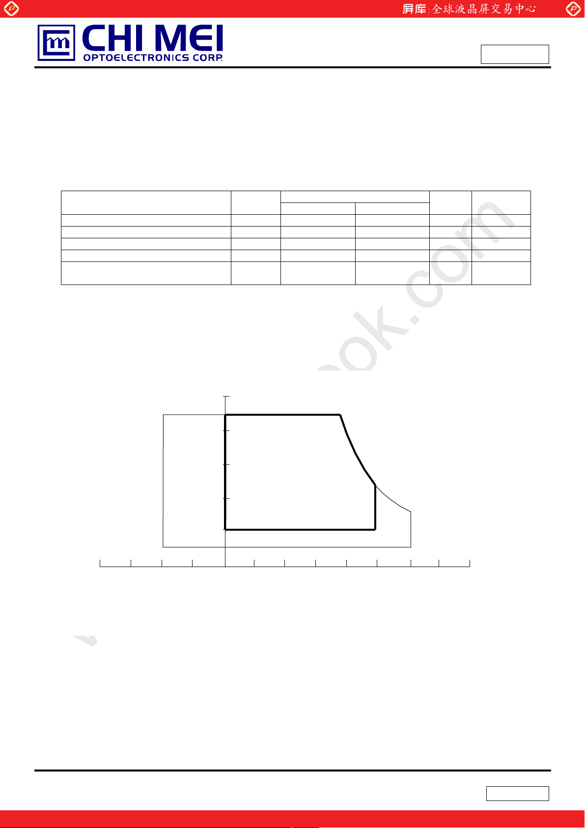
Note (1) Temperature and relative humidity range is shown in the figure below.
- 50 G (3), (5)
NOP
- 1 G (4), (5)
NOP
50,000 - Hrs
CELL
Min. Max.
Value
Unit Note
MTBF
based
(a) 90 %RH Max. (Ta Љ 40 ºC).
(b) Wet-bulb temperature should be 39 ºC Max. (Ta > 40 ºC).
(c) No condensation.
Relative Humidity (%RH)
100
90
80
60
Operating Range
40
20
10
Storage Range
80 60 -20 40 0 20 -40
Temperature (ºC)
Note (2) The temperature of panel display surface area should be 0 ºC Min. and 60 ºC Max.
Note (3) 11ms, half sine wave, 1 time for ± X, ± Y, ± Z.
Note (4) 10 ~ 300 Hz, 10min/cycle, 3 cycles each X, Y, Z.
Note (5) Upon the Vibration and Shock tests, the fixture used to hold the module must be firm and rigid
enough to prevent the module from twisting or bending by the fixture.
5 / 29
One step solution for LCD / PDP / OLED panel application: Datasheet, inventory and accessory!
Version 0.0
www.panelook.com
Page 6
Global LCD Panel Exchange Center
Issued Date: Mar. 12, 2008
www.panelook.com
DOC No.:
Model No.: S220Z1-M02
Ten tative
2.2 ELECTRICAL ABSOLUTE RATINGS
2.2.1 TFT LCD MODULE
Item Symbol
Power Supply Voltage for
LCD
Logic Input Voltage
Logic Input Voltage
Min. Max.
Vin
V5A
VDD
Value
Unit Note
V
V
V
(1)
Item Symbol
Power Supply Voltage Vcc -0.3 +5.5 V
Logic Input Voltage VIN -0.3 +4.3 V
Min. Max.
Value
Unit Note
(1)
2.2.2 BACKLIGHT UNIT
Item Symbol
Lamp Voltage V
Lamp Current IL 3.0 8.0 mA
Lamp Frequency FL 40 80 KHz
Note (1) Permanent damage to the device may occur if maximum values are exceeded. Function operation
should be restricted to the conditions described under Normal Operating Conditions.
Note (2) Specified values are for lamp (Refer to 3.2 for further information).
L
Min. Max.
Value
- 2.5K V
Unit Note
(1), (2), IL = 7.0mA
RMS
RMS
(1), (2)
6 / 29
One step solution for LCD / PDP / OLED panel application: Datasheet, inventory and accessory!
Version 0.0
www.panelook.com
Page 7
Global LCD Panel Exchange Center
Issued Date: Mar. 12, 2008
www.panelook.com
DOC No.:
Model No.: S220Z1-M02
Ten tative
3. ELECTRICAL CHARACTERISTICS
3.1 TFT LCD MODULE
Parameter SYMBOL
Power Supply Voltage for LCD Vin 12.42 13.8 15.18 V
Power Supply Current for LCD Iin 300 mA
Logic Input Voltage V5A 4.75 5 5.25 V
Logic Input Current I5A 0.5 A
Driver Logic Input Voltage VDD 3.135 3.3 3.465 V
Driver Logic Input Current IDD 60 mA
Differential Impendence Zm 100
High VIH 0.8VDD - VDD V Logic Input Voltage
Low VIL 0 - VDD V
LCD Inrush Current Irush 3 A
Power Consumption P 5 W
High 2.5 3.3 V MAX=3.6 is okPANE L On
Low
High 2.5 3.3 V MAX=3.6 is okDCDC On
Low
High VCOM_PWM 2.5 V MAX=5.45 is okVCOM PWM
Low 0.6 V
VCOM PWM Frequency VCOM_PWM 27 KHz Adjustable Duty
Ta = 25 ± 2 ºC
Parameter Symbol
Power Supply Voltage Vcc 4.5 5.0 5.5 V Ripple Voltage VRP - -- 250 mV Rush Current I
White - 630 819 mA (3)a
Power Supply Current
LVDS differential input voltage Vid 200 - 600 mV
LVDS common input voltage Vic -- 1.2 -- V
Above all conditions are VDD=5.0V, all black pattern at 75HZ.
Black - 1170 1521 mA (3)b
= 75Hz,
f
V
Vcc=4.5V
PANEL_ON
DCDC_ ON
Ta = 25 ± 2 ºC
Value
MIN TYP MAX
0.6 V
0.6 V
Value
Min. Typ. Max.
- -- 3 A (2)
RUSH
lcc
- 1330 1729 mA (4)
UNIT Note
Ө
(2)
Cycle
Unit Note
Note (1) The module should be always operated within above ranges.
Note (2) Measurement Conditions:
7 / 29
One step solution for LCD / PDP / OLED panel application: Datasheet, inventory and accessory!
Version 0.0
www.panelook.com
Page 8
Global LCD Panel Exchange Center
www.panelook.com
DOC No.:
Issued Date: Mar. 12, 2008
Model No.: S220Z1-M02
Ten tative
(High to Low)
(Control Signal)
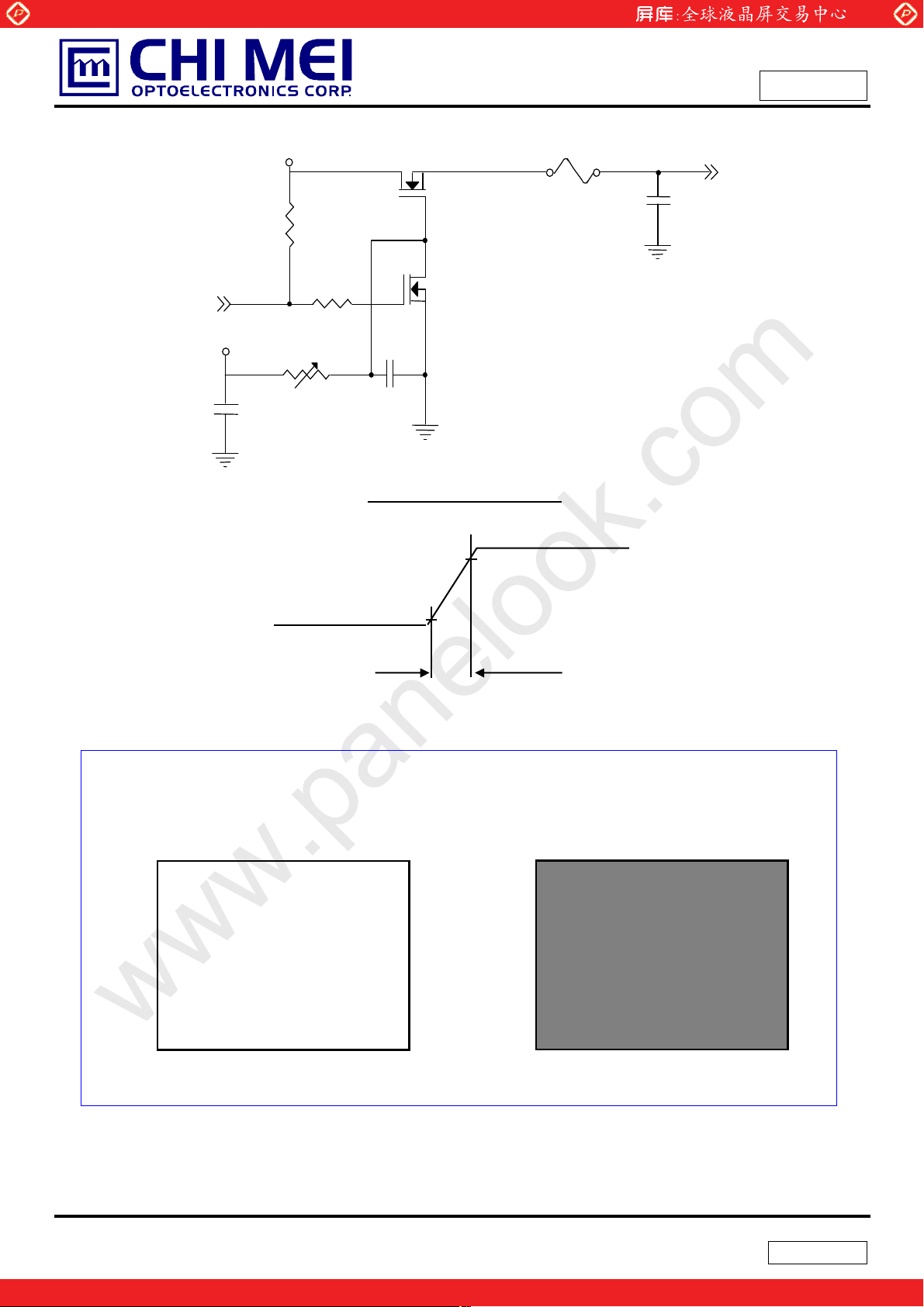
SW
+12V
+5.0V
R1
47K
R2
1K
47K
VR1
C1
1uF
Q1 2SK1475
C2
0.01uF
Q2
2SK1470
FUSE
C3
1uF
Vcc
(LCD Module Input)
Vcc rising time is 470s
+5.0V
0.9Vcc
0.1Vcc
GND
470s
Note (3) The specified power supply current is under the conditions at Vcc = 5.0 V, Ta = 25 ± 2 ºC, fv = 60
Hz, whereas a power dissipation check pattern below is displayed.
a. White Pattern
b. Black Pattern
Active Area
Active Area
8 / 29
One step solution for LCD / PDP / OLED panel application: Datasheet, inventory and accessory!
Version 0.0
www.panelook.com
Page 9
Global LCD Panel Exchange Center
Issued Date: Mar. 12, 2008
www.panelook.com
DOC No.:
Model No.: S220Z1-M02
Ten tative
c. Vertical Stripe Pattern
R
R
B
R
B
R R
Active Area
Note (3) The specified power supply current is under the conditions at Vcc = 5.0 V, Ta = 25 ± 2 ºC, fv = 60
Hz, whereas a power dissipation check pattern below is displayed.
a. White Pattern
b. Black Pattern
G
G
G
G
B
B
B
B
R
R
R
G
G
G
G
B
B
B
B
R
R
Active Area
Note (4) The specified power supply current is under the conditions at Vcc = 4.5 V, Ta = 25 ± 2 ºC, f
Hz, whereas a power dissipation check pattern (Black Pattern) below is displayed.
Black Pattern
Active Area
Active Area
= 75
v
9 / 29
One step solution for LCD / PDP / OLED panel application: Datasheet, inventory and accessory!
Version 0.0
www.panelook.com
Page 10
Global LCD Panel Exchange Center
www.panelook.com
DOC No.:
Issued Date: Mar. 12, 2008
Model No.: S220Z1-M02
Ten tative
3.2 BACKLIGHT UNIT
Parameter Symbol
Min. Typ. Max.
Lamp Input Voltage VL 738 820 902 V
Lamp Current IL 3 7.0 8 mA
Lamp Turn On Voltage V
S
- -
- -
Value
1560(25к)
1800(0к)
Ta = 25 ± 2 ºC
Unit Note
IL = 7.0 mA
RMS
RMS
V
(2)
RMS
V
(2)
RMS
(1)
Operating Frequency FL 40 60 80 KHz (3)
Lamp Life Time LBL 50000 - - Hrs (5), IL = 7.0 mA
Power Consumption PL - 22.96 - W (4), IL = 7.0 mA
Note (1) Lamp current is measured by utilizing high frequency current meters as shown below:
HV (Pink)
LV (White)
LCD
HV (Blue)
LV (Black)
1
2
A
Inverter
A
Current Meter
YOKOGAWA 2016
1
2
A
Note (2) The voltage that must be larger than Vs should be applied to the lamp for more than 1 second
after startup. Otherwise the lamp may not be turned on.
Note (3) The lamp frequency may produce interference with horizontal synchronous frequency from the
display, and this may cause line flow on the display. In order to avoid interference, the lamp
frequency should be detached from the horizontal synchronous frequency and its harmonics as far
as possible.
Note (4) P
= ILVL 4 CCFLs
L
Note (5) The lifetime of lamp can be defined as the time in which it continues to operate under the condition
Ta = 25 2
o
C and IL = 7.0 mA rms until one of the following events occurs:
(a) When the brightness becomes or lower than 50% of its original value.
(b) When the effective ignition length becomes or lower than 80% of its original value. (Effective
ignition length is defined as an area that has less than 70% brightness compared to the
brightness in the center point.)
Note (6) The waveform of the voltage output of inverter must be area-symmetric and the design of the
inverter must have specifications for the modularized lamp. The performance of the Backlight,
such as lifetime or brightness, is greatly influenced by the characteristics of the DC-AC inverter for
the lamp. All the parameters of an inverter should be carefully designed to avoid producing too
much current leakage from high voltage output of the inverter. When designing or ordering the
inverter please make sure that a poor lighting caused by the mismatch of the Backlight and the
inverter (miss-lighting, flicker, etc.) never occurs. If the above situation is confirmed, the module
should be operated in the same manners when it is installed in your instrument.
10 / 29
One step solution for LCD / PDP / OLED panel application: Datasheet, inventory and accessory!
Version 0.0
www.panelook.com
Page 11

Global LCD Panel Exchange Center
www.panelook.com
DOC No.:
Issued Date: Mar. 12, 2008
Model No.: S220Z1-M02
Ten tative
The output of the inverter must have symmetrical (negative and positive) voltage waveform and
symmetrical current waveform.(Unsymmetrical ratio is less than 10%) Please do not use the inverter
which has unsymmetrical voltage and unsymmetrical current and spike wave. Lamp frequency may
produce interface with horizontal synchronous frequency and as a result this may cause beat on the
display. Therefore lamp frequency shall be as away possible from the horizontal synchronous
frequency and from its harmonics in order to prevent interference.
Requirements for a system inverter design, which is intended to have a better display performance, a
better power efficiency and a more reliable lamp. It shall help increase the lamp lifetime and reduce its
leakage current.
a. The asymmetry rate of the inverter waveform should be 10% below;
b. The distortion rate of the waveform should be within Ѕ2 ± 10%;
c. The ideal sine wave form shall be symmetric in positive and negative polarities.
* Asymmetry rate:
I
p
I
-p
| I
– I –p | / I
p
* Distortion rate
I
(or I –p) / I
p
rms
rms
* 100%
11 / 29
One step solution for LCD / PDP / OLED panel application: Datasheet, inventory and accessory!
Version 0.0
www.panelook.com
Page 12

Global LCD Panel Exchange Center
R
www.panelook.com
DOC No.:
Issued Date: Mar. 12, 2008
Model No.: S220Z1-M02
Ten tative
4. BLOCK DIAGRAM
4.1 TFT LCD MODULE
RXO0(+/-)
RXO1(+/-)
RXO2(+/-)
RXO3(+/-)
RXOC(+/-)
RXE0(+/-)
RXE1(+/-)
RXE2(+/-)
RXE3(+/-)
RXEC(+/-)
AGMODE
Vcc
GND
(STARCONN 093G30-B0001A)
LVDS INPUT /
INPUT CONNECTOR
TIMING CONTROLLER
DC/DC CONVERTER &
REFERENCE VOLTAGE
SCAN DRIVER IC
TFT LCD PANEL
(1680x3x1050)
DATA DRIVER IC
V
L
LAMP CONNECTO
(YEONHO 35001HS-02L)
4.2 BACKLIGHT UNIT
BACKLIGHT UNIT
1 HV(Pink)
2 LV(White)
1 HV(Blue)
2 LV(Black)
1 HV(Pink)
2 LV(White)
1 HV(Blue)
Note: On the same side, the same-polarity lamp voltage design for lamps is recommended
12 / 29
One step solution for LCD / PDP / OLED panel application: Datasheet, inventory and accessory!
2 LV(Black)
Version 0.0
www.panelook.com
Page 13

Global LCD Panel Exchange Center
Issued Date: Mar. 12, 2008
www.panelook.com
DOC No.:
Model No.: S220Z1-M02
Ten tative
5. INPUT TERMINAL PIN ASSIGNMENT
5.1 TFT LCD MODULE
(1)CN1 (Panel Interface)
Pin Name Description
1 Vin Driver Power Input Voltage
2 Vin Driver Power Input Voltage
3 V5A
4 PANEL_ON
5 DCDC_ON
6 VCM_PWM
7 GVOFF Gate driver high voltage switch timing control.
8 NC No connect
9 GND Ground
10 BSTHI Data driver start pulse input(Back)
11 GND Ground
12 BR0N Negative RSDS differential data input. Channel R0(Back)
13 BR0P Positive RSDS differential data input. Channel R0(Back)
14 BR1N Negative RSDS differential data input. Channel R1(Back)
15 BR1P Positive RSDS differential data input. Channel R1(Back)
16 BR2N Negative RSDS differential data input. Channel R2(Back)
17 BR2P Positive RSDS differential data input. Channel R2(Back)
18 GND Ground
19 BCKN Negative RSDS differential clock input. (Back)
20 BCKP Positive RSDS differential clock input. (Back)
21 GND Ground
22 BG0N Negative RSDS differential data input. Channel G0(Back)
23 BG0P Positive RSDS differential data input. Channel G0(Back)
24 BG1N Negative RSDS differential data input. Channel G1(Back)
25 BG1P Positive RSDS differential data input. Channel G1(Back)
26 BG2N Negative RSDS differential data input. Channel G2(Back)
27 BG2P Positive RSDS differential data input. Channel G2(Back)
28 GND Ground
29 BB0N Negative RSDS differential data input. Channel B0(Back)
30 BB0P Positive RSDS differential data input. Channel B0(Back)
31 BB1N Negative RSDS differential data input. Channel B1(Back)
32 BB1P Positive RSDS differential data input. Channel B1(Back)
33 BB2N Negative RSDS differential data input. Channel B2(Back)
34 BB2P Positive RSDS differential data input. Channel B2(Back)
35 GND Ground
36 GND Ground
Logic Input Voltage +5V
This pin is used to control the driver
PANEL_ON
input is “H”, VDD will be to driver.
This pin is used to control the PWM IC. When
enable PWM IC.
This pin is used to generate common voltage for panel. Adjust pulse
width could be changed common voltage.
Logic Input Voltage VDD
DCDC_ON
input is “H”, it
. When
13 / 29
One step solution for LCD / PDP / OLED panel application: Datasheet, inventory and accessory!
Version 0.0
www.panelook.com
Page 14

Global LCD Panel Exchange Center
Issued Date: Mar. 12, 2008
www.panelook.com
DOC No.:
Model No.: S220Z1-M02
Ten tative
(2)CN1 (Panel Interface)
Pin Name Description
1 VDD Driver Logic Input Voltage
2 VDD Driver Logic Input Voltage
3 XAO
4 STV
5 CKV
6 OE
7 GND Ground
8 FR0N Negative RSDS differential data input. Channel R0(Front)
9 FR0P Positive RSDS differential data input. Channel R0(Front)
10 FR1N Negative RSDS differential data input. Channel R1(Front)
11 FR1P Positive RSDS differential data input. Channel R1(Front)
12 FR2N Negative RSDS differential data input. Channel R2(Front)
13 FR2P Positive RSDS differential data input. Channel R2(Front)
14 GND Ground
15 POL
16 STB
17 GND Ground
18 FCKN Negative RSDS differential clock input. (Front)
19 FCKP Positive RSDS differential clock input. (Front)
20 GND Ground
21 FG0N Negative RSDS differential data input. Channel G0(Front)
22 FG0P Positive RSDS differential data input. Channel G0(Front)
23 FG1N Negative RSDS differential data input. Channel G1(Front)
24 FG1P Positive RSDS differential data input. Channel G1(Front)
25 FG2N Negative RSDS differential data input. Channel G2(Front)
26 FG2P Positive RSDS differential data input. Channel G2(Front)
27 GND Ground
28 FB0N Negative RSDS differential data input. Channel B0(Front)
29 FB0P Positive RSDS differential data input. Channel B0(Front)
30 FB1N Negative RSDS differential data input. Channel B1(Front)
31 FB1P Positive RSDS differential data input. Channel B1(Front)
32 FB2N Negative RSDS differential data input. Channel B2(Front)
33 FB2P Positive RSDS differential data input. Channel B2(Front)
34 FSTHI Data driver start pulse input(Front)
35 GND Ground
36 GND Ground
Note (1) Connector Part No.: IL-FHR-F36S-HF.
When /XAO input pin is low, all the Gate driver output pins are forced to
VGH level. Note that this pin has higher priority than OE.
Gate driver start pulse is read at the rising edge of CKV and a scan
signal is output from the gate driver output pin.
Gate driver shift clock
This pin is used to control the Gate driver output. When OE input is “H”,
gate driver output is fixed to VGL level regardless CKV.
Data driver polarity inverting input
The contents of the data driver register are transferred to the latch circuit
at the rising edge of STB. Then the gray scale voltage is output from the
device at the falling edge of STB.
14 / 29
One step solution for LCD / PDP / OLED panel application: Datasheet, inventory and accessory!
Version 0.0
www.panelook.com
Page 15

Global LCD Panel Exchange Center
Issued Date: Mar. 12, 2008
www.panelook.com
DOC No.:
Model No.: S220Z1-M02
Ten tative
Pin Name Description
1 RXO0- Negative LVDS differential data input. Channel O0 (odd)
2 RXO0+ Positive LVDS differential data input. Channel O0 (odd)
3 RXO1- Negative LVDS differential data input. Channel O1 (odd)
4 RXO1+ Positive LVDS differential data input. Channel O1 (odd)
5 RXO2- Negative LVDS differential data input. Channel O2 (odd)
6 RXO2+ Positive LVDS differential data input. Channel O2 (odd)
7 GND Ground
8 RXOC- Negative LVDS differential clock input. (odd)
9 RXOC+ Positive LVDS differential clock input. (odd)
10 RXO3- Negative LVDS differential data input. Channel O3(odd)
11 RXO3+ Positive LVDS differential data input. Channel O3 (odd)
12 RXE0- Negative LVDS differential data input. Channel E0 (even)
13 RXE0+ Positive LVDS differential data input. Channel E0 (even)
14 GND Ground
15 RXE1- Negative LVDS differential data input. Channel E1 (even)
16 RXE1+ Positive LVDS differential data input. Channel E1 (even)
17 GND Ground
18 RXE2- Negative LVDS differential data input. Channel E2 (even)
19 RXE2+ Positive LVDS differential data input. Channel E2 (even)
20 RXEC- Negative LVDS differential clock input. (even)
21 RXEC+ Positive LVDS differential clock input. (even)
22 RXE3- Negative LVDS differential data input. Channel E3 (even)
23 RXE3+ Positive LVDS differential data input. Channel E3 (even)
24 GND Ground
25 NC Not connection, this pin should be open.
26 VCOM VCOM Control, should be open.
27 AGMODE AGMODE should be tied to ground or open.
28 VCC +5.0V power supply
29 VCC +5.0V power supply
30 VCC +5.0V power supply
Note (1) Connector Part No.: 093G30-B0001A(STARCONN) or FI-X30SSL-HF(JAE) or EQUIVALENT.
Note (2) Mating Connector Part No.:FI-X30H ; FI-X30C* ; FI-X30M* ; FI-X30HL(-T),FI-X30C*L(-T) [JAE]
Note (3) The first pixel is odd.
Note (4) Input signal of even and odd clock should be the same timing.
15 / 29
Version 0.0
One step solution for LCD / PDP / OLED panel application: Datasheet, inventory and accessory!
www.panelook.com
Page 16

Global LCD Panel Exchange Center
Issued Date: Mar. 12, 2008
www.panelook.com
DOC No.:
Model No.: S220Z1-M02
Ten tative
5.2 LVDS DATA MAPPING TABLE
LVDS Channel E0
LVDS Channel E1
LVDS Channel E2
LVDS Channel E3
LVDS Channel O0
LVDS Channel O1
LVDS Channel O2
LVDS Channel O3
LVDS output D7 D6 D4 D3 D2 D1 D0
Data order EG0 ER5 ER4 ER3 ER2 ER1 ER0
LVDS output D18 D15 D14 D13 D12 D9 D8
Data order EB1 EB0 EG5 EG4 EG3 EG2 EG1
LVDS output D26 D25 D24 D22 D21 D20 D19
Data order DE NA NA EB5 EB4 EB3 EB2
LVDS output D23 D17 D16 D11 D10 D5 D27
Data order NA EB7 EB6 EG7 EG6 ER7 ER6
LVDS output D7 D6 D4 D3 D2 D1 D0
Data order OG0 OR5 OR4 OR3 OR2 OR1 OR0
LVDS output D18 D15 D14 D13 D12 D9 D8
Data order OB1 OB0 OG5 OG4 OG3 OG2 OG1
LVDS output D26 D25 D24 D22 D21 D20 D19
Data order DE NA NA OB5 OB4 OB3 OB2
LVDS output D23 D17 D16 D11 D10 D5 D27
Data order NA OB7 OB6 OG7 OG6 OR7 OR6
5.2 BACKLIGHT UNIT
Pin Symbol Description Remark
1 HV High Voltage Pink
2 LV Low Voltage White
1 HV High Voltage Blue
2 LV Low Voltage Black
Note (1) Connector Part No.: JST-BHSR-02VS-1 or equivalent
Note (2) User’s connector Part No.: JST-SM02B-BHSS-1-TB (JST) or equivalent
5.3 COLOR DATA INPUT ASSIGNMENT
The brightness of each primary color (red, green and blue) is based on the 8-bit gray
scale data input for the color. The higher the binary input, the brighter the color. The table
below provides the assignment of color versus data input.
Data Signal
Basic
Colors
Color
Black
Red
Green
Blue
Cyan
Magenta
Yellow
White
R7 R6 R5 R4 R3 R2 R1 R0 G7 G6 G5 G4 G3 G2 G1 G0 B7 B6 B5 B4 B3 B2 B1 B0
0
0
1
1
0
0
0
0
0
0
1
1
1
1
1
1
Red Green Blue
0
0
0
0
0
0
0
0
0
0
0
0
0
0
0
0
0
0
0
1
1
1
1
1
1
0
0
0
0
0
0
0
0
0
0
0
0
0
0
0
0
0
0
0
1
1
1
1
1
1
1
1
0
0
0
0
0
0
0
0
0
0
0
0
0
0
0
0
0
0
0
1
1
1
1
1
0
0
0
0
0
0
1
1
1
1
1
1
1
1
1
1
1
1
1
1
1
1
1
1
1
0
0
0
0
0
0
0
0
1
1
1
1
1
1
1
1
1
1
1
1
1
1
1
1
1
1
1
0
0
0
0
0
1
1
1
1
1
1
1
1
1
1
1
1
1
1
1
1
1
1
1
16 / 29
0
0
0
0
0
0
0
0
0
1
1
1
1
1
1
1
1
1
0
0
0
1
1
1
One step solution for LCD / PDP / OLED panel application: Datasheet, inventory and accessory!
Version 0.0
www.panelook.com
Page 17

Global LCD Panel Exchange Center
Issued Date: Mar. 12, 2008
www.panelook.com
DOC No.:
Model No.: S220Z1-M02
Ten tative
Red(0) / Dark
Gray
Scale
Of
Red
Gray
Scale
Of
Green
Gray
Scale
Of
Blue
Note (1) 0: Low Level Voltage, 1: High Level Voltage
Red(1)
Red(2)
:
:
Red(253)
Red(254)
Red(255)
Green(0) / Dark
Green(1)
Green(2)
:
:
Green(253)
Green(254)
Green(255)
Blue(0) / Dark
Blue(1)
Blue(2)
:
:
Blue(253)
Blue(254)
Blue(255)
0
0
0
0
0
0
0
0
0
0
0
0
0
0
0
0
0
0
0
0
1
:
:
:
:
:
:
:
:
:
:
:
:
:
:
1
1
1
1
1
1
0
1
1
1
1
1
1
1
1
1
1
1
1
1
1
0
0
0
0
0
0
0
0
0
0
0
0
0
0
0
0
0
0
0
0
0
:
:
:
:
:
:
:
:
:
:
:
:
:
:
0
0
0
0
0
0
0
0
0
0
0
0
0
0
0
0
0
0
0
0
0
0
0
0
0
0
0
0
0
0
0
0
0
0
0
0
0
0
0
0
0
0
:
:
:
:
:
:
:
:
:
:
:
:
:
:
0
0
0
0
0
0
0
0
0
0
0
0
0
0
0
0
0
0
0
0
0
0
0
0
0
0
0
0
0
1
0
0
0
0
0
0
0
0
0
0
0
0
0
0
0
:
:
:
:
:
:
:
:
:
:
:
:
:
:
:
:
1
0
0
0
0
0
0
0
0
0
0
0
0
0
0
0
1
0
0
0
0
0
0
0
0
0
0
0
0
0
0
0
0
0
0
0
0
0
0
0
0
0
:
:
:
:
:
:
:
:
:
:
:
:
0
1
1
1
1
1
0
1
1
1
1
1
0
1
1
1
1
1
0
0
0
0
0
0
0
0
0
0
0
0
0
0
0
0
0
0
:
:
:
:
:
:
:
:
:
:
:
:
0
0
0
0
0
0
0
0
0
0
0
0
0
0
0
0
0
0
0
0
0
0
0
1
:
:
:
:
1
0
1
1
1
1
0
0
0
0
0
0
:
:
:
:
0
0
0
0
0
0
0
0
0
0
:
:
0
0
0
0
1
0
:
:
1
0
1
0
0
0
:
:
0
0
0
0
0
0
0
0
0
0
0
0
0
0
0
0
0
0
0
0
0
0
0
0
0
0
:
:
:
:
:
:
:
:
:
:
:
:
:
:
:
:
0
0
0
0
0
0
0
0
0
0
0
0
0
0
0
0
0
0
0
0
0
0
0
0
0
0
0
0
0
0
0
0
0
0
0
0
0
0
0
0
0
0
0
0
0
0
0
0
:
:
:
:
:
:
:
:
:
:
:
:
:
:
:
:
0
0
0
0
0
0
0
0
0
0
0
0
0
0
0
0
0
0
0
0
0
0
0
0
0
0
0
0
0
0
0
0
0
0
0
0
0
0
0
1
0
0
0
0
0
0
1
0
:
:
:
:
:
:
:
:
:
:
:
:
:
:
:
:
1
1
1
1
1
1
0
1
1
1
1
1
1
1
1
1
1
1
0
1
1
1
1
1
17 / 29
One step solution for LCD / PDP / OLED panel application: Datasheet, inventory and accessory!
Version 0.0
www.panelook.com
Page 18

Global LCD Panel Exchange Center
www.panelook.com
DOC No.:
Issued Date: Mar. 12, 2008
Model No.: S220Z1-M02
Ten tative
6. INTERFACE TIMING
6.1 INPUT SIGNAL TIMING SPECIFICATIONS
FCKP-FCKN/
BCKP-BCKN
FSTHI/BSTHI
BR0P-BR0N
D00
D01
D00
FR0P-FR0N
D01 D00
D01 D00 D01
BR1P-BR1N
FR1P-FR1N
BR2P-BR2N
FR2P-FR2N
BG0P-BG0N
FG0P-FG0N
BG1P-BG1N
FG1P-FG1N
BG2P-BG2N
FG2P-FG2N
BB0P-BB0N
FB0P-FB0N
BB0P-BB0N
FB0P-FB0N
D02
D04
D10
D12
D14
D20
D22
D03
D05
D11
D13
D15
D21
D23
D02
D04
D10
D12
D14
D20
D22
D03 D02
D05 D04
D11 D10
D13 D12
D15 D14
D21 D20
D23 D22
D03 D02 D03
D05 D04 D05
D11 D10 D11
D13 D12 D13
D15 D14 D15
D21 D20 D21
D23 D22 D23
BB0P-BB0N
FB0P-FB0N
1st Data
D25 D24
2nd Data
D25 D24 D25
3rd Data
D24
D25
D24
18 / 29
One step solution for LCD / PDP / OLED panel application: Datasheet, inventory and accessory!
Version 0.0
www.panelook.com
Page 19

Global LCD Panel Exchange Center
www.panelook.com
DOC No.:
Issued Date: Mar. 12, 2008
Model No.: S220Z1-M02
Ten tative
6.2 POWER ON/OFF SEQUENCE
To prevent a latch-up or DC operation of LCD module, the power on/off sequence should be as the
diagram below.
Parameter Symbol Condition
Panel On to DC/DC On t
DC/DC On to RSDS Data t
RSDS Data to BL_On t
RSDS Data Off to Panel Off t
ˣ˴˸˿ʳˢ
˗˖˂˗˖ʳˢ
˧˶
˕˟˲ˢˡ
Spec
Min. Typ. Max.
1
2
3
4
- 10 - -
- 40 50 60
- 100 200 -
- 80 100 120
Unit
mS
˄
˅
ˆ
ˇ
6.1 INPUT SIGNAL TIMING SPECIFICATIONS
The input signal timing specifications are shown as the following table and timing diagram.
Signal Item Symbol Min. Typ. Max. Unit Note
Frequency Fc 50 59.5 82 MHz -
LVDS Clock
LVDS Data
Vertical Active Display Term
Horizontal Active Display Term
NoteΚ(1) Because this module is operated by DE only mode, Hsync and Vsync input signals should be set
Period Tc 13.4 16.8 - ns
High Time Tch - 4/7 - Tc Low Time Tcl - 3/7 - Tc Setup Time Tlvs 600 - - ps Hold Time Tlvh 600 - - ps Frame Rate Fr 50 60 76 Hz Tv=Tvd+Tvb
Total Tv 1060 1080 1195 Th Display Tvd 1050 1050 1050 Th Blank Tvb Tv-Tvd 30 Tv-Tvd Th Total Th 890 920 1000 Tc Th=Thd+Thb
Display Thd 840 840 840 Tc Blank Thb Th-Thd 80 Th-Thd Tc -
to low logic level or ground. Otherwise, this module would operate abnormally.
19 / 29
One step solution for LCD / PDP / OLED panel application: Datasheet, inventory and accessory!
Version 0.0
www.panelook.com
Page 20

Global LCD Panel Exchange Center
Issued Date: Mar. 12, 2008
www.panelook.com
DOC No.:
Model No.: S220Z1-M02
Ten tative
INPUT SIGNAL TIMING DIAGRAM
20 / 29
One step solution for LCD / PDP / OLED panel application: Datasheet, inventory and accessory!
Version 0.0
www.panelook.com
Page 21

Global LCD Panel Exchange Center
www.panelook.com
DOC No.:
Issued Date: Mar. 12, 2008
Model No.: S220Z1-M02
Ten tative
6.2 POWER ON/OFF SEQUENCE
To prevent a latch-up or DC operation of LCD module, the power on/off sequence should follow the
conditions shown in the following diagram.
CC
Power Supply
0.9 V
0.9 V
CC
V
0.5 ms T1 10 ms
0 T
0 T
500ms T
2
50 ms
3
50 ms
CC
0V
4
Signals
0V
Backlight (Recommended)
450ms
T
90msT
5
6
0.1V
CC
T
1
T
2
Power On
50%
T
5
Power ON/OFF Sequence
VALI D
50%
T
6
T
3
Power Off
0.1V
DD
T
4
Note.
(1) The supply voltage of the external system for the module input should be the same as the definition of Vcc.
(2) Please apply the lamp voltage within the LCD operation range. When the backlight turns on before the LCD
operation of the LCD turns off, the display may, instantly, function abnormally.
(3) In case of
VCC
= off level, please keep the level of input signals on the low or keep a high impedance.
(4) T4 should be measured after the module has been fully discharged between power on/off periods.
(5) Interface signal shall not be kept at high impedance when the power is on.
21 / 29
One step solution for LCD / PDP / OLED panel application: Datasheet, inventory and accessory!
Version 0.0
www.panelook.com
Page 22

Global LCD Panel Exchange Center
www.panelook.com
DOC No.:
Issued Date: Mar. 12, 2008
Model No.: S220Z1-M02
Ten tative
7. Driver DC Characteristics
7.1 RSDS CHARACTERISTICS
(Ta = - 10 to +85 °C, VDD = 2.3 to 3.6 V, VDDA = 8. 0 to 13.5 V, VSSD = VSSA = 0V)
Parameter Symbol Condition Min. Typ. Max. Unit
RSDS high input
voltage
RSDS low input voltage V
RSDS common mode
input voltage range
RSDS input leakage
current
V
DIFFRSDS
DIFFRSDS
V
CMRSDS
V
V
V
CMRSDS
CMRSDS
DIFFRSDS
= + 1.2 V
= + 1.2 V
= + 200 mV
IDL DxxP, DxxN, CLKP, CLKN -10 - 10 µA
(1)
(1)
(2)
VSSD + 0.1 - VDDD - 1.2 V
100 200 -
- -200 - 100
mV
Note: (1) V
(2) V
CLKP-CLKN
CMRSDS
= (VCLKP + VCLKN) / 2 or V
DIFFRSDS
= VCLKP - VCLKN or V
CLKN
CLKP
DIFFRSDS
V
DIFFRSDS
V
DIFFRSDS
CMRSDS
= (VDxxP + VDxxN) / 2
= VDxxP – VDxxN
V
DIFFRSDS
V
DIFFRSDS
V
CMRSDS
GND
0V
22 / 29
One step solution for LCD / PDP / OLED panel application: Datasheet, inventory and accessory!
Version 0.0
www.panelook.com
Page 23

Global LCD Panel Exchange Center
Issued Date: Mar. 12, 2008
www.panelook.com
DOC No.:
Model No.: S220Z1-M02
Ten tative
7.2 Electrical Characteristics (VSSD=VSSA=0V)
Parameter Symbol Condition
RSDS input “Low”
Voltage
RSDS input “High”
Voltage
RSDS reference
voltage
Input “Low” voltage V
Input “High” voltage V
V
DIFFRSDS
V
DIFFRSDS
V
CMRSDS
DX[2:0]P,DX[2:0]N,
IL
IH
EIO1,EIO2,DIR,TP1,
Input leak current IL
Supply current
(In operation mode)
Supply current
(In stand-by mode)
Supply current
(In operation mode)
Supply current
(In stand-by mode)
Output current
Output Voltage
range
Output Voltage
deviation
Gamma impedance Rr
I
VDDD=3.6V - TBD
CCD1
I
VDDD=3.6V - TBD TBD mA
CCD2
I
VDDA=13.5V - TBD
CCA1
I
VDDA=13.5V - TBD TBD mA
CCA2
I
VOH
I
VOL
Vout=Vӫ1-1V
Vout=Vӫ10+1V
Vout OUT1~OUT432 VSSA+0.1
Vcho-dev
VDDA=13.5V
Dxx=0 to 63 Gray
Vӫ1~Vӫ5,Vӫ6~Vӫ10
CLKP,CLKN
POL
Spec
Min. Typ. Max.
Unit
- -200 - mV
- 200 - mV
VSSD+0.1 1.2 VDDD-1.2 V
GND - 0.2VDDD µA
0.8VDDD - VDDD µA
- - 10 µA
(1)
TBD
TBD
(1)(2)
mA
mA
- - -100 µA
- - 100 µA
-
-
0.5Typ 16820 1.5Typ
VDDA-0.1 V
5 10
mV
Ө
Note:
(1) Test condition: TP1= 20µs, CLK =54MHz, data pattern =1010….checkerboard pattern, Ta=25
(2) No load condition
к
23 / 29
One step solution for LCD / PDP / OLED panel application: Datasheet, inventory and accessory!
Version 0.0
www.panelook.com
Page 24

Global LCD Panel Exchange Center
)
)
%
%
Issued Date: Mar. 12, 2008
www.panelook.com
DOC No.:
Model No.: S220Z1-M02
Ten tative
8.Driver AC Characteristics
Parameter Symbol Condition
Clock pulse width t
Clock pulse low period t
Clock pulse high period t
Data setup time t
Data hold time t
Start pulse setup time t
Start pulse hold time t
Last data CLK to TP1 high
TP1 high to EIOn high t
POL to TP1 setup time t
TP1 to POL hold time t
CLK
CLK(L)
CLK(H)
SETUP1
HOLD1
SETUP2
HOLD2
t
TP1(H)
t
LAST
NEXT
POL-TP1
TP1-POL
Min. Typ. Max.
- 11 - - ns
- 5 - - ns
- 5 - - ns
- 2 - - ns
- 0 - - ns
- 1 - - ns
- 2 - - ns
- 1 - - CLKPTP1 high period
- 0 - - CLKP
- 6 - - CLKP
POL toggle to TP1 rising 3 - - ns
TP1 falling to POL toggle 2 - - ns
Spec
Unit
CLKP-CLKN
(RSDS)
D**P – D**N
(RSDS)
BSTHI
D**P – D**N
(RSDS)
CLKP-CLKN
t
CLK
t
LAST-2
t
CLK(L
t
HOLD2
LAST-1
Even Odd Even
t
CLK(H
LAST
Even
t
Odd
t
LAST
t
t
t
Invalid
80
20%
STB
t
t
-
t
TP1- POL
POL
24 / 29
One step solution for LCD / PDP / OLED panel application: Datasheet, inventory and accessory!
20
80%
Version 0.0
www.panelook.com
Page 25

Global LCD Panel Exchange Center
Issued Date: Mar. 12, 2008
www.panelook.com
DOC No.:
Model No.: S220Z1-M02
Ten tative
9.Vertical Timing
Parameter Symbol Condition
CKV period t
CKV pulse width t
OE pulse width t
/XAO pulse width t
Data setup time t
Data hold time t
OE to CKV time t
STB to CKV t
STB Pulse Width t
CKV to GVOFF t
GVOFF Pulse width t
Note 1:GVOFF,OE,STB frequency same as CKV
Note 2:Width of OE pulse should be according to vertical frequency.
Ex:2.4 µs with 75Hz V-Sync ; 3.0µs with 60Hz V-Sync.
Note 3 : GVOff is used to make 3-step wave form to avoid V-Through on panel.
Note 4 : OE is used to control VGH_P output to panel. When OE is “H” , VGH_P output to panel is fixed to
“L” regardless CKV.
CKV
, t
CKVH
CKVL
OE
WXAO
SU
HD
OE-CKV
STB-CKV
STB
CKV -GVOFF
GVOFF
50% duty cycle 2.5 - - µs
-0.5 µs
- 5 - - µs
- 1 - 3.5 µs Note2
- 6 - - µs
- 700 - - ns
-
0.5 µs
0 0 0 µs
0.5 µs
12.8 µs Note1
Min. Typ. Max.
700 - - ns
Spec
Unit Remark
˖˞˩
˦˧˩
ˢ˘
˦˧˕
˚˩ˢ˙˙
˦˨
ˢ˘ˀ˖˞˩
ˢ˘
˛˗
˦˧˕ˀ˖˞˩
˖˞˩ˀ˚˩ˢ˙˙
˖˞˩
˚˩ˢ˙˙
˖˞˩˛ ˖˞˩˟
ˈ˃ʸ
ˈ˃ʸ
ˈ˃ʸ
25 / 29
One step solution for LCD / PDP / OLED panel application: Datasheet, inventory and accessory!
Version 0.0
www.panelook.com
Page 26

Global LCD Panel Exchange Center
www.panelook.com
DOC No.:
Issued Date: Mar. 12, 2008
Model No.: S220Z1-M02
Ten tative
10. OPTICAL CHARACTERISTICS
10.1 TEST CONDITIONS
Item Symbol Value Unit
Ambient Temperature Ta
Ambient Humidity Ha
Supply Voltage V
CC
252
5010
5.0 V
Input Signal According to typical value in "3. ELECTRICAL CHARACTERISTICS"
Inverter Current I
Inverter Driving Frequency F
L
L
7.0 mA
61 KHz
Inverter Darfon VK.13165.101
10.2 OPTICAL SPECIFICATIONS
The relative measurement methods of optical characteristics are shown in 7.2. The following items should
be measured under the test conditions described in 7.1 and stable environment shown in Note (6).
Item Symbol Condition Min. Typ. Max. Unit Note
0.649
0.335
0.283
0.605
0.151
0.073
0.313
0.329
Typ +
0.03
Color
Chromaticity
Red
Green
Blue
White
Rx
Ry
Gx
Gy
Bx
By
Wx
Wy
=0, Y=0
x
CS-1000T
R=G=B=255
Grayscale
Typ –
0.03
o
C
%RH
(1), (5)
Center Luminance of White L
C
250 300 --- cd/m2(4), (5)
Contrast Ratio CR 700 1000 --- - (2), (6)
Response Time
White Variation
Viewing Angle
Horizontal
Vertical
T
R
T
F
W
x+
-
x
Y+
-
Y
x=0, Y=0
=0, Y=0
x
CR>10
--- 1.3 2.2 ms
--- 3.7 5.8 ms
--- 1.3 1.42 - (5), (6)
75
75
70
70
85 --85
80
80
---
---
---
Deg. (1), (5)
Note (1) Definition of Viewing Angle (x, y):
(3)
26 / 29
One step solution for LCD / PDP / OLED panel application: Datasheet, inventory and accessory!
Version 0.0
www.panelook.com
Page 27

Global LCD Panel Exchange Center
T
www.panelook.com
DOC No.:
Issued Date: Mar. 12, 2008
Model No.: S220Z1-M02
Ten tative
Normal
x = y = 0º
y- y
X- = 90º
x-
x
6 o’clock
y- = 90º
y-
Note (2) Definition of Contrast Ratio (CR):
The contrast ratio can be calculated by the following expression.
Contrast Ratio (CR) = L255 / L0
L255: Luminance of gray level 255
L 0: Luminance of gray level 0
CR = CR (5)
CR (X) is corresponding to the Contrast Ratio of the point X at Figure in Note (6).
x
12 o’clock direction
y+
y+ = 90º
x+
X+ = 90º
Note (3) Definition of Response Time (T
Gray Level
100%
90%
Optical
Response
10%
0%
255
66.67ms
R
T
R
, TF):
Gray Level 0
27 / 29
T
F
66.67m
Gray Level
255
ime
One step solution for LCD / PDP / OLED panel application: Datasheet, inventory and accessory!
Version 0.0
www.panelook.com
Page 28

Global LCD Panel Exchange Center
www.panelook.com
DOC No.:
Issued Date: Mar. 12, 2008
Model No.: S220Z1-M02
Ten tative
Note (4) Definition of Luminance of White (LC):
Measure the luminance of gray level 255 at center point
= L (5)
L
C
L (x) is corresponding to the luminance of the point X at Figure in Note (6).
Note (5) Measurement Setup:
The LCD module should be stabilized at given temperature for 20 minutes to avoid abrupt
temperature change during measuring. In order to stabilize the luminance, the measurement
should be executed after lighting Backlight for 20 minutes in a windless room.
LCD Module
LCD Panel
USB2000
Field of View = 2º
Center of the Screen
Note (6) Definition of White Variation (W):
Measure the luminance of gray level 255 at 9 points
W = Maximum [L (1) ~ L (9)] / Minimum [L (1) ~ L (9)]
D/10 D/2
Horizontal Line
CS-1000T
Light Shield Room
(Ambient Luminance < 2 lux)
D
D/10
1 3
4
2
: Test Point
5
6
X
X=1 to 9
W
W/10
W/2
Vertical Line
W/10
One step solution for LCD / PDP / OLED panel application: Datasheet, inventory and accessory!
7
8
9
Active Area
28 / 29
Version 0.0
www.panelook.com
Page 29

Global LCD Panel Exchange Center
Issued Date: Mar. 12, 2008
www.panelook.com
DOC No.:
Model No.: S220Z1-M02
Ten tative
11. PACKAGING
11.1 PACKING SPECIFICATIONS
(1) 6 LCD modules / 1 Box
(2) Box dimensions: 595(L) X 330 (W) X 440 (H) mm
(3) Weight: 17.3 Kg (6 modules per box)
11.2 PACKING METHOD
(1) Carton Packing should have no failure in the following reliability test items.
Test Item Test Conditions Note
ISTA STANDARD
Random, Frequency Range: 1 – 200 Hz
Vibration
Dropping Test 1 Angle, 3 Edge, 6 Face, 60cm Non Operation
Top & Bottom: 30 minutes (+Z), 10 min (-Z),
Right & Left: 10 minutes (X)
Back & Forth 10 minutes (Y)
Non Operation
Figure. 8-1 Packing method
29 / 29
One step solution for LCD / PDP / OLED panel application: Datasheet, inventory and accessory!
Version 0.0
www.panelook.com
Page 30

Global LCD Panel Exchange Center
Issued Date: Mar. 12, 2008
www.panelook.com
DOC No.:
Model No.: S220Z1-M02
Ten tative
For ocean shipping
For air transport
Figure. 8-2 Packing method
Figure. 8-3 Packing method
30 / 29
One step solution for LCD / PDP / OLED panel application: Datasheet, inventory and accessory!
Version 0.0
www.panelook.com
Page 31

Global LCD Panel Exchange Center
Issued Date: Mar. 12, 2008
www.panelook.com
DOC No.:
Model No.: S220Z1-M02
Ten tative
12. DEFINITION OF LABELS
12.1 CMO MODULE LABEL
The barcode nameplate is pasted on each module as illustration, and its definitions are as following explanation.
(a) Model Name: M220Z1-L03
(b) Revision: Rev. XX, for example: A0, A1… B1, B2… or C1, C2…etc.
(c) CMO barcode definition:
Serial ID: XX
Code Meaning Description
XX CMO internal use XX Revision Cover all the change
X CMO internal use -
XX CMO internal use -
YMD
L Product line # Line 1=1, Line 2=2, Line 3=3, …
NNNN Serial number Manufacturing sequence of product
(d) Customer’s barcode definition:
Serial ID: CM
Code Meaning Description
CM Supplier code CMO=CM
22Z13 Model number M220Z1-L03=22Z13
X
X Source driver IC code
X Gate driver IC code
XX Cell location Tainan, Taiwan=TN
L Cell line # 1~12=0~C
XX Module location Tainan, Taiwan=TN; Ningbo China=NP
L Module line # 1~12=0~C
YMD
NNNN Serial number By LCD supplier
-XX-X-XX-YMD-L-NNNN
Year, month, day Year: 2001=1, 2002=2, 2003=3, 2004=4…
Month: 1~12=1, 2, 3, ~, 9, A, B, C
Day: 1~31=1, 2, 3, ~, 9, A, B, C, ~, W, X, Y, exclude I, O, and U.
-22Z13-X-X-X-XX-L-XX-L-YMD-NNNN
Revision code ZBD, C1=A, C2=B, ….
Non ZBD, C1=1, C2=2, ….
Century=1, CLL=2, Demos=3, Epson=4, Fujitsu=5, Himax=6,
Hitachi=7, Hynix=8, LDI=9, Matsushita=A, NEC=B, Novatec=C,
OKI=D, Philips=E, Renasas=F, Samsung=G, Sanyo=H, Sharp=I,
TI=J, Topro=K, Toshiba=L, Windbond=M
Year, month, day Year: 2001=1, 2002=2, 2003=3, 2004=4…
Month: 1~12=1, 2, 3, ~, 9, A, B, C
Day: 1~31=1, 2, 3, ~, 9, A, B, C, ~, T, U, V
31 / 29
One step solution for LCD / PDP / OLED panel application: Datasheet, inventory and accessory!
Version 0.0
www.panelook.com
Page 32

Global LCD Panel Exchange Center
Issued Date: Mar. 12, 2008
www.panelook.com
DOC No.:
Model No.: S220Z1-M02
Ten tative
13. PRECAUTIONS
13.1 ASSEMBLY AND HANDLING PRECAUTIONS
(1) Do not apply rough force such as bending or twisting to the module during assembly.
(2) To assemble or install module into user’s system can be only in clean working areas. The dust and oil
may cause electrical short or worsen the polarizer.
(3) It’s not permitted to have pressure or impulse on the module because the LCD panel and Backlight will
be damaged.
(4) Always follow the correct power sequence when LCD module is connecting and operating. This can
prevent damage to the CMOS LSI chips during latch-up.
(5) Do not pull the I/F connector in or out while the module is operating.
(6) Do not disassemble the module.
(7) Use a soft dry cloth without chemicals for cleaning, because the surface of polarizer is very soft and
easily scratched.
(8) It is dangerous that moisture come into or contacted the LCD module, because moisture may damage
LCD module when it is operating.
(9) High temperature or humidity may reduce the performance of module. Please store LCD module within
the specified storage conditions.
(10) When ambient temperature is lower than 10ºC may reduce the display quality. For example, the
response time will become slowly, and the starting voltage of CCFL will be higher than room
temperature.
13.2 SAFETY PRECAUTIONS
(1) The startup voltage of Backlight is approximately 1000 Volts. It may cause electrical shock while
assembling with inverter. Do not disassemble the module or insert anything into the Backlight unit.
(2) If the liquid crystal material leaks from the panel, it should be kept away from the eyes or mouth. In
case of contact with hands, skin or clothes, it has to be washed away thoroughly with soap.
(3) After the module’s end of life, it is not harmful in case of normal operation and storage.
32 / 29
One step solution for LCD / PDP / OLED panel application: Datasheet, inventory and accessory!
Version 0.0
www.panelook.com
 Loading...