

Page 1
Global LCD Panel Exchange Center
ுழၴʳຝ
ᐉு
ߡۥ
ދป
MODEL NO.: R300M1
www.panelook.com
PRODUCT SPECIFICATION
ϭ Tentative Specification
ϭ Preliminary Specification
Ϯ Approval Specification
SUFFIX: L01
Customer:
APPROVED BY SIGNATURE
Name / Title
Note
Please return 1 copy for your confirmation with your
signature and comments.
ʳ
ʳ
ʳ
ʳ
2011-03-14
16:09:50 ʳ
Version 2.1 17th, Feb., 2011 1 / 29
The copyright belongs to CHIMEI InnoLux. Any unauthorized use is prohibited.
One step solution for LCD / PDP / OLED panel application: Datasheet, inventory and accessory!
APPL
ขጥʳ
yuhsiang.chang
(്/514-10922)ʳ
Directorʳ Acceptʳ
www.panelook.com
Page 2
Global LCD Panel Exchange Center
REVISION HISTORY ------------------------------------------------------- 3
1. GENERAL DESCRIPTION ------------------------------------------------------- 4
1.1 OVERVIEW
1.2 FEATURES
1.3 APPLICATION
1.4 GENERAL SPECIFICATION
1.5 MECHANICAL SPECIFICATION
2. ABSOLUTE MAXIMUM RATINGS ------------------------------------------------------- 5
2.1 ABSOLUTE RATINGS OF ENVIRONMENT
2.2 ELECTRICAL ABSOLUTE RATINGS
2.2.1 TFT LCD MODULE
2.2.2 BACKLIGHT UNIT
3. ELECTRICAL CHARACTERISTICS ------------------------------------------------------- 6
3.1 TFT LCD MODULE
3.2 BACKLIGHT UNIT
3.3 INVERTER ELECTRICAL CHARACTERISTCS
www.panelook.com
PRODUCT SPECIFICATION
CONTENTS
4. BLOCK DIAGRAM ------------------------------------------------------- 11
4.1 TFT LCD MODULE
4.2 BACKLIGHT UNIT
5. INPUT TERMINAL PIN ASSIGNMENT ------------------------------------------------------- 12
5.1 TFT LCD MODULE (CN1)
5.2 TFT LCD MODULE (CN2)
5.3 LVDS INPUT DATA ORDER
5.4 DC/DC CONNECTOR SIGNAL
5.5 INVERTER INPUT SIGNAL
5.6 COLOR DATA INPUT ASSIGNMENT
6. INTERFACE TIMING ------------------------------------------------------- 17
6.1 INPUT SIGNAL TIMING SPECIFICATION
6.2 POWER ON/OFF SEQUENCE
7. OPTICAL CHARACTERISTICS ------------------------------------------------------- 21
7.1 OPTICAL SPECIFICATION
7.2 IMAGE RETENTION
8. PACKAGING ------------------------------------------------------- 24
8.1 PACKING SPECIFICATION
8.2 PACKING METHOD
9. DEFINITION OF LABEL ------------------------------------------------------- 26
10. PRECAUTIONS ------------------------------------------------------- 27
10.1 ASSEMBLY AND HANDLING PRECAUTION
10.2 SAFETY PRECAUTION
11. MECHANICAL CHARACTERISTICS ------------------------------------------------------ 28
11.1 Front side
11.2 Rear side
Version 2.1 17th, Feb., 2011 2 / 29
The copyright belongs to CHIMEI InnoLux. Any unauthorized use is prohibited.
One step solution for LCD / PDP / OLED panel application: Datasheet, inventory and accessory!
www.panelook.com
Page 3
Global LCD Panel Exchange Center
www.panelook.com
PRODUCT SPECIFICATION
REVISION HISTORY
Version Date Section Description
Ver 2.0
Ver 2.1
Jan.3, ‘11
Feb.17,’11
All
2.2.2
3.2
3.3
4.1
5.5.1
5.5.2
R300M1-L01 Approval Specifications is first issued.
Max lamp current = 5.8mA
Note (1)(2) @ I
Lamp Input Voltage Typ 920V
Lamp Current Min. 4.8mA, Typ. 5.3mA, Max. 5.8mA
Note(5) I
Item2 Input current (@Vin=24V) Typ. 3.4A
Item3 Input power Typ. 81W, Max 98W
Item5 VDIM Output current control(MIN) Min. 3.0V, Max. 3.15V
Item8 Output current, VDIM=0V Min. 4.8mA, Typ. 5.3mA, Max 5.8mA
CN8 Inverter CONNECTOR SM14B-PH-SM6-K-TB(HF)
PIN12 Inverter On/Off control (5V: On, 0V:Off)
Note (1)Connector Part No.: SM14B-PH-SM6-K-TB (HF) (JST) or equivalent
Add Output Connector : CP042CP1MR0-NH (CVILUX) or equivalent
L
= 5.3mA
L
= 4.8 ~ 5.8 mArms
@ IL = 5.3 mA
RMS
Note (2) Figure update
6.1
Version 2.1 17th, Feb., 2011 3 / 29
The copyright belongs to CHIMEI InnoLux. Any unauthorized use is prohibited.
One step solution for LCD / PDP / OLED panel application: Datasheet, inventory and accessory!
www.panelook.com
Page 4
Global LCD Panel Exchange Center
1. GENERAL DESCRIPTION
1.1 OVERVIEW
R300M1-L01is a 30.0” TFT Liquid Crystal Display module with Backlight unit and two port 41 pins 2ch-LVDS
interface. This module supports 4096 x 2600 DQSXGA screen and can display grayscale driven by 10bit
drivers. The LCD module includes built-in inverter for Backlight.
1.2 FEATURES
- This specification applies to the Type 30.0” Monochrome TFT LCD Module Model R300M1-L01. This module
includes an inverter card for the backlight.
- The screen format is intended to support DQSXGA 4096(H) x 2600(V) resolution.
- Supported gray scale is 10-bits data per Uni-pixel
- All input signals are LVDS (Low Voltage Differential Signaling) interface.
www.panelook.com
PRODUCT SPECIFICATION
1.3 APPLICATION
- This module is design for a TFT LCD Medical Monitor style display unit.
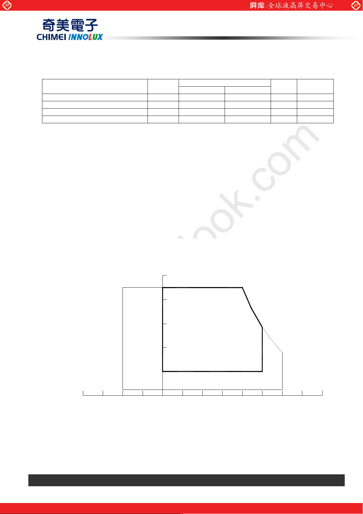
1.4 GENERAL SPECIFICATI0N
Item Specification Unit Note
Active Area 645.12 (H) x 403.2 (V) (30.0” diagonal) mm
Bezel Opening Area 649.2 (H) x 413.5 (V) mm
Driver Element a-si TFT active matrix - Pixel Number 4096 x 2600 pixel Pixel Pitch 0.158 (H) x 0.158 (V) mm Pixel Arrangement Uni-pixel - Display Colors 10-bits data per uni-pixel - Surface Treatment Hard coating (3H), Anti-glare (Haze 40) - -
(1)
1.5 MECHANICAL SPECIFICATION
Item Min. Typ. Max. Unit Note
Horizontal(H) 677.5 678.0 678.5 mm
Module Size
Note (1) Please refer to the attached drawings for more information of front and back outline dimensions.
Vertical(V) 447.5 448.0 448.5 mm
Depth(D) 48.5 49.0 49.5 mm
Weight 4600 -
(1)
Version 2.1 17th, Feb., 2011 4 / 29
The copyright belongs to CHIMEI InnoLux. Any unauthorized use is prohibited.
One step solution for LCD / PDP / OLED panel application: Datasheet, inventory and accessory!
www.panelook.com
Page 5
Global LCD Panel Exchange Center
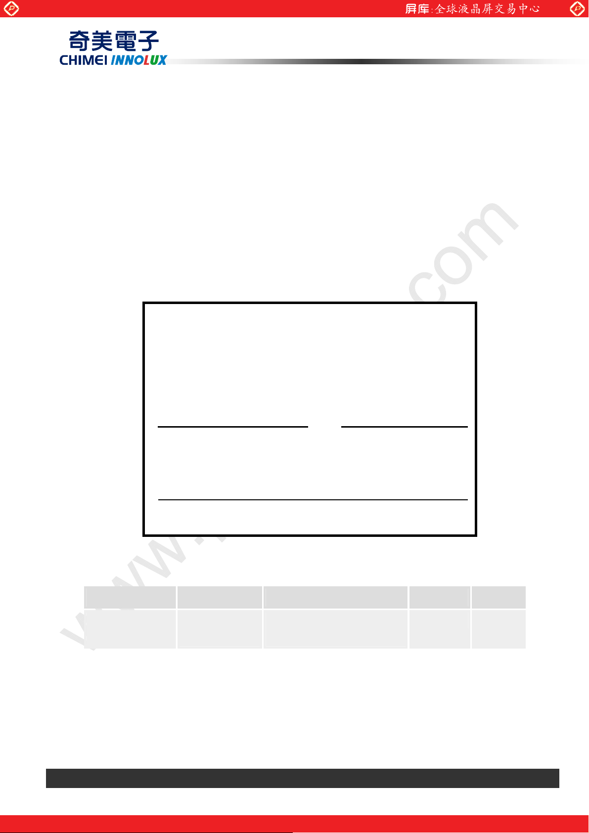
2. ABSOLUTE MAXIMUM RATINGS
2.1 ABSOLUTE RATINGS OF ENVIRONMENT
Item Symbol
Storage Temperature TST -20 +60 ºC (1)
Operating Ambient Temperature TOP 0 +50 ºC (1), (2)
Shock (Non-Operating) S
Vibration (Non-Operating) V
Note (1) Temperature and relative humidity range is shown in the figure below.
(a) 90 %RH Max. (Ta Љ 40 ºC).
(b) Wet-bulb temperature should be 39 ºC Max. (Ta > 40 ºC).
(c) No condensation.
www.panelook.com
PRODUCT SPECIFICATION
Min. Max.
NOP
NOP
- 50 G (3), (5)
- 1.5 G (4), (5)
Value
Unit Note
Note (2) The temperature of panel display surface area should be 0 ºC Min. and 60 ºC Max.
Note (3) 11ms, half sine wave, 1 time for ± X, ± Y, ± Z.
Note (4) 10 ~ 300 Hz, 10min/cycle, 3 cycles each X, Y, Z.
Note (5) At testing Vibration and Shock, the fixture in holding the module has to be hard and rigid enough so
that the module would not be twisted or bent by the fixture.
Relative Humidity (%RH)
100
90
80
6
Operating Range
40
2
10
-20 400 20 -40
Storage Range
6
Temperature (ºC)
Version 2.1 17th, Feb., 2011 5 / 29
The copyright belongs to CHIMEI InnoLux. Any unauthorized use is prohibited.
One step solution for LCD / PDP / OLED panel application: Datasheet, inventory and accessory!
80
www.panelook.com
Page 6

Global LCD Panel Exchange Center
2.2 ELECTRICAL ABSOLUTE RATINGS
2.2.1 TFT LCD MODULE
Item Symbol
Power Supply Voltage Vcc -0.3 +13.2 V
Logic Input Voltage V
2.2.2 BACKLIGHT UNIT
Item Symbol
Lamp Voltage VL - 1331 V
Lamp Current IL -5.8mA
Lamp Frequency FL - 80 KHz (1), (2)
Note (1) Permanent damage to the device may occur if maximum values are exceeded. Function operation
www.panelook.com
PRODUCT SPECIFICATION
Value
Min. Max.
-0.3 4 V
logic
Value
Min. Max.
Unit Note
Unit Note
RMS
RMS
(1)
(1), (2), IL =5.3mA
should be restricted to the conditions described under Normal Operating Conditions.
Note (2) Specified values are for lamp (Refer to 3.2 for further information).
3. ELECTRICAL CHARACTERISTICS
3.1.1 TFT LCD MODULE
Parameter Symbol
Power Supply Voltage Vcc 11.4 12.0 12.6 V (1)
Ripple Voltage VRP - - 100 mV (1)
Rush Current I
White - 0.82 1.148 A (3)a
Power Supply Current
Power Consumption P
Logic input high voltage V
Logic input low voltage V
LVDS differential input voltage Vid 100 - 600 mV
LVDS common input voltage Vic - 1.2 - V
Note (1) The module should be always operated within above ranges.
Black - 0.43 0.602 A (3)b
Vertical Stripe
Ta = 25 ± 2 ºC
Value
Min. Typ. Max.
- - 3.8 A (2)
RUSH
-
-
-
LCD
IH
IL
- 0.77 1.078 A (3)c
- 9.84 13.776 W (4)
2.64 - - V
- - 0.66 V
Unit Note
Version 2.1 17th, Feb., 2011 6 / 29
The copyright belongs to CHIMEI InnoLux. Any unauthorized use is prohibited.
One step solution for LCD / PDP / OLED panel application: Datasheet, inventory and accessory!
www.panelook.com
Page 7
Global LCD Panel Exchange Center
Note (2) Measurement Conditions:
www.panelook.com
PRODUCT SPECIFICATION
Note (3) The specified power supply current is under the conditions at Vcc = 12.0 V, Ta = 25 ± 2 ºC, fv = 50
Hz, whereas a power dissipation check pattern below is displayed.
a. White Pattern
Active Area
b. Black Pattern
Version 2.1 17th, Feb., 2011 7 / 29
The copyright belongs to CHIMEI InnoLux. Any unauthorized use is prohibited.
One step solution for LCD / PDP / OLED panel application: Datasheet, inventory and accessory!
www.panelook.com
Page 8
Global LCD Panel Exchange Center
www.panelook.com
PRODUCT SPECIFICATION
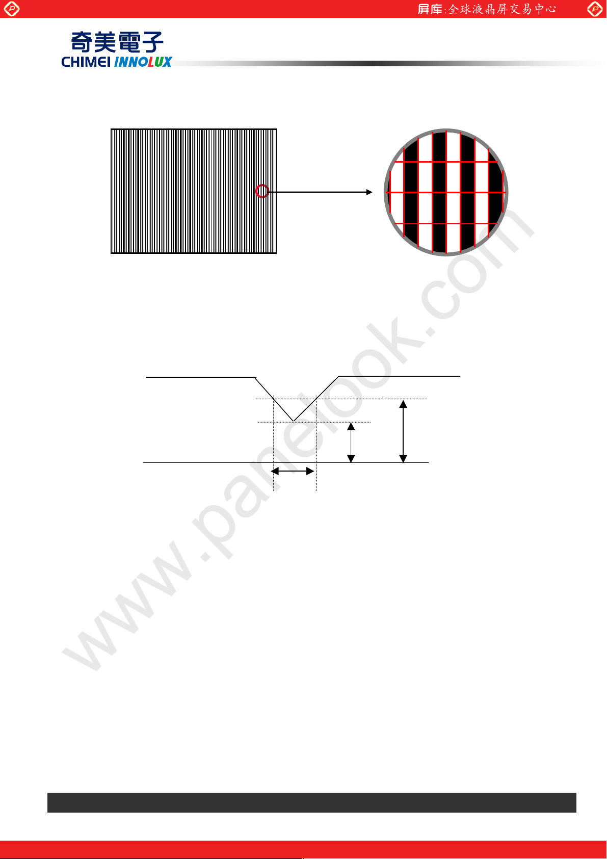
c. Vertical Stripe Pattern
B
B
Active Area
Note(4) The power consumption is specified at the pattern with the maximum current.
Active Area
A A
B
A
B
A
A A A
B B B
A A
A
A
B B
A A
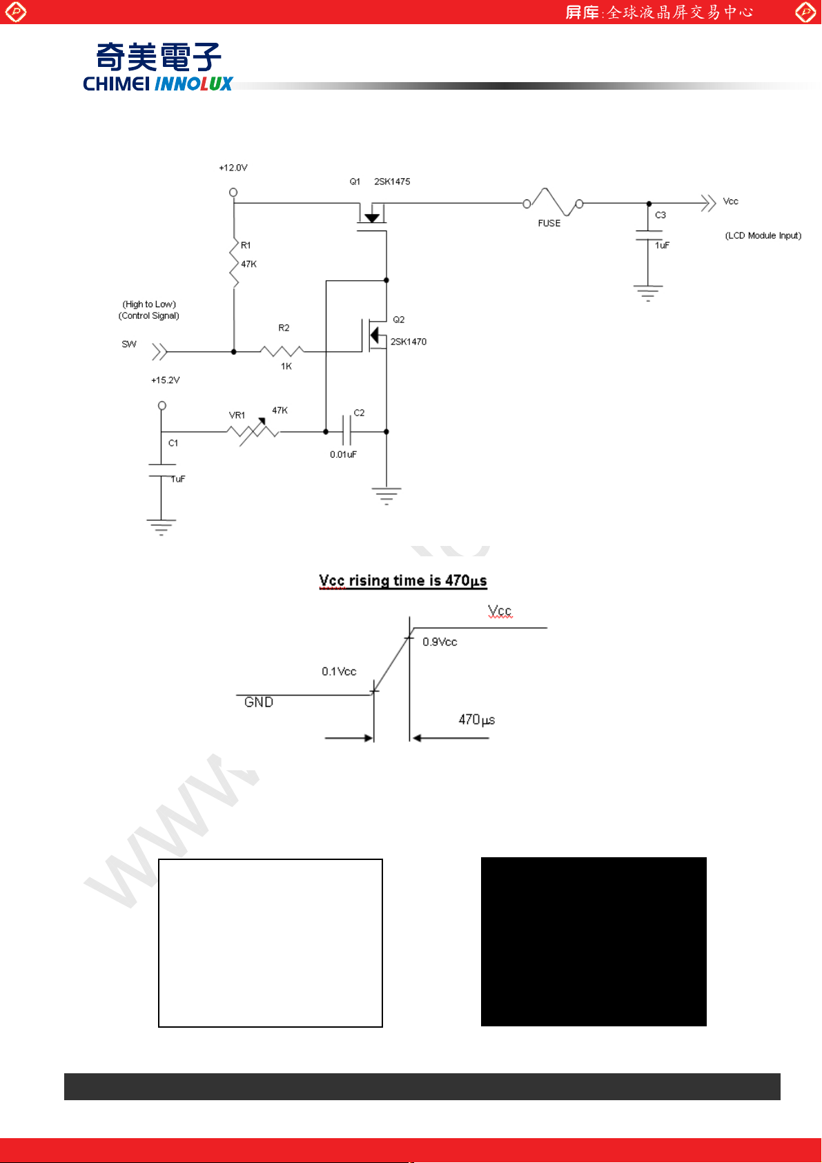
3.1.2 Vcc Power Dip Condition:
Vcc
B
B
B B
A
B
Dip condition:
11.1V
10
.2V
Td
msTdVVccV 20,1.112.10 ≤≤≤
Version 2.1 17th, Feb., 2011 8 / 29
The copyright belongs to CHIMEI InnoLux. Any unauthorized use is prohibited.
One step solution for LCD / PDP / OLED panel application: Datasheet, inventory and accessory!
www.panelook.com
Page 9
Global LCD Panel Exchange Center
)
)
)
www.panelook.com
PRODUCT SPECIFICATION
3.2 BACKLIGHT UNIT
Parameter Symbol
Min. Typ. Max.
Lamp Input Voltage VL - 920 - V
Lamp Current IL 4.8 5.3 5.8 mA
--- --- 1740(25 ºC) V
--- --- 2140(0 ºC) V
Voltage
V
S
Value
Ta = 25 ± 2 ºC
Unit Note
RMS
(IL = 5.3 mA)
(1)
(2) Lamp Turn On
(2)
RMS
RMS
RMS
Operating Frequency FL 37 40 43 KHz (3)
Lamp Life Time LBL 50,000 __ --- --- Hrs (5)
Note (1)Lamp current is measured by utilizing high frequency current meters as shown below:
HV (+
-
LCD
Module
ΗΗΗΗ
ΗΗΗΗ
Inverter
Current
Amplify
Oscilloscope
HV (+
HV (-
Current
Probe
Note (2) The voltage shown above should be applied to the lamp for more than 1 second after startup.
Otherwise the lamp may not be turned on.
Note (3) The lamp frequency may produce interference with horizontal synchronous frequency from the
display, and this may cause line flow on the display. In order to avoid interference, the lamp frequency
should be detached from the horizontal synchronous frequency and its harmonics as far as possible.
Note (4) P
= ILVL CCFLs
L
Note (5) The lifetime of lamp can be defined as the time in which it continues to operate under the condition
Ta = 25 2
o
C and IL = 4.8 ~ 5.8 mArms until one of the following events occurs:
(a)When the brightness becomes or lowers than 50% of its original value.
(b)When the effective ignition length becomes or lowers than 80% of its original value. (Effective ignition
length is defined as an area that has less than 70% brightness compared to the brightness in the center
point.)
Version 2.1 17th, Feb., 2011 9 / 29
The copyright belongs to CHIMEI InnoLux. Any unauthorized use is prohibited.
One step solution for LCD / PDP / OLED panel application: Datasheet, inventory and accessory!
www.panelook.com
Page 10

Global LCD Panel Exchange Center
3.3 Inverter Electrical characteristics
Ite
Symbol Description Min. Typ. Max. Unit
m
1 Vin Input voltage 22.8 24 25.2 V
2 Iin Input current (@Vin=24V) --- 3.4 --- A
3 Pin Input power --- 81 98 W
4 BLON Inverter On/Off control: OFF 0 --- 0.8 V
Inverter On/Off control: ON 2 --- 5 V
Output current control
5 VDIM
6 Fb Burst Mode Frequency 150 160 170 Hz
7 Freq. Operating frequency 37 40 43 KHz
VDIM: 0V, maximum brightness
VDIM: 3V, minimum brightness
www.panelook.com
PRODUCT SPECIFICATION
MAX --- 0 ---
V
MIN 3.0 --- 3.15
8 I
The following chart is the VDIM vs Dimming Range for your reference.
Output current, VDIM=0V 4.8 5.3 5.8 mA
out
Dimming Pipe
100%
80%
60%
40%
Dimming Duty
20%
0%
0
0.5
0.6
1.0
D
i
m
Wi
t
d
h
m
i
g
n
P
i
e
p
1.5 2.0
2.5 3.0
Dimming Voltage (V)
3.5
4.0
4.5
5.0
Version 2.1 17th, Feb., 2011 10 / 29
The copyright belongs to CHIMEI InnoLux. Any unauthorized use is prohibited.
One step solution for LCD / PDP / OLED panel application: Datasheet, inventory and accessory!
www.panelook.com
Page 11

Global LCD Panel Exchange Center
4. BLOCK DIAGRAM
4.1 TFT LCD MODULE
www.panelook.com
PRODUCT SPECIFICATION
RXinE0(+/-)
RXinE1(+/-)
RXinE2(+/-)
RECLKIN(+/-)
RXinE3(+/-)
RXinE4(+/-)
RXinO0(+/-)
RXinO1(+/-)
RXinO2(+/-)
ROCLKIN(+/-)
RXinO3(+/-)
RXinO4(+/-)
LVDS_SEL
Vcc
GND
(
JAE FI-RE41S-HF
)
(IL-Z-8PL-SMTYE)
J1/J2
CN1/CN2
LVDS INPUT /
TIMING ONTROLLER/
DC/DC CONVERTER &
REFERENCE VOLTAGE
SCAN DRIVER IC
TFTLCD PANEL
(4096x2600)
DATA DRIVERIC
Vin
GND
VDIM
BL_ON
<(SM14B-PH-SM6-K-TB(HF)>
4.2 BACKLIGHT UNIT
CN8
Inverter CONNECTOR
BACKLIGHT UNIT
1HV(Pink)
2HV(White)
ΖΖΖΖ
1HV(Pink)
2HV(White)
Version 2.1 17th, Feb., 2011 11 / 29
The copyright belongs to CHIMEI InnoLux. Any unauthorized use is prohibited.
One step solution for LCD / PDP / OLED panel application: Datasheet, inventory and accessory!
www.panelook.com
Page 12

Global LCD Panel Exchange Center
5. INPUT TERMINAL PIN ASSIGNMENT
5.1 CN1 (Master) : Left side (Front View)
Signal Description (CN1)
Pin Name Description
1 GND LVDS Ground
2 RXinE0- Negative LVDS differential data input. Channel E0 (even)
3 RXinE0+ Positive LVDS differential data input. Channel E0 (even)
4 RXinE1- Negative LVDS differential data input. Channel E1 (even)
5 RXinE1+ Positive LVDS differential data input. Channel E1 (even)
6 RXinE2- Negative LVDS differential data input. Channel E2 (even)
7 RXinE2+ Positive LVDS differential data input. Channel E2 (even)
8 GND LVDS Ground
9 RECLKIN- Negative LVDS differential clock input. (even)
10 RECLKIN+ Positive LVDS differential clock input. (even)
11 GND LVDS Ground
12 RXinE3- Negative LVDS differential data input. Channel E3 (even)
13 RXinE3+ Positive LVDS differential data input. Channel E3 (even)
14 RXinE4- Negative LVDS differential data input. Channel E4 (even)
15 RXinE4- Positive LVDS differential data input. Channel E4 (even)
16 GND LVDS Ground
17 RXinO0- Negative LVDS differential data input. Channel O0 (odd)
18 RXinO0+ Positive LVDS differential data input. Channel O0 (odd)
19 RXinO1- Negative LVDS differential data input. Channel O1 (odd)
20 RXinO1+ Positive LVDS differential data input. Channel O1 (odd)
21 RXinO2- Negative LVDS differential data input. Channel O2 (odd)
22 RXinO2+ Positive LVDS differential data input. Channel O2 (odd)
23 GND LVDS Ground
24 ROCLKIN- Negative LVDS differential clock input. (odd)
25 ROCLKIN+ Positive LVDS differential clock input. (odd)
26 GND LVDS Ground
27 RXinO3- Negative LVDS differential data input. Channel O3 (odd)
28 RXinO3+ Positive LVDS differential data input. Channel O3 (odd)
29 RXinO4- Negative LVDS differential data input. Channel O4 (odd)
30 RXinO4+ Positive LVDS differential data input. Channel O4 (odd)
31 GND LVDS Ground
32 GND Digital Ground
33 NC Not connection should keep open.
34 LVDS_SEL LVDS Input Date Order Selection( 0V:VESA, 3.3V:JEITA)
35 NC Not connection should keep open.
36 NC Not connection should keep open.
37 NC Not connection should keep open.
38 NC Not connection should keep open.
39 NC Not connection should keep open.
40 NC Not connection should keep open.
41 NC Not connection should keep open.
www.panelook.com
PRODUCT SPECIFICATION
Version 2.1 17th, Feb., 2011 12 / 29
The copyright belongs to CHIMEI InnoLux. Any unauthorized use is prohibited.
One step solution for LCD / PDP / OLED panel application: Datasheet, inventory and accessory!
www.panelook.com
Page 13

Global LCD Panel Exchange Center
5.2 CN2(Slave) : Right side(Front View)
Signal Description (CN2)
Pin Name Description
1 GND LVDS Ground
2 RXinE0- Negative LVDS differential data input. Channel E0 (even)
3 RXinE0+ Positive LVDS differential data input. Channel E0 (even)
4 RXinE1- Negative LVDS differential data input. Channel E1 (even)
5 RXinE1+ Positive LVDS differential data input. Channel E1 (even)
6 RXinE2- Negative LVDS differential data input. Channel E2 (even)
7 RXinE2+ Positive LVDS differential data input. Channel E2 (even)
8 GND LVDS Ground
9 RECLKIN- Negative LVDS differential clock input. (even)
10 RECLKIN+ Positive LVDS differential clock input. (even)
11 GND LVDS Ground
12 RXinE3- Negative LVDS differential data input. Channel E3 (even)
13 RXinE3+ Positive LVDS differential data input. Channel E3 (even)
14 RXinE4- Negative LVDS differential data input. Channel E4 (even)
15 RXinE4- Positive LVDS differential data input. Channel E4 (even)
16 GND LVDS Ground
17 RXinO0- Negative LVDS differential data input. Channel O0 (odd)
18 RXinO0+ Positive LVDS differential data input. Channel O0 (odd)
19 RXinO1- Negative LVDS differential data input. Channel O1 (odd)
20 RXinO1+ Positive LVDS differential data input. Channel O1 (odd)
21 RXinO2- Negative LVDS differential data input. Channel O2 (odd)
22 RXinO2+ Positive LVDS differential data input. Channel O2 (odd)
23 GND LVDS Ground
24 ROCLKIN- Negative LVDS differential clock input. (odd)
25 ROCLKIN+ Positive LVDS differential clock input. (odd)
26 GND LVDS Ground
27 RXinO3- Negative LVDS differential data input. Channel O3 (odd)
28 RXinO3+ Positive LVDS differential data input. Channel O3 (odd)
29 RXinO4- Negative LVDS differential data input. Channel O4 (odd)
30 RXinO4+ Positive LVDS differential data input. Channel O4 (odd)
31 GND LVDS Ground
32 GND Digital Ground
33 NC Not connection should keep open.
34 LVDS_SEL LVDS Input Date Order Selection( 0V:VESA, 3.3V:JEITA)
35 NC Not connection should keep open.
36 NC Not connection should keep open.
37 NC Not connection should keep open.
38 NC Not connection should keep open.
39 NC Not connection should keep open.
40 NC Not connection should keep open.
41 NC Not connection should keep open.
Note (1) Connector Part No.: FI-RE41S-HF (JAE) or equivalent.
www.panelook.com
PRODUCT SPECIFICATION
Note (2) User’s connector Part No.: FI-RE41HL (JAE).
Note (3) The first pixel is even.
Note (4) Input signal of even and odd clock should be the same timing.
Note (5) The module uses a 100-ohm resistor between positive and negative data lines of each receiver input
Version 2.1 17th, Feb., 2011 13 / 29
The copyright belongs to CHIMEI InnoLux. Any unauthorized use is prohibited.
One step solution for LCD / PDP / OLED panel application: Datasheet, inventory and accessory!
www.panelook.com
Page 14

Global LCD Panel Exchange Center
5.3 LVDS Input Data Order
VESA mode: LVDS_SEL=L (0V)
LVDS interface receiver required input data mapping table
LVDS Channel E0
LVDS Channel E1
LVDS Channel E2
LVDS Channel E3
LVDS Channel E4
LVDS Channel O0
LVDS Channel O1
LVDS Channel O2
LVDS Channel O3
LVDS Channel O4
LVDS output TA6 TA5 TA4 TA3 TA2 TA1 TA0
Data order EB0 EA5 EA4 EA3 EA2 EA1 EA0
LVDS output TB6 TB5 TB4 TB3 TB2 TB1 TB0
Data order EC1 EC0 EB5 EB4 EB3 EB2 EB1
LVDS output TC6 TC5 TC4 TC3 TC2 TC1 TC0
Data order DE NA NA EC5 EC4 EC3 EC2
LVDS output TD6 TD5 TD4 TD3 TD2 TD1 TD0
Data order NA EC7 EC6 EB7 EB6 EA7 EA6
LVDS output TE6 TE5 TE4 TE3 TE2 TE1 TE0
Data order NA EC9 EC8 EB9 EB8 EA9 EA8
LVDS output TA6 TA5 TA4 TA3 TA2 TA1 TA0
Data order OB0 OA5 OA4 OA3 OA2 OA1 OA0
LVDS output TB6 TB5 TB4 TB3 TB2 TB1 TB0
Data order OC1 OC0 OB5 OB4 OB3 OB2 OB1
LVDS output TC6 TC5 TC4 TC3 TC2 TC1 TC0
Data order DE NA NA OC5 OC4 OC3 OC2
LVDS output TD6 TD5 TD4 TD3 TD2 TD1 TD0
Data order NA OC7 OC6 OB7 OB6 OA7 OA6
LVDS output TE6 TE5 TE4 TE3 TE2 TE1 TE0
Data order NA OC9 OC8 OB9 OB8 OA9 OA8
www.panelook.com
PRODUCT SPECIFICATION
JEITA mode: LVDS_SEL=H (3.3V)
LVDS interface receiver required input data mapping table
LVDS Channel E0
LVDS Channel E1
LVDS Channel E2
LVDS Channel E3
LVDS Channel E4
LVDS Channel O0
LVDS Channel O1
LVDS Channel O2
LVDS Channel O3
LVDS Channel O4
LVDS output TA6 TA5 TA4 TA3 TA2 TA1 TA0
Data order EB4 EA9 EA8 EA7 EA6 EA5 EA4
LVDS output TB6 TB5 TB4 TB3 TB2 TB1 TB0
Data order EC5 EC4 EB9 EB8 EB7 EB6 EB5
LVDS output TC6 TC5 TC4 TC3 TC2 TC1 TC0
Data order DE NA NA EC9 EC8 EC7 EC6
LVDS output TD6 TD5 TD4 TD3 TD2 TD1 TD0
Data order NA EC3 EC2 EB3 EB2 EA3 EA2
LVDS output TE6 TE5 TE4 TE3 TE2 TE1 TE0
Data order NA EC1 EC0 EB1 EB0 EA1 EA0
LVDS output TA6 TA5 TA4 TA3 TA2 TA1 TA0
Data order OB4 OA9 OA8 OA7 OA6 OA5 OA4
LVDS output TB6 TB5 TB4 TB3 TB2 TB1 TB0
Data order OC5 OC4 OB9 OB8 OB7 OB6 OB5
LVDS output TC6 TC5 TC4 TC3 TC2 TC1 TC0
Data order DE NA NA OC9 OC8 OC7 OC6
LVDS output TD6 TD5 TD4 TD3 TD2 TD1 TD0
Data order NA OC3 OC2 OB3 OB2 OA3 OA2
LVDS output TE6 TE5 TE4 TE3 TE2 TE1 TE0
Data order NA OC1 OC0 OB1 OB0 OA1 OA0
Version 2.1 17th, Feb., 2011 14 / 29
The copyright belongs to CHIMEI InnoLux. Any unauthorized use is prohibited.
One step solution for LCD / PDP / OLED panel application: Datasheet, inventory and accessory!
www.panelook.com
Page 15

Global LCD Panel Exchange Center
5.4 DC/DC Connector Signal (J1/J2)
Pin No. Symbol Description
1-4 GND Ground for Vcc line
5-8 Vcc +12.0V Power Supply for Control board
Note (1) Connector Part No.: IL-Z-8PL-SMTYE (JAE) or equivalent
Note (2) User’s connector Part No.: IL-Z-8S-S125C3 (JAE)
5.5.1 Inverter Input Signal(CN8)
Pin No. Symbol Description
1 Vin Input voltage
2 Vin Input voltage
3 Vin Input voltage
4 Vin Input voltage
5 Vin Input voltage
6 GND Ground
7 GND Ground
8 GND Ground
9 GND Ground
10 GND Ground
11 VDIM Brightness control (0~3V)
12 BLON Inverter On/Off control (5V: On, 0V:Off)
13 NC No Connection
14 NC No Connection
Note (1) Connector Part No.:
www.panelook.com
PRODUCT SPECIFICATION
SM14B-PH-SM6-K-TB (HF)
(JST) or equivalent
Note (2) User’s connector Part No.: PHR-14-BK (JST)
5.5.2 Inverter Output Connector
Output Connector
Pin No. Symbol Description
1
2
: CP042CP1MR0-NH (CVILUX) or equivalent
CCFL HOT
CCFL HOT
CCFL high voltage
CCFL high voltage
Version 2.1 17th, Feb., 2011 15 / 29
The copyright belongs to CHIMEI InnoLux. Any unauthorized use is prohibited.
One step solution for LCD / PDP / OLED panel application: Datasheet, inventory and accessory!
www.panelook.com
Page 16

Global LCD Panel Exchange Center
A
A
A
A
A
A
A
A
5.6 Pixel Format Image
LVDS-LE LVDS-LO LVDS-RE LVDS-RO
www.panelook.com
PRODUCT SPECIFICATION
0 1 2 20482049 40951
3 4 5 2050205120522053
Left Screen
Right Screen
Active Area
2560
2561
BM (V16)
Non-Active Area : sensor area (V24)
2600
Following figure shows the relationship between the input signals and the LCD pixel format image. Each Even
pixel data and the right adjacent Odd pixel unit are sampled at the same time.
Pixel Arrangment
0 1
1th Line
2600th Line
2 3 4092 4093 4094 4095
BC
BC
BC
BC
Version 2.1 17th, Feb., 2011 16 / 29
The copyright belongs to CHIMEI InnoLux. Any unauthorized use is prohibited.
One step solution for LCD / PDP / OLED panel application: Datasheet, inventory and accessory!
www.panelook.com
Page 17

Global LCD Panel Exchange Center
T
T
T
T
6. INTERFACE TIMING
6.1 INPUT SIGNAL TIMING SPECIFICATION
The input signal timing specifications are shown as the following table and timing diagram.
Signal Item Symbol Min. Typ. Max. Unit Note
LVDS Cloc k
LVDS Data
Vertical Active Display Term
Horizontal Active Display Term
Note: Because this module is operated by DE only mode, Hsync and Vsync input signals are ignored.
www.panelook.com
PRODUCT SPECIFICATION
Frequency
clkin
F
Period Tc 18.97 19.54 20.15 ns
Input cycle to
cycle jitter
T
Spread
spectrum
modulation
clkin_mod
F
range
Spread
spectrum
modulation
F
SSM
frequency
High Time Tch - 4/7 - Tc Low Time Tcl - 3/7 - Tc Setup Time Tlvs 600 - - ps
Hold Time Tlvh 600 - - ps
Frame Rate Fr - 50 - Hz Total Tv 2615 2624 2650 Th Tv=Tvd+Tvb
Display Tvd 2600 2600 2600 Th Blank Tvb Tv-Tvd 24 Tv-Tvd Th Total Th 370 390 400 Tc Th=Thd+Thb
Display Thd 342 342 342 Tc Blank Thb Th-Thd 48 Th-Thd Tc -
48.37 51.17 53.00 MHz
360 ps (1)
rcl
-3 - 3 %
- - 300 KHz
(2)
(3)
DE
DCLK
DE
DATA
INPUT SIGNAL TIMING DIAGRAM
T
v
T
vd
h
C
hb
T
Vb
hd
Version 2.1 17th, Feb., 2011
The copyright belongs to CHIMEI InnoLux. Any unauthorized use is prohibited.
One step solution for LCD / PDP / OLED panel application: Datasheet, inventory and accessory!
17 / 29
www.panelook.com
Page 18

Global LCD Panel Exchange Center
Note (1) The input clock cycle-to-cycle jitter is defined as below figures. Trcl = I T1 – TI, Trcl = I T2 – TI
www.panelook.com
PRODUCT SPECIFICATION
T
1
Note (2) The SSCG (Spread spectrum clock generator) is defined as below figures.
T
2
Note (3) The LVDS timing diagram and setup/hold time is defined and showing as the following figures.
Version 2.1 17th, Feb., 2011
The copyright belongs to CHIMEI InnoLux. Any unauthorized use is prohibited.
18 / 29
One step solution for LCD / PDP / OLED panel application: Datasheet, inventory and accessory!
www.panelook.com
Page 19

Global LCD Panel Exchange Center
6.2 POWER ON/OFF SEQUENCE
To prevent a latch-up or DC operation of LCD module, the inverter power on and signal power on/off sequence
should be as the diagram below.
www.panelook.com
PRODUCT SPECIFICATION
Specifications:
0.5< t1 Љ 10 msec
0< t2 Љ 50 msec
0< t5 Љ 50 msec
t7 Њ 500 msec
t3 Њ 450 msec
t4 Њ 90 msec
5Љ t6 Љ 100 msec
n
T2
Timing Specifications:
TBL Њ 10 msec
Version 2.1 17th, Feb., 2011
The copyright belongs to CHIMEI InnoLux. Any unauthorized use is prohibited.
One step solution for LCD / PDP / OLED panel application: Datasheet, inventory and accessory!
19 / 29
www.panelook.com
Page 20

Global LCD Panel Exchange Center
Note(1) The supply voltage of the external system for the module input should be the same as the definition
of Vcc.
Note(2) Apply the lamp voltage within the LCD operation range. When the backlight turns on before the LCD
operation or the LCD turns off before the backlight turns off, the display may momentarily become
abnormal screen.
Note(3) In case of VCC = off level, please keep the level of input signals on the low or keep a high impedance.
Note(4) T4 should be measured after the module has been fully discharged between power off and on period.
www.panelook.com
PRODUCT SPECIFICATION
Note(5) Interface signal shall not be kept at high impedance when the power is on.
Version 2.1 17th, Feb., 2011
The copyright belongs to CHIMEI InnoLux. Any unauthorized use is prohibited.
One step solution for LCD / PDP / OLED panel application: Datasheet, inventory and accessory!
20 / 29
www.panelook.com
Page 21

Global LCD Panel Exchange Center
7. OPTICAL CHARACTERISTICS
7.1 OPTICAL SPECIFICATION
The relative measurement methods of optical characteristics are shown in 7.1. The following items should be
measured under the test conditions described in 7.1 and stable environment shown in Note (5).
Item Symbol Condition Min. Typ. Max. Unit Note
Color
Chromaticity
Center Luminance of White L
Contrast Ratio CR
Response Time
White Variation
Viewing Angle
White
Horizontal
Ver t ical
www.panelook.com
PRODUCT SPECIFICATION
Wx
Wy
C
θ
=0°, θY =0°
x
CS-1000
Typ –
0.03
1000 1250 - cd/m2(4), (5)
800 - - - (2), (5)
TR - 20 25 ms
T
F
δW
θx=0°, θY =0°
=0°, θY =0°
θ
x
USB2000
θx+
-
θ
x
θY+
θ
-
Y
CR Њ 10
USB2000
0.294
0.309
- 15 20 ms
Typ +
0.03
(1), (5)
(3)
- 1.25 1.4 - (5), (6)
80 85 80
80
80
85 85 -
Deg. (1), (5)
85 -
Note (1)Definition of Viewing Angle (θx, θy):
θX- = 90º
6 o’clock
θ
y-
= 90º
x-
y-
Note (2) Definition of Contrast Ratio (CR):
The contrast ratio can be calculated by the following expression.
Normal
θx = θy = 0º
θy- θy+
θx−
θx+
12 o’clock direction
y+
θ
y+
= 90º
x+
θX+ = 90º
Contrast Ratio (CR) = L1023 / L0
L1023: Luminance of gray level 1023
L 0: Luminance of gray level 0
CR = CR (x)
CR (X) is corresponding to the Contrast Ratio of the point X at Figure in Note (6).
Version 2.1 17th, Feb., 2011
The copyright belongs to CHIMEI InnoLux. Any unauthorized use is prohibited.
One step solution for LCD / PDP / OLED panel application: Datasheet, inventory and accessory!
21 / 29
www.panelook.com
Page 22

Global LCD Panel Exchange Center
Note (3) Definition of Response Time (TR, TF):
www.panelook.com
PRODUCT SPECIFICATION
Gray Level 1023
100%
90%
Optical
Response
10%
0%
T
R
66.6ms
Note (4) Definition of Luminance of White (L
Measure the luminance of gray level 1023 at center point
L
= L (x)
C
L (x) is corresponding to the luminance of the point X at Figure in Note (6).
Gray Level 0
):
C
T
66.6ms
Gray Level 1023
F
Time
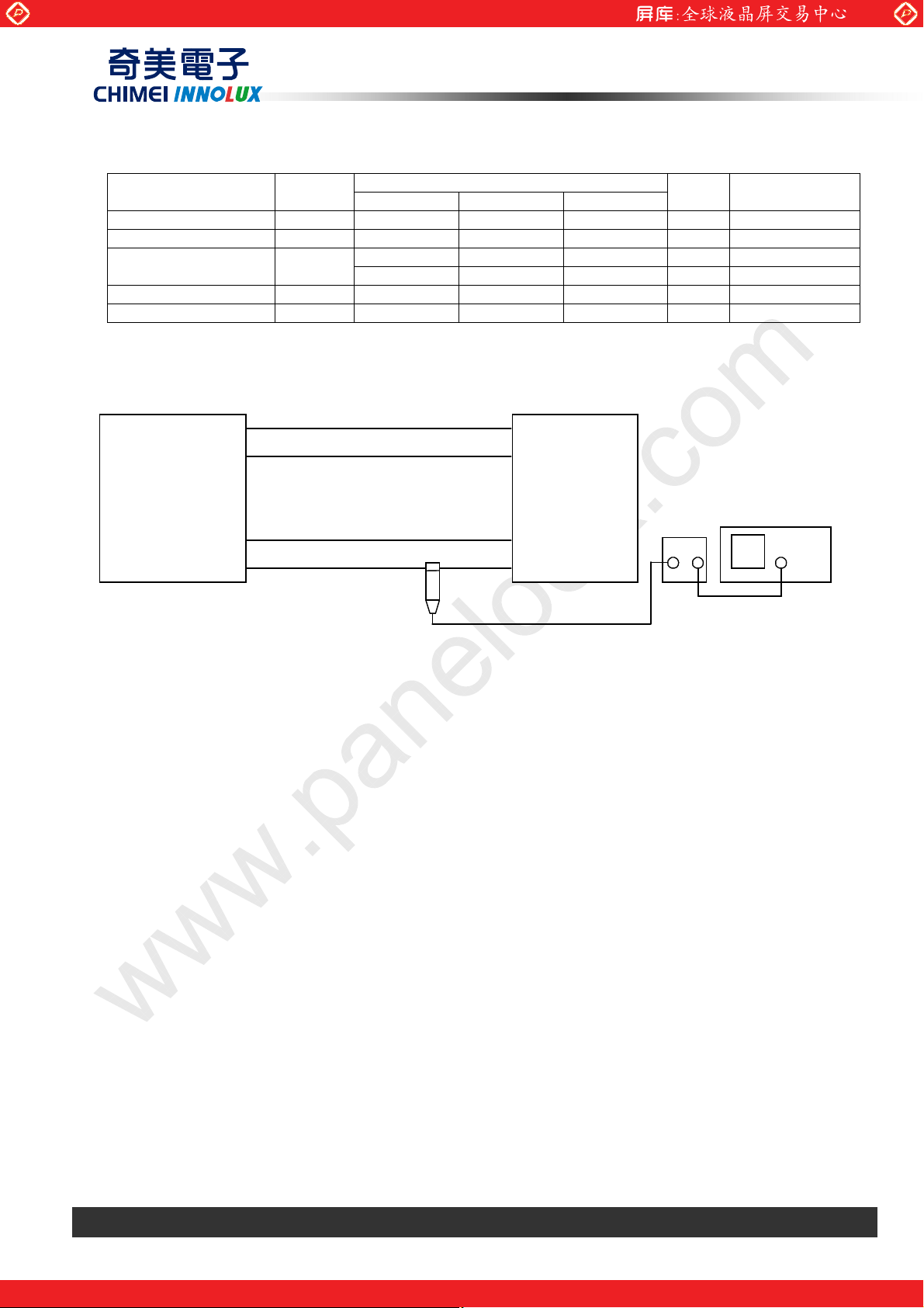
Note (5) Measurement Setup:
The LCD module should be stabilized at given temperature for 60 minutes to avoid abrupt temperature
change during measuring. In order to stabilize the luminance, the measurement should be executed after
lighting Backlight for 60 minutes in a windless room.
LCD Module
LCD Panel
USB2000
CS-1000T
Center of the Screen
500 mm
Light Shield Room
(Ambient Luminance < 2 lux)
Version 2.1 17th, Feb., 2011
The copyright belongs to CHIMEI InnoLux. Any unauthorized use is prohibited.
One step solution for LCD / PDP / OLED panel application: Datasheet, inventory and accessory!
22 / 29
www.panelook.com
Page 23

Global LCD Panel Exchange Center
Note (6) Definition of White Variation (δW):
Measure the luminance of gray level 1023 at 81 points
L
δW =
L
Where:
L
bright
L
dark
Measuring points are shown in the following Figure.
bright
dark
: the Luminance of the point that is brighter than the other point to be compared
: the Luminance of the point that is darker than the other point to be compared
www.panelook.com
PRODUCT SPECIFICATION
Version 2.1 17th, Feb., 2011
The copyright belongs to CHIMEI InnoLux. Any unauthorized use is prohibited.
One step solution for LCD / PDP / OLED panel application: Datasheet, inventory and accessory!
23 / 29
www.panelook.com
Page 24

Global LCD Panel Exchange Center
8. PACKAGING
8.1 PACKING SPECIFICATIONS
(1) 4 LCD modules / 1 Box
(2) Box dimensions: 775(L) X 320(W) X 550(H) mm
(3) Weight: approximately 21.19Kg (4 modules per box)
8.2 PACKING METHOD
(1) Carton Packing should have no failure in the following reliability test items.
Test Item Test Conditions Note
ISTA STANDARD
Random, Frequency Range: 1 – 200 Hz
Vibration
Dropping Test 1 Angle, 3 Edge, 6 Face, 45.7cm Non Operation
Top & Bottom: 30 minutes (+Z), 10 min (-Z),
Right & Left: 10 minutes (X)
Back & Forth 10 minutes (Y)
www.panelook.com
PRODUCT SPECIFICATION
Non Operation
Figure. 8-1 Packing
Version 2.1 17th, Feb., 2011
The copyright belongs to CHIMEI InnoLux. Any unauthorized use is prohibited.
One step solution for LCD / PDP / OLED panel application: Datasheet, inventory and accessory!
24 / 29
www.panelook.com
Page 25

Global LCD Panel Exchange Center
For ocean shipping
www.panelook.com
PRODUCT SPECIFICATION
For air transport
Figure. 8-2 Packing
Figure. 8-3 Packing
Version 2.1 17th, Feb., 2011
The copyright belongs to CHIMEI InnoLux. Any unauthorized use is prohibited.
One step solution for LCD / PDP / OLED panel application: Datasheet, inventory and accessory!
25 / 29
www.panelook.com
Page 26

Global LCD Panel Exchange Center
9. DEFINITION OF LABELS
9.1 MODULE LABEL
The barcode nameplate is pasted on each module as illustration, and its definitions are as following explanation.
www.panelook.com
PRODUCT SPECIFICATION
R300M1 -L01 Rev. XX
CHI MEI
OPTOELECTRONICS
(a) Model Name: R300M1-L01
(b) Revision: Rev. XX, for example: A0, A1… B1, B2… or C1, C2…etc.
(c) Serial ID: X X
X X X X X Y M D L N N N N
X X X X X X X Y M D L N N N N
MADE IN
Serial
Product Line
Year, Month, Date
CMO Internal Use
E207943
MADE IN TAIWAN
Code Meaning Description
XX CMO internal use XX Revision Cover all the change
X CMO internal use -
YMD
L Product line # Line 1=1, Line 2=2, Line 3=3, …
NNNN Serial number Manufacturing sequence of product
CMO Internal Use
Revision
CMO Internal Use
Year, month, day Year: 2001=1, 2002=2, 2003=3, 2004=4…
Month: 1~12=1, 2, 3, ~, 9, A, B, C
Day: 1~31=1, 2, 3, ~, 9, A, B, C, ~, W, X, Y, exclude I, O, and U.
Version 2.1 17th, Feb., 2011
The copyright belongs to CHIMEI InnoLux. Any unauthorized use is prohibited.
One step solution for LCD / PDP / OLED panel application: Datasheet, inventory and accessory!
26 / 29
www.panelook.com
Page 27

Global LCD Panel Exchange Center
10. PRECAUTIONS
10.1 ASSEMBLY AND HANDLING PRECAUTIONS
(1) Do not apply rough force such as bending or twisting to the module during assembly.
(2) To assemble or install module into user’s system can be only in clean working areas. The dust and oil
may cause electrical short or worsen the polarizer.
(3) It’s not permitted to have pressure or impulse on the module because the LCD panel and Backlight will
be damaged.
(4) Always follow the correct power sequence when LCD module is connecting and operating. This can
prevent damage to the CMOS LSI chips during latch-up.
(5) Do not pull the I/F connector in or out while the module is operating.
(6) Do not disassemble the module.
www.panelook.com
PRODUCT SPECIFICATION
(7) Use a soft dry cloth without chemicals for cleaning, because the surface of polarizer is very soft and
easily scratched.
(8) It is dangerous that moisture come into or contacted the LCD module, because moisture may damage
LCD module when it is operating.
(9) High temperature or humidity may reduce the performance of module. Please store LCD module within
the specified storage conditions.
(10)When ambient temperature is lower than 10ºC may reduce the display quality. For example, the
response time will become slowly, and the starting voltage of CCFL will be higher than room temperature.
10.2 SAFETY PRECAUTIONS
(1) The startup voltage of Backlight is approximately 1000 Volts. It may cause electrical shock while
assembling with inverter. Do not disassemble the module or insert anything into the Backlight unit.
(2) If the liquid crystal material leaks from the panel, it should be kept away from the eyes or mouth. In case
of contact with hands, skin or clothes, it has to be washed away thoroughly with soap.
(3) After the module’s end of life, it is not harmful in case of normal operation and storage.
Version 2.1 17th, Feb., 2011
The copyright belongs to CHIMEI InnoLux. Any unauthorized use is prohibited.
One step solution for LCD / PDP / OLED panel application: Datasheet, inventory and accessory!
27 / 29
www.panelook.com
Page 28

Global LCD Panel Exchange Center
www.panelook.com
One step solution for LCD / PDP / OLED panel application: Datasheet, inventory and accessory!
www.panelook.com
Page 29

Global LCD Panel Exchange Center
www.panelook.com
One step solution for LCD / PDP / OLED panel application: Datasheet, inventory and accessory!
www.panelook.com
 Loading...