

Page 1
Global LCD Panel Exchange Center
A
ಖᙕ
ՠ܂
ᐉு
ߡۥ
ދป
Issued Date: Apr. 11, 2007
www.panelook.com
Model No.: R181E1-L01
Approval
TFT LCD Approval Specification
MODEL NO.: R181E1-L01
(IDT ITSX88E)
Customer:
pproved by:
Note:
2007-06-06
15:40:49 CST
Approve by
Dept. Mgr.(QA
RA)
tomy_chen(ຫةԫ
/52720/54140/43150)
Department
Manager(QA RA)
Accept
2007-06-06
13:29:11 CST
2007-05-25
16:05:51 CST
2007-05-21
18:21:24 CST
One step solution for LCD / PDP / OLED panel application: Datasheet, inventory and accessory!
Approve by
Director
Approve by
Director
Review by
Director
wy_li(ޕޫ/44701)
cc_chen(ຫګ/56350/54951)
kf_huang(႓഼
/56620/54380/14906/25075)
1 / 40
Director Accept
Director Accept
Director Accept
Version 2.1
www.panelook.com
Page 2
Global LCD Panel Exchange Center
Issued Date: Apr. 11, 2007
www.panelook.com
Model No.: R181E1-L01
Approval
REVISION HISTORY
Version Date Section Description
Ver 2.0
Ver 2.1
Nov. 29, 06’
Apr. 11, 07’
All
2.1
4.0
Index to IDT OEM I-88E-05
Index to IDT OEM I-88E-06
Contrast spec update(Reference to IDTech 2004 3/31 EC notice)
Contrast spec update(Reference to IDTech 2004 3/31 EC notice)
2 / 40
One step solution for LCD / PDP / OLED panel application: Datasheet, inventory and accessory!
Version 2.1
www.panelook.com
Page 3

Global LCD Panel Exchange Center
Engineering Specification
www.panelook.com
Engineering Specification
Type 18.1 SXGA Monochrome TFT/LCD Module
Model Name: ITSX88E
Document Control Number: OEM I-88E-06
(C) Copyright International Display Technology 2002 All Rights reserved
April 11,2007 OEM I-88E-06
One step solution for LCD / PDP / OLED panel application: Datasheet, inventory and accessory!
3/40
www.panelook.com
Page 4
Global LCD Panel Exchange Center
Engineering Specification
i Contents
i Contents
ii Record of Revision
1.0 Handling Precautions
2.0 General Description
2.1 Characteristics
2.2 Functional Block Diagram
3.0 Absolute Maximum Ratings
4.0 Optical Characteristics
4.1 Luminance Uniformity
4.2 Image Retention
5.0 Signal Interface
5.1 Connectors
5.2 Interface Signal Connector
5.3 Interface Signal Description
5.4 Interface Signal Electrical Characteristics
5.5 Backlight Connector Signal Description
5.6 Backlight Input Signal Electrical Characteristics
6.0 Pixel format image
7.0 Interface Timings
7.1 Timing Characteristics
7.2 Timing Definition
8.0 Power Consumption
9.0 Power ON/OFF Sequence
10.0 Mechanical Characteristics
11.0 National Test Lab Requirement
12.0 Backlight Life
13.0 Packaging Specification
14.0 Label
15.0 Application Note
www.panelook.com
(C) Copyright International Display Technology 2002 All Rights reserved
April 11,2007 OEM I-88E-06
One step solution for LCD / PDP / OLED panel application: Datasheet, inventory and accessory!
4/40
www.panelook.com
Page 5
Global LCD Panel Exchange Center
Engineering Specification
ii Record of Revision
Date Document
Revision
June 13,2001 OEM I-88E-01 All First Edition for customer.
www.panelook.com
Page Summary
Based on Internal Spec. as of June 1,2001
October 23,2001
January 28,2002 OEM I-88E-03 5,8 To update White Luminance.
February 25,2002
OEM I-88E-02
5,8
5
7
8
19
21
24,25
27,28
OEM I-88E-04
4
5
5,8
Update by establishment of the New Company as "International Display
Technology".
Based on Internal Spec. EC H30912 as of October 22,2001.
To update White Luminance.
To update Weight, Optical Rise Time + Fall Time and Power
Consumption.
To update value of Shock Test Criteria.
To update Viewing Angle, Response Time and White Balance.
To update the Lamp Current versus Luminance Curve.
To add Note for Timing Characteristics.
To update Power Consupmtion.
To update Reference Drawings.
Based on Internal Spec. EC H30923.
To add one of item for Handling Precautions.
To update Power Consupmtion.
To update Contrast Ratio.
27
To add Note for Mechanical Characteristics.
(C) Copyright International Display Technology 2002 All Rights reserved
April 11,2007 OEM I-88E-06
5/40
One step solution for LCD / PDP / OLED panel application: Datasheet, inventory and accessory!
www.panelook.com
Page 6
Global LCD Panel Exchange Center
Engineering Specification
www.panelook.com
February 15,2007 OEM I-88E-05
April 11,2007 OEM I-88E-06
13
14
15
35
36,37
38,39
40
8
11
4.0 Optical Characteristics
Optical equipment change.
4.2 Image Retention
Update Image Retention spec
5.1 Connectors
Change IF connector type to RoHs.
Change Inverter connector type to RoHs.
12.0 Backlight Life spec add.
13.0 Packaging Specification add.
14.0 Label spec add.
15.0 Application Note add.
2.1 Characteristics
Contrast Ratio update (IDT ECN at 2004 3/31)
(Typ 550 Æ600,min 300Æ500)
4.0 Optical Characteristics (IDT ECN at 2004 3/31)
Contrast Ratio update
(Typ 550 Æ600,min 300Æ500)
(C) Copyright International Display Technology 2002 All Rights reserved
April 11,2007 OEM I-88E-06
One step solution for LCD / PDP / OLED panel application: Datasheet, inventory and accessory!
6/40
www.panelook.com
Page 7
Global LCD Panel Exchange Center
Engineering Specification
1.0 Handling Precautions
• Damage to the panel or the panel electronics may result from any deviation from the recommended
power on/off sequencing. The panel should not be hot plugged. Refer to the Power On/Off Sequence
section in this Specification.
• Handle the panel with care. The LCD panel and CCFL (Cold Cathode Fluorescent Lamp)s are made of
glass and may crack or break if dropped or subjected to excessive force.
• The CCFLs contain a small amount of Mercury so should not be disposed of to landfill. Dispose of as
required by local ordinances or regulations.
• The LCD module contains small amounts of material having no flammability grade. The exemption
conditions of the flammability requirements (4.7.3.4, IEC60950 3rd.Ed. or UL60950 3rd.Ed.) should be
applied.
• The panel may be damaged by the application of twisting or bending forces to the module
assembly.Care should be taken in the design of the monitor housing and the assembly procedure to
prevent stress damage to the panel especially the lamp cable and the lamp connector..
• Use standard earthing/grounding procedures to prevent damage to the CMOS LSI while handling the
module.
• Use earthing/grounding procedures, an ionic shower, or similar to prevent static damage while
removing the protective front sheet.
• The front polarizer can be easily damaged. Take care not to scratch the front surface with any hard or
abrasive material. Dust, finger marks, grease etc. can be removed with a soft damp cloth (a small
amount of mild detergent can be used on the damp cloth). Do not apply water or detergent directly to
the front surface as this may cause staining or damage the electronic components.
• Never use any solvent on the front polarizer or module as this may cause permanent damage.
• Do not open or modify the module assembly.
• Continuous operation of the panel with the same screen content may result in some image sticking.
Over 10 hours operation with the same content is not recommended.
• Wipe off water drop immediately. Long contact with water may cause discoloration or spots.
• When the panel surface is soiled, wipe it with absorbent cotton or other soft cloth.
• Please do not use middle 3(three) screw holes on the upper(long) side and middle 3(three) screw holes
on the lower(long) side for panel fixing. These screw holes are for manufacturing purpose only.
The information contained herein is presented only as a guide for the applications of our
products. No responsibility is assumed by International Display Technology for any
infringements of patents or other right of the third partied which may result from its use. No
license is granted by implication or otherwise under any patent or patent rights of
International Display Technology or others.
(C) Copyright International Display Technology 2002 All Rights reserved
April 11,2007 OEM I-88E-06
www.panelook.com
7/40
One step solution for LCD / PDP / OLED panel application: Datasheet, inventory and accessory!
www.panelook.com
Page 8
Global LCD Panel Exchange Center
Engineering Specification
2.0 General Description
This specification applies to the Type 18.1 Monochrome TFT/LCD Module 'ITSX88E'.
This module is designed for a LCD monitor style display unit.This module includes inverter card.
The screen format and electrical interface are intended to support the VESA SXGA (1280(H) x 1024(V)at
60Hz) screen.
Supported gray scale is 8-bit per 1(one) sub-pixel.
All input signals are LVDS(Low Voltage Differential Signaling) interface compatible.
This model meet RoHs requirements.
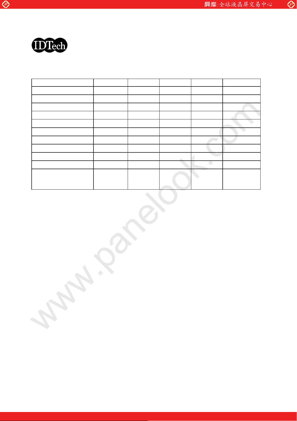
2.1 Characteristics
The following items are characteristics summary on the table under 25 degree C condition:
CHARACTERISTICS ITEMS SPECIFICATIONS
Screen Diagonal [mm] 460
www.panelook.com
Pixels H x V 1280(x3) x 1024
Active Area [mm] 359.0(H) x 287.2(V)
Pixel Pitch [mm] 0.2805(per one triad) x 0.2805
Pixel Arrangement Sub-pixel Vertical Stripe
Weight [grams] 2,900 typ.
Physical Size [mm] 389.0(W) typ. x 317.2(H) typ. x 35.0 (D) max.
Display Mode Normally Black
Display Surface Treatment Anti-Glare
Supported Grayscale 8-bit per 1(one) sub-pixel
White Luminance [cd/m2] 700 Typ.
Contrast Ratio 600 : 1 Typ.
Optical Rise Time/Fall Time [msec] Rise Time + Fall Time : 40 Typ (total)
Input Voltage [V] +12 +/- 5%
Power Consumption [W] 38.8 typ., 46.6 max.
Electrical Interface
Temperature Range [degree C]
Operating
Storage (Shipping)
LVDS Dual
(Even/Odd A/B/C Data(8bit), 3sync signals, Clock)
0 to +50
-20 to +60
(C) Copyright International Display Technology 2002 All Rights reserved
April 11,2007 OEM I-88E-06
8/40
One step solution for LCD / PDP / OLED panel application: Datasheet, inventory and accessory!
www.panelook.com
Page 9
Global LCD Panel Exchange Center
A
Engineering Specification
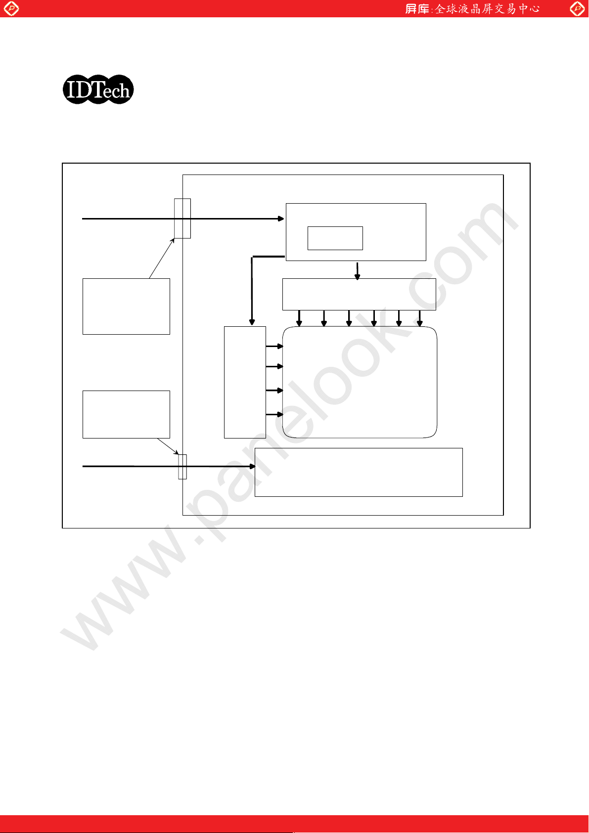
2.2 Functional Block Diagram
The following diagram shows the functional block of this Type 18.1 Monochrome TFT/LCD Module.
www.panelook.com
LCD module
+12V
LVDS Signals
SELLVDS
Connector
HIROSE
DF14-30P-1.25H(59)
Mating
DF14-30S-1.25C
Connector
JST S8B-PH-SM3
Mating
JST PHR-8
+12V
VDIM
BLON
Y-card
Interface card
Gatearray
Backlight unit
Inverter card
X-card
TFT/LCD
rray/Cell
1280x1024
(C) Copyright International Display Technology 2002 All Rights reserved
April 11,2007 OEM I-88E-06
One step solution for LCD / PDP / OLED panel application: Datasheet, inventory and accessory!
9/40
www.panelook.com
Page 10
Global LCD Panel Exchange Center
y
Engineering Specification
3.0 Absolute Maximum Ratings
Absolute maximum ratings of the module is as follows:
www.panelook.com
Item S
Logic/LCD Drive Voltage Vin -0.3 +13.2 V
Backlight Voltage VBL -0.3 +13.2 V
Select LVDS data order SELLVDS -0.3 3.3 V
Brightness control VDIM -0.3 5.3 V
Backlight on signal BLON -0.3 +5.3 V
Operating Temperature TOP 0 +50 deg.C
Operating Humidity HOP 8 80 %RH
Storage Temperature TST -20 +60 deg.C
Storage Humidity HST 5 95 %RH
Vibration 1.5 G Hz
Shock 50 11 G ms
Note 1: Maximum Wet-Bulb should be 39 degree C and No condensation.
Note 2: Vibration Specification
- Sign Vibration:10-200-10Hz, 1.5G, 30 min, X, Y,Z Axis, Each One Time.
Shock Specification
- Half sine wave:50G 11msec. -X+/-, -Y+/-, -Z+/- (Total 6 directions), Each one time Shock.
mbol Min Max Unit Conditions
(Note 1)
(Note 1)
(Note 1)
(Note 1)
(Note 2)
(Note 2)
Half sine
wave
(C) Copyright International Display Technology 2002 All Rights reserved
April 11,2007 OEM I-88E-06
One step solution for LCD / PDP / OLED panel application: Datasheet, inventory and accessory!
10/40
www.panelook.com
Page 11
Global LCD Panel Exchange Center
Engineering Specification
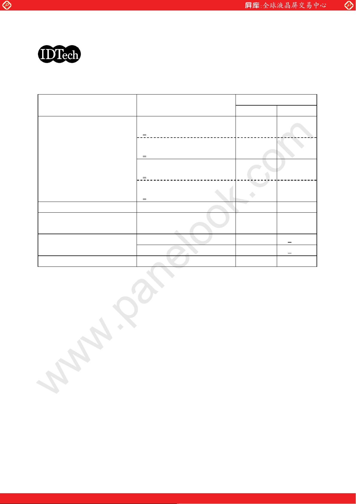
4.0 Optical Characteristics
The optical characteristics are measured under stable conditions as follows under 25 degree C condition:
Item Conditions Specification
Typ. Note
www.panelook.com
Viewing Angle
(Degrees)
K:Contrast Ratio Vertical (Upper)
Horizontal (Right)
Vertical (Upper)
Contrast ratio 600 500 Min.
Response Time (ms)
White Balance White x 0.299 +0.030
White y 0.305 +0.030
Maximum White Luminance (cd/m2) VDIM=0V 700 610 Min.
Measure center of the screen.
Horizontal (Right)
K>
15 (Left)
K>
15 (Lower)
K>
10 (Left)
K>
10 (Lower)
Rising (10%->90%)
+
Falling (90%->10%)
85
85
85
85
-
-
-
-
40 -
-
-
-
-
85 Min.
85 Min.
85 Min.
85 Min.
(C) Copyright International Display Technology 2002 All Rights reserved
April 11,2007 OEM I-88E-06
One step solution for LCD / PDP / OLED panel application: Datasheet, inventory and accessory!
11/40
www.panelook.com
Page 12
Global LCD Panel Exchange Center
Engineering Specification
www.panelook.com
The following is the note for the Optical Characteristics:
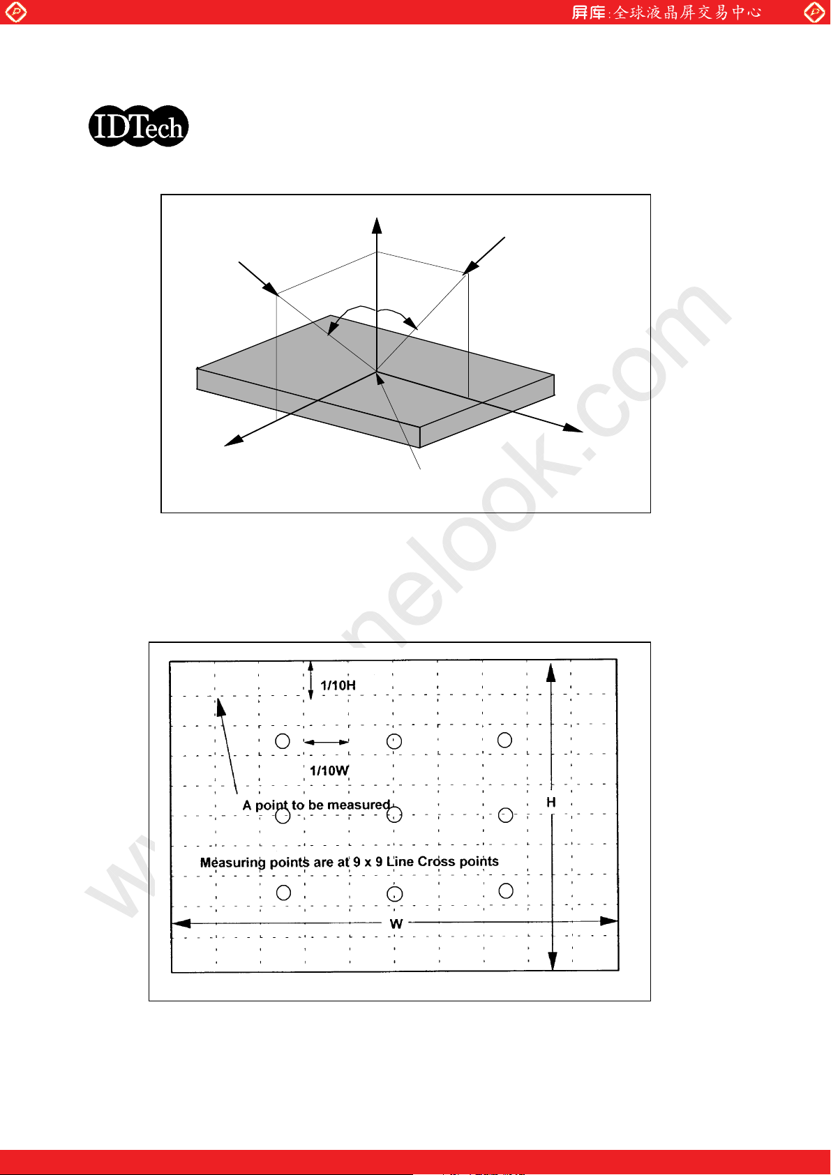
Z
Viewing or Measuring
Direction
LEFT
LOW ER
X
CENTER OF LCD
(X=0,Y=0,Z=0)
Viewing or Measuring
Direction
+h-v
UPPER
RIGHT
Y
There is the Uniformity Measurement below:
'Lbright' represents the Luminance of the point that is brighter than the other point to be compared.
'Ldark' represents the Luminance of the point that is darker than the other point to be compared.
Measuring points are shown in the following Fig. 9 circles are defined for 9 points.
(C) Copyright International Display Technology 2002 All Rights reserved
April 11,2007 OEM I-88E-06
One step solution for LCD / PDP / OLED panel application: Datasheet, inventory and accessory!
12/40
www.panelook.com
Page 13

Global LCD Panel Exchange Center
Engineering Specification
Chromaticity and White Balance are defined as the C.I.E. 1931 x,y coordinates at the center of LCD.
The Standard Equipment are as shown below table.
Item Standard Equipment
Viewing Angle BM5A by Topcon Optical
Contrast USB 2000 Ocean Optics
Response Time 6030 Lecory
White Luminance USB 2000 Ocean Optics
Luminance Uniformity USB 2000 Ocean Optics
Chromaticity CS1000T by Konica Minolta
White Balance USB 2000 Ocean Optics
The measurement is to be done after 120 minutes of Power-on of BackLight.
Unless otherwise specified, the ambient conditions are as following.
Ambient Temperature : 25 + 2 ( degreeC )
Ambient Humidity : 25 - 85 ( % )
Atmospheric Pressure : 86.0 - 104.0 ( kPa )
4.1 Luminance Uniformity
When the backlight is on with all pels in the selected state (white), the luminance uniformity is defined as follows;
Where:
: The luminance of the brightness part of the area
L
bright
: The luminance of the darkest part of the area
L
dark
1. Adjacent Area
L
Luminance Uniformity = > 0.90
L
over a circular area of 10mm diameter placed anywhere on the screen.
2. Screen Total
L
Luminance Uniformity = > 0.70
L
over the entire screen.
dark
bright
dark
bright
www.panelook.com
3. Screen Total (9 points measurement)
L
Luminance Uniformity = >
L
dark
bright
0.80
over the entire screen.
(C) Copyright International Display Technology 2002 All Rights reserved
April 11,2007 OEM I-88E-06
One step solution for LCD / PDP / OLED panel application: Datasheet, inventory and accessory!
13/40
www.panelook.com
Page 14

Global LCD Panel Exchange Center
Engineering Specification
4.2 Image Retention
The panel spec of image sticking / retention is as follows.
Test method: The L0/L255 Window pattern below is displayed for the display time
Then, change the pattern to L128 All gray pattern and count the time
until the retention/sticking image disappears.
Display Time 5sec 60sec
www.panelook.com
Time until disappearing
Definition of disappearing time: The time when the brightness will reach to 0.89% difference from background
level (L128).
| L logo − L128 |
x 100 <
L128
0.89%
5sec 15sec
1
2
1
2
1
1
(C) Copyright International Display Technology 2002 All Rights reserved
April 11,2007 OEM I-88E-06
One step solution for LCD / PDP / OLED panel application: Datasheet, inventory and accessory!
L128
14/40
www.panelook.com
Page 15

Global LCD Panel Exchange Center
Engineering Specification
www.panelook.com
5.0 Signal Interface
5.1 Connectors
Physical interface is described as for the connector on module.
These connectors are capable of accommodating the following signals and will be following components.
Connector Name / Designation Signal Connector
Manufacturer HIROSE
Type / Part Number DF14-30P-1.25H(56)
Mating Type / Part Number DF14-30S-1.25C
Contact / Part Number DF14-2628SCFA
Connector Name / Designation For Backlight Connector on Inverter card
Manufacturer JST
Type / Part Number S8B-PH-SM3-TB(D)(LF) or
S8B-PH-SM4-TB(LF)(SN)
Mating Type / Part Number PHR-8
(C) Copyright International Display Technology 2002 All Rights reserved
April 11,2007 OEM I-88E-06
One step solution for LCD / PDP / OLED panel application: Datasheet, inventory and accessory!
15/40
www.panelook.com
Page 16

Global LCD Panel Exchange Center
Engineering Specification
5.2 Interface Signal Connector
Pin # Signal Name Pin # Signal Name
30 Vin(+12V) 29 Vin(+12V)
28 Vin(+12V) 27 VinRTN(GND)
26 VinRTN(GND) 25 VinRTN(GND)
www.panelook.com
24 SELLVDS 23
22 DGND 21 RxOIN3+
20 RxOIN3- 19 RxOCLKIN+
18 RxOCLKIN- 17 RxOIN2+
16 RxOIN2- 15 RxOIN1+
14 RxOIN1- 13 RxOIN0+
12 RxOIN0- 11 RxEIN3+
10 RxEIN3- 9 RxECLKIN+
8 RxECLKIN- 7 RxEIN2+
6 RxEIN2- 5 RxEIN1+
4 RxEIN1- 3 RxEIN0+
2 RxEIN0- 1 LVDSGND
Note1: Please set this line open.
(RESERVED) Note1
(C) Copyright International Display Technology 2002 All Rights reserved
April 11,2007 OEM I-88E-06
One step solution for LCD / PDP / OLED panel application: Datasheet, inventory and accessory!
16/40
www.panelook.com
Page 17

Global LCD Panel Exchange Center
Engineering Specification
5.3 Interface Signal Description
The module uses a pair of LVDS receiver SN75LVDS82(Texas Instruments) or compatible. LVDS is a differential
signal technology for LCD interface and high speed data transfer device. Transmitter shall be
SN75LVDS83(negative edge sampling) or compatible.
The first LVDS port (RxExxx) transmits even pixels while the second LVDS port (RxOxxx) transmits odd pixels.
Pin numberings have been changed from previous models of ITSX94, ITSX94N, ITSX94N1, and ITSX96R, due to
signal connector type change. Physical order of singals are not changed.
Please refer to the chart below for pin #1.
LCD Drive Connector No.1 Pin location
www.panelook.com
Pin No.1
Module Back side view
(C) Copyright International Display Technology 2002 All Rights reserved
April 11,2007 OEM I-88E-06
Signal Connector
17/40
One step solution for LCD / PDP / OLED panel application: Datasheet, inventory and accessory!
www.panelook.com
Page 18

Global LCD Panel Exchange Center
Engineering Specification
PIN # SIGNAL NAME Description
30 Vin +12.0V Power Supply
29 Vin +12.0V Power Supply
28 Vin +12.0V Power Supply
27 VinRTN Ground for Vin line
26 VinRTN Ground for Vin line
25 VinRTN Ground for Vin line
24 SELLVDS Select LVDS data order. See the following figure.
23 (RESERVED) This pin should be left open.
22 DGND Signal Ground
www.panelook.com
21 RxOIN3+ Positive LVDS differential data input (Odd data)
20 RxOIN3- Negative LVDS differential data input (Odd data)
19 RxOCLKIN+ Positive LVDS differential clock input (Odd Clock)
18 RxOCLKIN- Negative LVDS differential clock input (Odd Clock)
17 RxOIN2+ Positive LVDS differential data input (Odd data)
16 RxOIN2- Negative LVDS differential data input (Odd data)
15 RxOIN1+ Positive LVDS differential data input (Odd data)
14 RxOIN1- Negative LVDS differential data input (Odd data)
13 RxOIN0+ Positive LVDS differential data input (Odd data)
12 RxOIN0- Negative LVDS differential data input (Odd data)
11 RxEIN3+ Positive LVDS differential data input (Even data)
10 RxEIN3- Negative LVDS differential data input (Even data)
9 RxECLKIN+ Positive LVDS differential clock input (Even Clock)
8 RxECLKIN- Negative LVDS differential clock input (Even Clock)
7 RxEIN2+ Positive LVDS differential data input (Even data,H-Sync,V-Sync,DSPTMG)
6 RxEIN2- Negative LVDS differential data input (Even data,H-Sync,V-Sync,DSPTMG)
5 RxEIN1+ Positive LVDS differential data input (Even data)
4 RxEIN1- Negative LVDS differential data input (Even data)
3 RxEIN0+ Positive LVDS differential data input (Even data)
2 RxEIN0- Negative LVDS differential data input (Even data)
1 DGND Signal Ground
Note: Input signals of odd and even clock shall be the same timing.
The interface card has a 100ohm resistor between positive and negative lines of each LVDS signal input on the
internal circuit.
(C) Copyright International Display Technology 2002 All Rights reserved
April 11,2007 OEM I-88E-06
One step solution for LCD / PDP / OLED panel application: Datasheet, inventory and accessory!
18/40
www.panelook.com
Page 19

Global LCD Panel Exchange Center
Engineering Specification
(SELLVDS=Low)
RxECLKIN+
RxECLKIN-
www.panelook.com
1 cycle
RxEIN0+
RxEIN0-
RxEIN1+
RxEIN1-
RxEIN2+
RxEIN2-
RxEIN3+
RxEIN3-
RxOCLKIN+
RxOCLKIN-
RxOIN0+
RxOIN0-
RxOIN1+
RxOIN1-
EA1
EB2
EC3
EA7
OA1
OB2
EA0
EB1
EC2
EA6
OA0
OB1
EB0
EC1
DSP
NA
OB0
OC1
EA5
EC0
V-S
EC7
OA5
OC0
EA4
EB5
H-S
EC6
OA4
OB5
EA3
EB4
EC5
EB7
1 cycle
OA3
OB4
EA2
EB3
EC4
EB6
OA2
OB3
EA1
EB2
EC3
EA7
OA1
OB2
EA0
EB1
EC2
EA6
OA0
OB1
EB0
EC1
DSP
NA
OB0
OC1
RxOIN2+
RxOIN2-
RxOIN3+
RxOIN3-
OC3
OA7
OC2
OA6
NA
NA
NA
OC7
NA
OC6
OC5
OB7
OC4
OB6
OC3
OA7
OC2
OA6
NA
NA
Note: A/B/C data 7:MSB, A/B/C data 0:LSB
(C) Copyright International Display Technology 2002 All Rights reserved
April 11,2007 OEM I-88E-06
19/40
One step solution for LCD / PDP / OLED panel application: Datasheet, inventory and accessory!
www.panelook.com
Page 20

Global LCD Panel Exchange Center
Engineering Specification
(SELLVDS=High)
RxECLKIN+
RxECLKIN-
www.panelook.com
1 cycle
RxEIN0+
RxEIN0-
RxEIN1+
RxEIN1-
RxEIN2+
RxEIN2-
RxEIN3+
RxEIN3-
RxOCLKIN+
RxOCLKIN-
RxOIN0+
RxOIN0-
RxOIN1+
RxOIN1-
EA3
EB4
EC5
EA1
OA3
OB4
EA2
EB3
EC4
EA0
OA2
OB3
EB2
EC3
DSP
NA
OB2
OC3
EA7
EC2
V-S
EC1
OA7
OC2
EA6
EB7
H-S
EC0
OA6
OB7
EA5
EB6
EC7
EB1
1 cycle
OA5
OB6
EA4
EB5
EC6
EB0
OA4
OB5
EA3
EB4
EC5
EA1
OA3
OB4
EA2
EB3
EC4
EA0
OA2
OB3
EB2
EC3
DSP
NA
OB2
OC3
RxOIN2+
RxOIN2-
RxOIN3+
RxOIN3-
OC5
OA1
OC4
OA0
NA
NA
NA
OC1
NA
OC0
OC7
OB1
OC6
OB0
OC5
OA1
OC4
OA0
NA
NA
Note: A/B/C data 7:MSB, A/B/C data 0:LSB
(C) Copyright International Display Technology 2002 All Rights reserved
April 11,2007 OEM I-88E-06
20/40
One step solution for LCD / PDP / OLED panel application: Datasheet, inventory and accessory!
www.panelook.com
Page 21

Global LCD Panel Exchange Center
Engineering Specification
www.panelook.com
The following is LVDS Signal description.
LVDS DATA NAME Description
DSP
V-S
H-S
TI LVDS X'mitter
(SN75LVDS83)
Signal name
D0
D1
D2
D3
D4
D5
D6
D7
D8
D9
D10
D11
D12
D13
D14
D15
D16
D17
D18
D19
D20
D21
D22
D23
D24
D25
D26
D27
Note:
SELLVDS: Pin#7 of Signal connector
A0: LSB, A7: MSB
Display Timing
Vertical Sync
Horizontal Sync
ITSX88E LVDS Signal
(SELLVDS=Low)
A0
A1
A2
A3
A4
A7
A5
B0
B1
B2
B6
B7
B3
B4
B5
C0
C6
C7
C1
C2
C3
C4
C5
NA
H Sync
V Sync
Disp Timing
A6
When the signal is high, the pixel data shall be valid to be
displayed.
Both Positive and negative polarity are acceptable.
Both Positive and negative polarity are acceptable.
ITSX88E LVDS Signal
(SELLVDS=High)
A2
A3
A4
A5
A6
A1
A7
B2
B3
B4
B0
B1
B5
B6
B7
C2
C0
C1
C3
C4
C5
C6
C7
NA
H Sync
V Sync
Disp Timing
A0
5.4 Interface Signal Electrical Characteristics
(C) Copyright International Display Technology 2002 All Rights reserved
April 11,2007 OEM I-88E-06
One step solution for LCD / PDP / OLED panel application: Datasheet, inventory and accessory!
21/40
www.panelook.com
Page 22

Global LCD Panel Exchange Center
Engineering Specification
Input signals shall be low or Hi-Z state when Vin is off.
It is recommended to refer the specifications of SN75LVDS82DGG(Texas Instruments) in detail.
Signal electrical characteristics are as follows;
Parameter Condition Min Max unit
www.panelook.com
Vth
Vtl
LVDS Timing
Differential Input High Voltage
(Vcm=+1.2V)
Differential Input High Voltage
(Vcm=+1.2V)
100 mV
-100 mV
LVDS Macro AC characteristics.
(C) Copyright International Display Technology 2002 All Rights reserved
April 11,2007 OEM I-88E-06
One step solution for LCD / PDP / OLED panel application: Datasheet, inventory and accessory!
22/40
www.panelook.com
Page 23

Global LCD Panel Exchange Center
Engineering Specification
Parameter Symbol Min Typ Max Unit
LVDS Clock Cycle Trxc 17.6 18.5 20 [ns]
LVDS Data Cycle Trxd Trxc/7 [ns]
www.panelook.com
Sample Data Setup Time
(Trxc=Typ.)
Sample Data Hold Time
(Trxc=Typ.)
Data Sample Time Trxs Trxc/14 [ns]
Data Sample Cycle Trxsc Trxc/7 [ns]
Name Description Min Typ Max Unit Note
SELLVDS High voltage 2 3 3.3 V
Low voltage -0.1 0 0.7 V
Current -1 - 1 mA
Trxss 600 [ps]
Trxsh 600 [ps]
5.5 Backlight Connector Signal Description
(C) Copyright International Display Technology 2002 All Rights reserved
April 11,2007 OEM I-88E-06
One step solution for LCD / PDP / OLED panel application: Datasheet, inventory and accessory!
23/40
www.panelook.com
Page 24

Global LCD Panel Exchange Center
Engineering Specification
PIN # SIGNAL NAME Description
1 VBL +12.0V Power Supply for backlight
2 VBL +12.0V Power Supply for backlight
3 VBL +12.0V Power Supply for backlihgt
4 RTN Ground for VBL line, VDIM and BLON
5 RTN Ground for VBL line, VDIM and BLON
6 RTN Ground for VBL line, VDIM and BLON
7 VDIM Brightness control voltage input(0-4V), (0V:brightness MAX, 4V:brightness MIN)
8 BLON backlihgt on/off signal(Hi:backlight ON, Low:backlight OFF) TTL level
5.6 Backlight Input Signal Electrical Characteristics
Name Description Min Typ Max Unit Note
www.panelook.com
BLON High voltage 2.0 5.0 5.25 V
Low voltage -0.1 0 0.8 V
Current -1.0 - 1.0 mA
VDIM Input Voltage Range 0 - 4.0 V
Current -1.0 - 1.0 mA
0V:Brightness Max.
4V:Brightness Min.
(C) Copyright International Display Technology 2002 All Rights reserved
April 11,2007 OEM I-88E-06
One step solution for LCD / PDP / OLED panel application: Datasheet, inventory and accessory!
24/40
www.panelook.com
Page 25

Global LCD Panel Exchange Center
Engineering Specification
The following chart is the Dimming Signal (VDIM) versus Luminance curve for your reference.
ITSX88E Dimming Curve (VDIM vs Lumi.)
120.0%
100.0%
80.0%
www.panelook.com
Luminance(%)
60.0%
40.0%
20.0%
0.0%
0 0.5 1 1.5 2 2.5 3 3.5 4
VDIM(V)
Lumi(%)
.0 Pixel format image
6
(C) Copyright International Display Technology 2002 All Rights reserved
April 11,2007 OEM I-88E-06
One step solution for LCD / PDP / OLED panel application: Datasheet, inventory and accessory!
25/40
www.panelook.com
Page 26

Global LCD Panel Exchange Center
Engineering Specification
Following figure shows the relationship of the input signals and LCD pixel format image. Odd and even pair of
ABC data are sampled at a time.
Even
0 1 1279
www.panelook.com
Odd Even Odd
1278
1st Line
1024th Line
ABC
A
B
A
A
A
C
B
C
B
C
B
A
ABC
C
ABC
C
B
7
.0 Interface Timings
Basically, interface timings described here is not actual input timing of LCD module but output timing of
SN75LVDS82DGG(Texas Instruments) or equivalent.
(C) Copyright International Display Technology 2002 All Rights reserved
April 11,2007 OEM I-88E-06
One step solution for LCD / PDP / OLED panel application: Datasheet, inventory and accessory!
26/40
www.panelook.com
Page 27

Global LCD Panel Exchange Center
p
p
p
p
play
Engineering Specification
7.1 Timing Characteristics
Signal Item Symbol MIN. TYP. MAX. Unit
www.panelook.com
DTCLK Freq. Fdck
DTCLK Cycle Tck 17.6 18.5
+V-Sync Frame Rate 56.25 60.02 61 Hz
+V-Sync Cycle Tv 16.39 16.66 17.78 ms
+V-Sync Cycle Tv 1035 1066
+V-Sync active level Tva 3 3
+V-Sync V-back
+V-Sync V-front
DSPTMG m - lines
+ V-Line 1024
+H-Sync Scan Rate 1/Th
+H-Sync Cycle Th 844 844
+H-Sync ac l Thtive leve a(*1) 4 56
+H-Sync Back
+H-Sync Front
DSPTMG is
+ D
te1: Typic e is refer to V TANDAR
No al valu ESA S D.
Tha+Thb sho s th Tc
(*1): uld be les an 1024 k.
Note2: When there are invalid timing, Display appears black pattern.
chronous Signa a h for u ction
Syn l Defects nd enter Auto Refres LCD Mod le Prote Mode.
orch Tvb 7 38 63 lines
orch
orch Thb(*1) 4 124
orch
Pixels
11/Tv
Tvf 1 1 lines
Thf 4 24 Tck
n - 640 Tck
50
-
54 56.8 MHz
63.98
20
2047
-
-
1023
-
ns
lines
lines
KHz
Tck
Tck
Tck
.2 Timing Definition
7
V
ertical Timing
(C) Copyright International Display Technology 2002 All Rights reserved
April 11,2007 OEM I-88E-06
27/40
One step solution for LCD / PDP / OLED panel application: Datasheet, inventory and accessory!
www.panelook.com
Page 28

Global LCD Panel Exchange Center
Engineering Specification
www.panelook.com
DSPTMG
-VSYNC
+VSYNC
Support mode
1280 x 1024 at 60Hz
(VESA STANDARD)
(H line rate : 15.6 us)
Horizontal Timing
DSPTMG
-HSYNC
T3 T5 T6
T1 Vertical
Blanking
0.656 ms
(42 lines)
T1 T2
T2
Active Field
16.005 ms
(1024
lines)
T9 T11 T12
T7 T8
T4
T3 VSYNC
Front Porch
0.016 ms
(1 line)
T10
T4
Frame Time
16.661 ms
(1066 lines)
T5 VSYNC
Width
0.047 ms
(3 lines)
T6 VSYNC
Back Porch
0.594 ms
(38 lines)
+HSYNC
Support mode T7
1280 x 1024
(VESA STANDARD)
Horizontal
3.778 us
(408 dots)
T8
Active Field
11.852 us
(1280 dots)
T9
HSYNC
0.444 us
(48 dots)
T10
H line Time
15.630 us
(1688 dots)
T11
HSYNC
1.037 us
(112 dots)
T12
HSYNC
2.296 us
(248 dots)
(Dotclock : 108.000
(C) Copyright International Display Technology 2002 All Rights reserved
April 11,2007 OEM I-88E-06
28/40
One step solution for LCD / PDP / OLED panel application: Datasheet, inventory and accessory!
www.panelook.com
Page 29

Global LCD Panel Exchange Center
Engineering Specification
Interface Timing Definition
Tva
V-Sync
H-Sync
www.panelook.com
Tv
DSPTMG
H-Sync
Dot clock
DSPTMG
Video(Even)
Video(Odd)
Tck
Tha
Tvb Tvf
01 m-1
Vsync, Hsync and Display Timing
Th
Thd
Thb Thf
0
1
2
3
Video signal, Hsync and Dot clock
n-2
n-1
(C) Copyright International Display Technology 2002 All Rights reserved
April 11,2007 OEM I-88E-06
One step solution for LCD / PDP / OLED panel application: Datasheet, inventory and accessory!
29/40
www.panelook.com
Page 30

Global LCD Panel Exchange Center
Engineering Specification
8.0 Power Consumption
Input power specifications are as follows;
SYMBOL PARAMETER Min Typ Max UNITS CONDITION
Vin
Iin Vin Current 550 mA
Pin(1) Vin Power 4.5 W
Pin(2) 5.2 6.3 W
Logic/LCD Drive
Voltage
www.panelook.com
11.4 12 12.6 V
All White Pattern
Vin=11.4V *1
Typical Load Condition
(Vertical Gray Bar, 256 Scale)
Maximum Load
Condition
(All White)
Vin rp
VBL
PBL
(Note) A used DC power supply for this LCD module should be have a over current protection function to safety.
*1 This value indicates long term average.
Logic/LCD DC
current
Waveform
Allowable
Logic/LCD Drive
Ripple Voltage
Backlight power
voltage
Backlight power
consumption
Refer to the Typical Logic/LCD
Current Waveform shown in the
following Figure. Waveform may
vary in paticular application.
Actual current waveform on user
application must be evaluated and
make sure the ripple current
and/or peak current should be
allowable to user power supply.
500 mVp-p
11.4 12 12.6 V
33.6 40.3 W Brightness = max.
Maximum Load
Condition
(All White)
Typical Logic/LCD Current Waveform
(C) Copyright International Display Technology 2002 All Rights reserved
April 11,2007 OEM I-88E-06
One step solution for LCD / PDP / OLED panel application: Datasheet, inventory and accessory!
30/40
www.panelook.com
Page 31

Global LCD Panel Exchange Center
Engineering Specification
Condition: Maximum Load Condition(All White)
Voltage: 12.0V measured at Interface Connector J1
Interface Cable: AWG28, 30 Conductors, L=500mm from Voltage Source to EUT
www.panelook.com
9.0 Power ON/OFF Sequence
(C) Copyright International Display Technology 2002 All Rights reserved
April 11,2007 OEM I-88E-06
31/40
One step solution for LCD / PDP / OLED panel application: Datasheet, inventory and accessory!
www.panelook.com
Page 32

Global LCD Panel Exchange Center
Engineering Specification
Vin and VBL power and lamp on/off sequence is as follows. Interface signals are also shown in the chart. Signals
from any system shall be Hi-Z state or low level when Vin and VBL are off.
It is recommended that the BLON should be supplied after other signals are stable in order to avoid visible screen
noise when power-on.
www.panelook.com
Vin
0 V
Signals
0 V
VBL
0 V
BLON
0 V
10%
10%
90%
30ms max. and 1ms min.
0 min. 0 min.
10%
90%
30ms max. and 1ms min.
5ms min. 0 min.
1.9V
0.9V
1uS max.
90%
10% 10%
10ms min.
10%
100ms min.
90%
10% 10%
1.9V
0.9V
1uS max.
10.0 Mechanical Characteristics
Note: Please do not use middle 3(three) screw holes on the upper(long) side and middle 3(three) screw holes
(C) Copyright International Display Technology 2002 All Rights reserved
April 11,2007 OEM I-88E-06
32/40
One step solution for LCD / PDP / OLED panel application: Datasheet, inventory and accessory!
www.panelook.com
Page 33

Global LCD Panel Exchange Center
Engineering Specification
on the lower(long) side for panel fixing. These screw holes are for manufacturing purpose only.
www.panelook.com
(C) Copyright International Display Technology 2002 All Rights reserved
April 11,2007 OEM I-88E-06
One step solution for LCD / PDP / OLED panel application: Datasheet, inventory and accessory!
33/40
www.panelook.com
Page 34

Global LCD Panel Exchange Center
Engineering Specification
Engineering Specification
www.panelook.com
(C) Copyright International Display Technology 2002 All Rights reserved
(C) Copyright International Display Technology 2002 All Rights reserved
April 11,2007 OEM I-88E-06
April 11,2007 OEM I-88E-06
One step solution for LCD / PDP / OLED panel application: Datasheet, inventory and accessory!
34/40
34/40
www.panelook.com
Page 35

Global LCD Panel Exchange Center
Engineering Specification
11.0 National Test Lab Requirement
The display module is authorized to Apply the UL Recognized Mark.
Conditions of Acceptability
Conditions of Acceptability - When installed on the end-product, consideration shall be given to the following;
1. This component has been judged on the basis of the required spacings in the Standard for Safety of
Information Technology Equipment, CAN/CSA C22.2 No. 60950-00 *UL60950, Third Edition, which are
based on the IEC 60950, Third Edition, which would cover the component itself if submitted for Listing.
2. The inverter output circuits are Limited Current Circuits.
3. The units are intended to be supplied by SELV.
4. The terminals and connectors are suitable for factory wiring only.
5. A suitable Electrical enclosure shall be provided.
www.panelook.com
12.0 Backlight Life
Backlight Life Time 50,000 Hours (Typ) condition 25 degree C
30,000 Hours (Min)
The assumed Backlight Life will be until the luminance becomes 305 cd/m
2
or more at maximum white luminance.
(C) Copyright International Display Technology 2002 All Rights reserved
April 11,2007 OEM I-88E-06
One step solution for LCD / PDP / OLED panel application: Datasheet, inventory and accessory!
35/40
www.panelook.com
Page 36

Global LCD Panel Exchange Center
Engineering Specification
13.0 Packaging Requirement
The packaging of the LCD meets 75 cm drop test.
The following is the drawing of the package.
www.panelook.com
(C) Copyright International Display Technology 2002 All Rights reserved
April 11,2007 OEM I-88E-06
One step solution for LCD / PDP / OLED panel application: Datasheet, inventory and accessory!
36/40
www.panelook.com
Page 37

Global LCD Panel Exchange Center
Engineering Specification
www.panelook.com
(C) Copyright International Display Technology 2002 All Rights reserved
April 11,2007 OEM I-88E-06
One step solution for LCD / PDP / OLED panel application: Datasheet, inventory and accessory!
37/40
www.panelook.com
Page 38

Global LCD Panel Exchange Center
Engineering Specification
14.0 Label
There are labels on the rear side of the Module.
www.panelook.com
Serial Number Label
BARCODE CHARACTER AREA
(C) Copyright International Display Technology 2002 All Rights reserved
April 11,2007 OEM I-88E-06
One step solution for LCD / PDP / OLED panel application: Datasheet, inventory and accessory!
38/40
www.panelook.com
Page 39

Global LCD Panel Exchange Center
Engineering Specification
Date Label
YY and WW of the Week Code stand for the Year and the Week of the Year of manufacturing of the Module
respectively.
UL Label
www.panelook.com
(C) Copyright International Display Technology 2002 All Rights reserved
April 11,2007 OEM I-88E-06
One step solution for LCD / PDP / OLED panel application: Datasheet, inventory and accessory!
39/40
www.panelook.com
Page 40

Global LCD Panel Exchange Center
Engineering Specification
15.0 Application Note
The table below shows the maximum component temperature Spec.
Component Max. Temp. Spec (degree C)
Gate Array 95
X-Driver IC 85
Transformer (Inverter) 105
Inductor Coil (DC/DC) 100
Polarizer (Cell) 60
www.panelook.com
****** End Of Page ******
(C) Copyright International Display Technology 2002 All Rights reserved
April 11,2007 OEM I-88E-06
One step solution for LCD / PDP / OLED panel application: Datasheet, inventory and accessory!
40/40
www.panelook.com
 Loading...