

Page 1
Global LCD Panel Exchange Center
ಖᙕ
ՠ܂
ᐉு
ߡۥ
ދป
TFT LCD Tentative Specification
MODEL NO.: N156O6-L04
www.panelook.com
Issued Date :Feb, 17, 2009
Model No.: N156O6-L04
Tentative
Customer :
Approved by :
Note :
2009-03-12
10:43:16 CST
PMMD III
Director
annie_hsu(ஊՅ≮
/56522 / 54873)
Director Accept
1 / 28
One step solution for LCD / PDP / OLED panel application: Datasheet, inventory and accessory!
Version 0.0
www.panelook.com
Page 2
Global LCD Panel Exchange Center
www.panelook.com
Issued Date :Feb, 17, 2009
Model No.: N156O6-L04
Tentative
- CONTENTS –
-
REVISION HISTORY ------------------------------------------------------- 3
1. GENERAL DESCRIPTION
1.1 OVERVIEW
1.2 FEATURES
1.3 APPLICATION
1.4 GENERAL SPECIFICATIONS
1.5 MECHANICAL SPECIFICATIONS
------------------------------------------------------- 4
2. ABSOLUTE MAXIMUM RATINGS ------------------------------------------------------- 5
2.1 ABSOLUTE RATINGS OF ENVIRONMENT
2.2 ELECTRICAL ABSOLUTE RATINGS
2.2.1 TFT LCD MODULE
2.2.2 BACKLIGHT UNIT
3. ELECTRICAL CHARACTERISTICS ------------------------------------------------------- 7
3.1 TFT LCD MODULE
3.2 BACKLIGHT UNIT
4. BLOCK DIAGRAM ------------------------------------------------------- 10
4.1 TFT LCD MODULE
5. INPUT TERMINAL PIN ASSIGNMENT ------------------------------------------------------- 10
5.1 TFT LCD MODULE
5.2 BACKLIGHT FPC PIN ASSIGNMENT
5.3 TIMING DIAGRAM OF LVDS INPUT SIGNAL
5.4 COLOR DATA INPUT ASSIGNMENT
5.5 EDID DATA STRUCTURE
6. INTERFACE TIMING ------------------------------------------------------- 14
6.1 INPUT SIGNAL TIMING SPECIFICATIONS
6.2 POWER ON/OFF SEQUENCE
7. OPTICAL CHARACTERISTICS
7.1 TEST CONDITIONS
7.2 OPTICAL SPECIFICATIONS
------------------------------------------------------- 20
8. PRECAUTIONS ------------------------------------------------------- 24
8.1 HANDLING PRECAUTIONS
8.2 STORAGE PRECAUTIONS
8.3 OPERATION PRECAUTIONS
9. PACKING ------------------------------------------------------- 25
9.1 CARTON
9.2 PALLET
10. DEFINITION OF LABELS ------------------------------------------------------- 25
10.1 CMO MODULE LABEL
10.2 CARTON LABEL
2 / 28
One step solution for LCD / PDP / OLED panel application: Datasheet, inventory and accessory!
Version 0.0
www.panelook.com
Page 3
Global LCD Panel Exchange Center
www.panelook.com
Issued Date :Feb, 17, 2009
Model No.: N156O6-L04
Tentative
REVISION HISTORY
Version Date
Ver 0.0 Feb.17, 2009 All All Tentative specification first issued.
Page
(New)
Section Description
3 / 28
One step solution for LCD / PDP / OLED panel application: Datasheet, inventory and accessory!
Version 0.0
www.panelook.com
Page 4
Global LCD Panel Exchange Center
www.panelook.com
Issued Date :Feb, 17, 2009
Model No.: N156O6-L04
Tentative
1. GENERAL DESCRIPTION
1.1 OVERVIEW
N156O6-L04 is a 15.6” ΰ15.547" diagonal)TFT Liquid Crystal Display module with LED Backlight unit
and 40 pins LVDS interface. This module supports 1600 x 900 WXGA+ mode and can display 262,144
colors. The optimum viewing angle is at 6 o’clock direction. The converter module for backlight is built
in.
1.2 FEATURES
- Thing and Light
- WXGA+ (1600x900 pixels) resolution.
- VESA standard LED model.
- 3.3V LVDS (Low Voltage Differential Signaling) interface with 2 pixel/clock
- RoHS compliance
1.3 APPLICATION
- TFT LCD Notebook
1.4 GENERAL SPECIFICATI0NS
Item Specification Unit Note
Active Area 344.16 (H) x 193.59 (V) (15.547” diagonal) mm
Polarizer CF 347.36(H) x 196.59(V) mm
Driver Element a-si TFT active matrix - Pixel Number 1600 x R.G.B. x 900 pixel Pixel Pitch 0.215 (H) x 0.215 (V) mm Pixel Arrangement RGB vertical stripe - Display Colors 262,144 color Transmissive Mode Normally white - Surface Treatment Hard coating (3H), Glare - -
1.5 MECHANICAL SPECIFICATIONS
Item Min. Typ. Max. Unit Note
Horizontal(H) 359 359.5 360 mm
Module Size
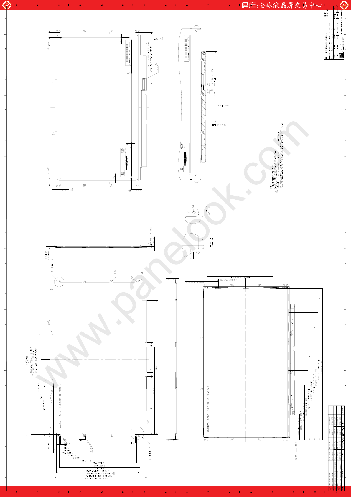
Note (1) Please refer to the attached drawings for more information of front and back outline dimensions.
Vertical(V) 206 206.5 207 mm
Thickness(T) - 3.45 3.65 mm
Weight - 420 435 g
(1)
(1)
(2) Module size doesn’t include hinge.
4 / 28
One step solution for LCD / PDP / OLED panel application: Datasheet, inventory and accessory!
Version 0.0
www.panelook.com
Page 5
Global LCD Panel Exchange Center
A
2. ABSOLUTE MAXIMUM RATINGS
2.1 ABSOLUTE RATINGS OF ENVIRONMENT
Item Symbol
Storage Temperature TST -20 +60 ºC (1)
Operating Ambient Temperature TOP 0 +50 ºC (1), (2)
Shock (Non-Operating) S
Vibration (Non-Operating) V
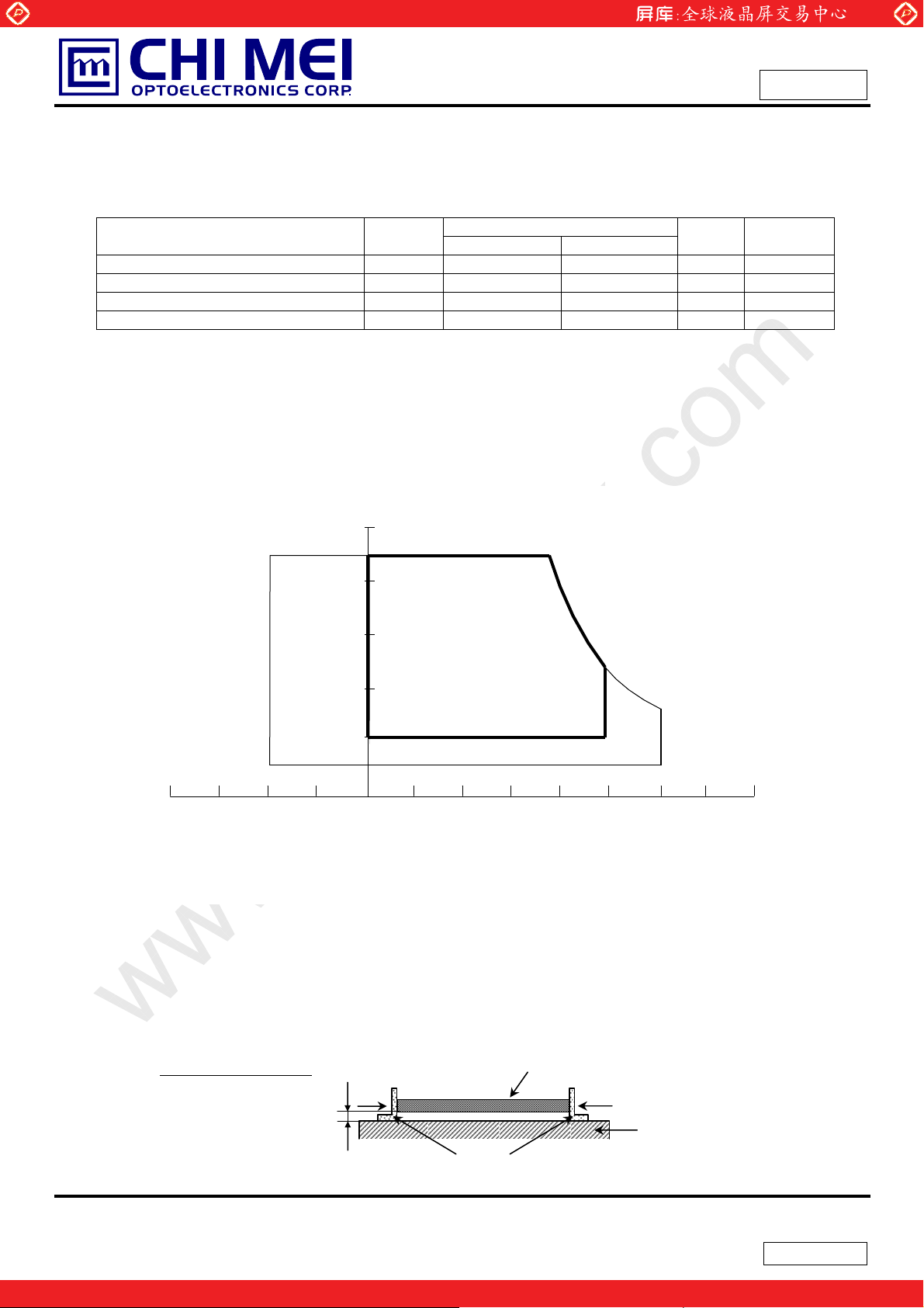
Note (1) Temperature and relative humidity range is shown in the figure below.
(a) 90 %RH Max. (Ta <= 40 ºC).
(b) Wet-bulb temperature should be 39 ºC Max. (Ta > 40 ºC).
(c) No condensation.
Note (2) The temperature of panel surface area should be 0 ºC min. and 60 ºC max.
www.panelook.com
Issued Date :Feb, 17, 2009
Model No.: N156O6-L04
Tentative
Value
Min. Max.
- 220/2 G/ms (3), (5)
NOP
- 1.5 G (4), (5)
NOP
Unit Note
Relative Humidity (%RH)
100
90
80
60
Operating Range
40
20
10
Storage Range
Temperature (ºC)
Note (3) 1 time for ± X, ± Y, ± Z. for Condition (220G / 2ms) is half Sine Wave,.
Note (4) 10~500 Hz, 30 min/cycle, 1cycle for X,Y,Z-axis.
8060-20 40 0 20 -40
Note (5) At testing Vibration and Shock, the fixture in holding the module has to be hard and rigid
enough so that the module would not be twisted or bent by the fixture.
The fixing condition is shown as below:
t Room Temperature
Side Mount Fixing Screw
Gap=2mm
Bracket
LCD Module
Side Mount Fixing Screw
Stage
5 / 28
One step solution for LCD / PDP / OLED panel application: Datasheet, inventory and accessory!
Version 0.0
www.panelook.com
Page 6
Global LCD Panel Exchange Center
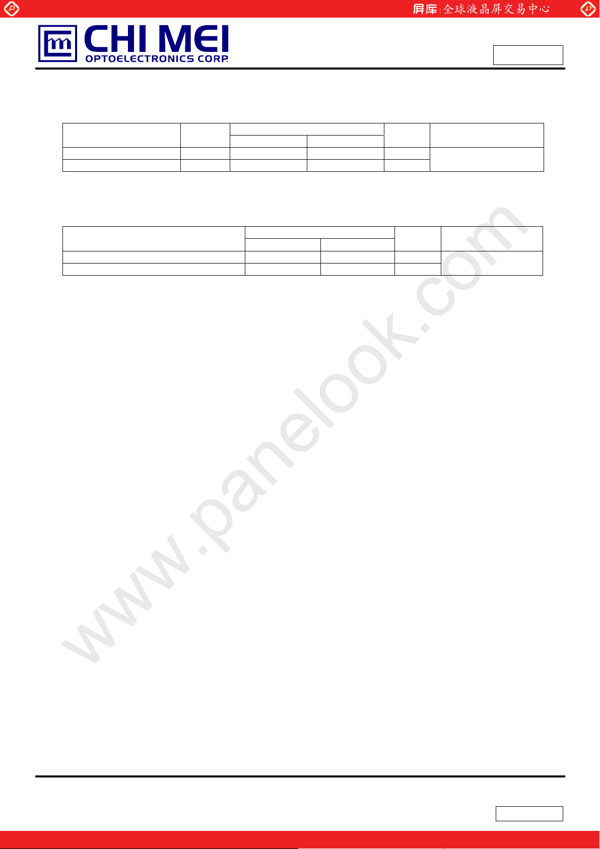
2.2 ELECTRICAL ABSOLUTE RATINGS
2.2.1 TFT LCD MODULE
Item Symbol
Power Supply Voltage Vcc -0.3 +4.0 V
Logic Input Voltage VIN -0.3 Vcc+0.3 V
2.2.2 BACKLIGHT UNIT
Item
LED Light Bar Power Supply Voltage -45 30.6 V
LED Light Bar Power Supply Current 0 150 mA
Note (1) Permanent damage to the device may occur if maximum values are exceeded. Function operation
www.panelook.com
Value
Min. Max.
Value
Min Max.
Unit Note
Issued Date :Feb, 17, 2009
Model No.: N156O6-L04
Tentative
(1)
Unit Note
DC
DC
(1), (2)
should be restricted to the conditions described under Normal Operating Conditions.
Note (2) Specified values are for LED (Refer to Section 3.2 for further information).
6 / 28
One step solution for LCD / PDP / OLED panel application: Datasheet, inventory and accessory!
Version 0.0
www.panelook.com
Page 7
Global LCD Panel Exchange Center
www.panelook.com
Issued Date :Feb, 17, 2009
Model No.: N156O6-L04
3. ELECTRICAL CHARACTERISTICS
3.1 TFT LCD MODULE Ta = 25 ± 2 ºC
Parameter Symbol
Min. Typ. Max.
Power Supply Voltage Vcc 3.0 3.3 3.6 V Ripple Voltage VRP - - mV -
Rush Current I
- - 1.5 A (2)
RUSH
Initial Stage Current IIS - - 1.0 A (2)
Power Supply Current
LVDS Differential Input High Threshold V
LVDS Differential Input Low Threshold V
White - 255 275 mA (3)a
Black
lcc
TH(LVDS)
-100 - - mV
TL(LVDS)
- 355 410 mA (3)b
- - +100 mV
LVDS Common Mode Voltage VCM 1.125 - 1.375 V (5)
LVDS Differential Input Voltage |VID| 100 - 600 mV (5)
Terminating Resistor RT - 100 - Ohm -
Power per EBL WG P
- (2.2) - W (4)
EBL
Note (1) The ambient temperature is Ta = 25 ± 2 ºC.
Value
Unit Note
Tentative
(5),
=1.2V
V
CM
(5)
=1.2V
V
CM
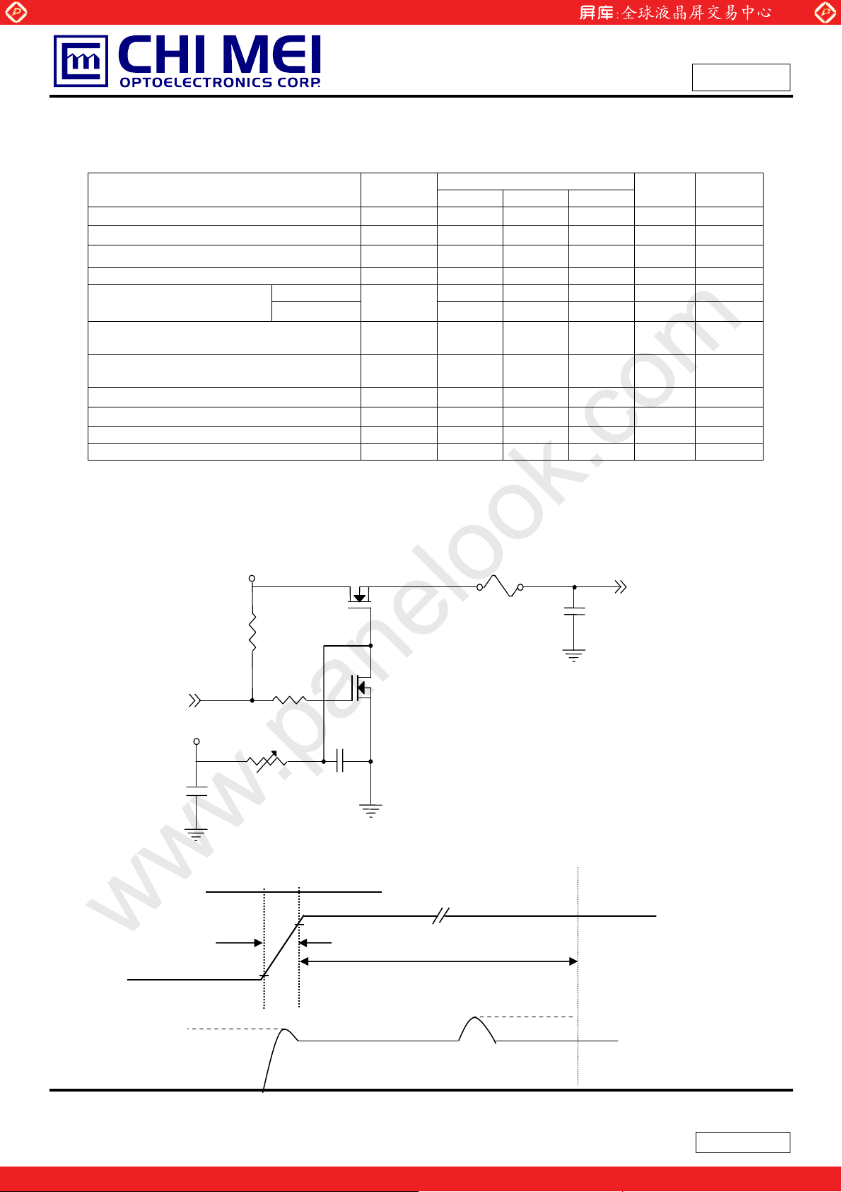
Note (2) I
Measurement Conditions: Shown as the following figure. Test pattern: black.
: the maximum current when VCC is rising
RUSH
I
: the maximum current of the first 100ms after power-on
IS
(High to Low)
(Control Signal)
SW
+12V
+3.3V
R1
47K
R2
1K
47K
VR1
C1
1uF
Q1 2SK1475
Q2
2SK1470
C2
0.01uF
FUSE
C3
1uF
Vcc rising time is 470us
+3.3V
VCC
Vcc
(LCD Module Input)
100ms
I
IS
0V
I
RUSH
470us
0.1Vcc
ICC
7 / 28
One step solution for LCD / PDP / OLED panel application: Datasheet, inventory and accessory!
Version 0.0
www.panelook.com
Page 8
Global LCD Panel Exchange Center
|
|
|
|
Note (3) The specified power supply current is under the conditions at Vcc = 3.3 V, Ta = 25 ± 2 ºC, DC
www.panelook.com
Issued Date :Feb, 17, 2009
Model No.: N156O6-L04
Tentative
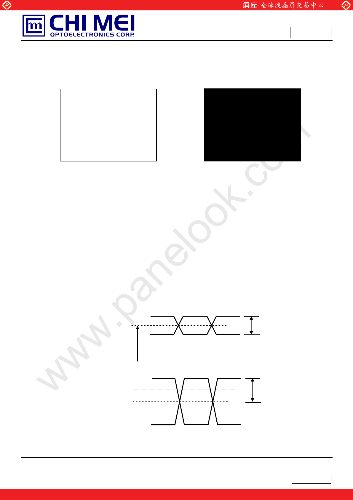
Current and f
a. White Pattern
Note (4) The specified power are the sum of LCD panel electronics input power and the converter input
power. Test conditions are as follows.
(a) Vcc = 3.3 V, Ta = 25 ± 2 ºC, f
(b) The pattern used is a black and white 32 x 36 checkerboard, slide #100 from the VESA file
“Flat Panel Display Monitor Setup Patterns”, FPDMSU.ppt.
= 60 Hz, whereas a power dissipation check pattern below is displayed.
v
b. Black Pattern
Active Area
= 60 Hz,
v
Active Area
(c) Luminance: 60 nits.
Note (5) The parameters of LVDS signals are defined as the following figures.
CM
V
Single Ended
0V
V
Differential
0V
V
VID
VID
8 / 28
One step solution for LCD / PDP / OLED panel application: Datasheet, inventory and accessory!
Version 0.0
www.panelook.com
Page 9
Global LCD Panel Exchange Center
www.panelook.com
Issued Date :Feb, 17, 2009
Model No.: N156O6-L04
3.2 BACKLIGHT UNIT Ta = 25 ± 2 ºC
Parameter Symbol
LED Light Bar input
Voltage
LED Light Bar input
Current
V
L
I
L
Min. Typ. Max.
26.1 28.8 30.6 V
114 120 126 mA
Power Consumption PL 2.975 3.456 3.856 W
LED Life Time LBL 15000 - - Hrs (4)
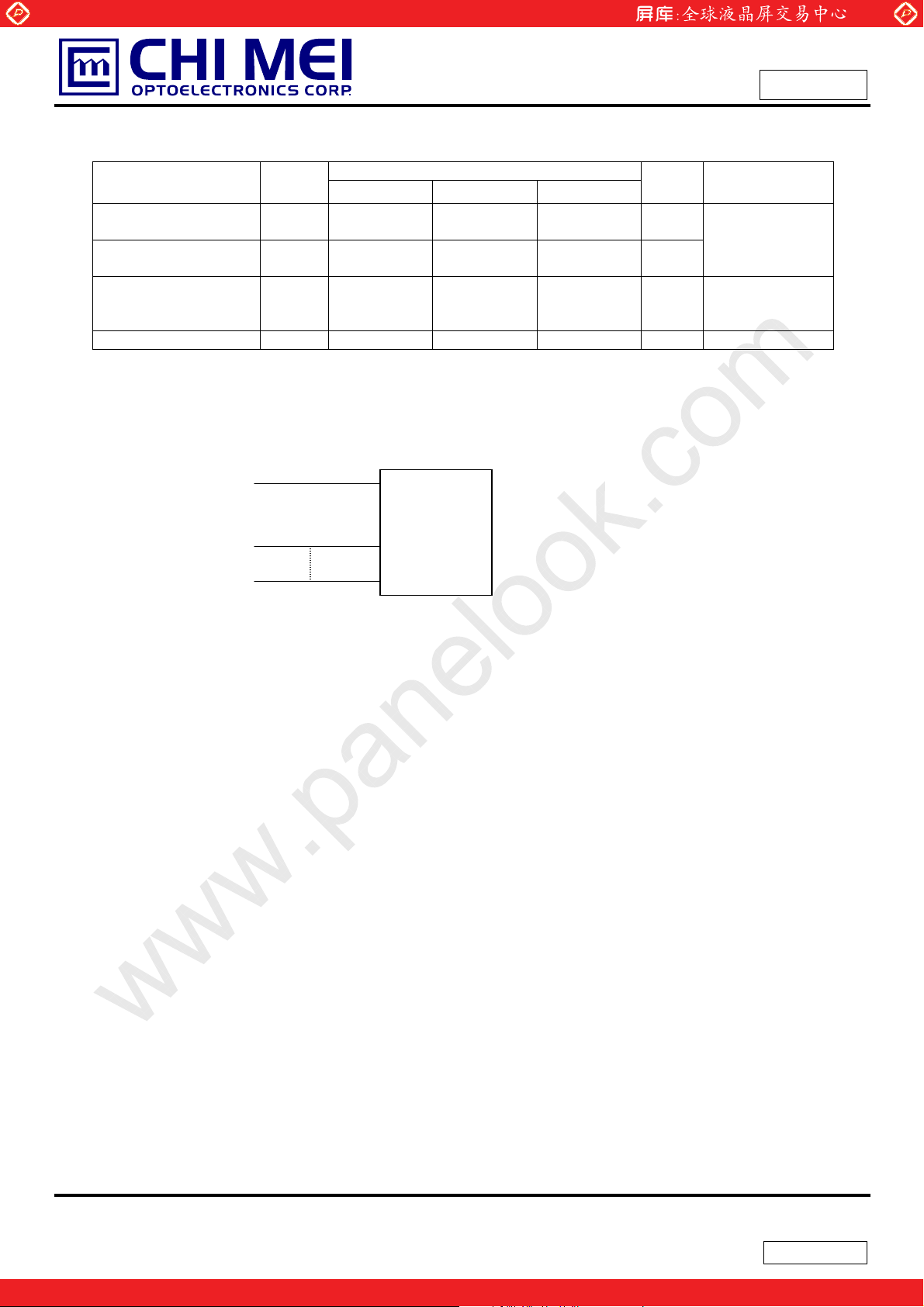
Note (1) LED light bar configuration is shown as below.
VL,I
L
Value
Unit Note
(1) Duty 100%
(3)
=120mA
I
L
Duty=100%
Tentative
LED
Light Bar Feedback
Light Bar
Channels
Note (2) For better LED light bar driving quality, it is recommended to utilize the adaptive boost converter
with current balancing function to drive LED light-bar.
Note (3) P
= ILØ V
L
L
Note (4) The lifetime of LED is defined as the time when it continues to operate under the conditions at Ta = 2 5 ± 2oC and
I
= 20.0 mA(Per EA) until the brightness becomes 50% of its original value.Љ
L
9 / 28
One step solution for LCD / PDP / OLED panel application: Datasheet, inventory and accessory!
Version 0.0
www.panelook.com
Page 10
Global LCD Panel Exchange Center
4. BLOCK DIAGRAM--EE
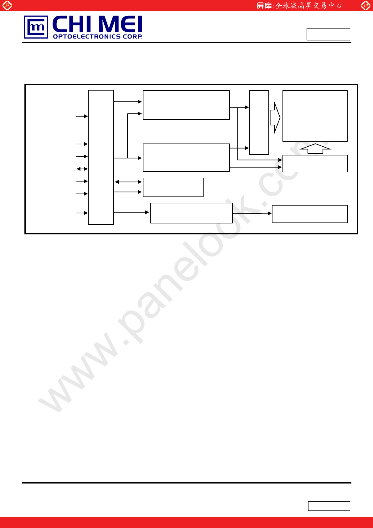
4.1 TFT LCD MODULE
www.panelook.com
Issued Date :Feb, 17, 2009
Model No.: N156O6-L04
Tentative
LVDS Display
Data & Clock
Vcc
GND
Data
EDID
CLK
EDID
V
EDID
LED Power & Signal
INPUT CONNECTOR
LVDS INPUT /
TIMING CONTROLLER
DC/DC CONVERTER &
REFERENCE VOLTAGE
GENERATOR
EDID
EEPROM
LED
Converter
SCAN DRIVER IC
TFT LCD PANEL
(1600x3x900)
DATA DRIVER IC
BACKLIGHT UNIT
10 / 28
One step solution for LCD / PDP / OLED panel application: Datasheet, inventory and accessory!
Version 0.0
www.panelook.com
Page 11
Global LCD Panel Exchange Center
5. INPUT TERMINAL PIN ASSIGNMENT--EE
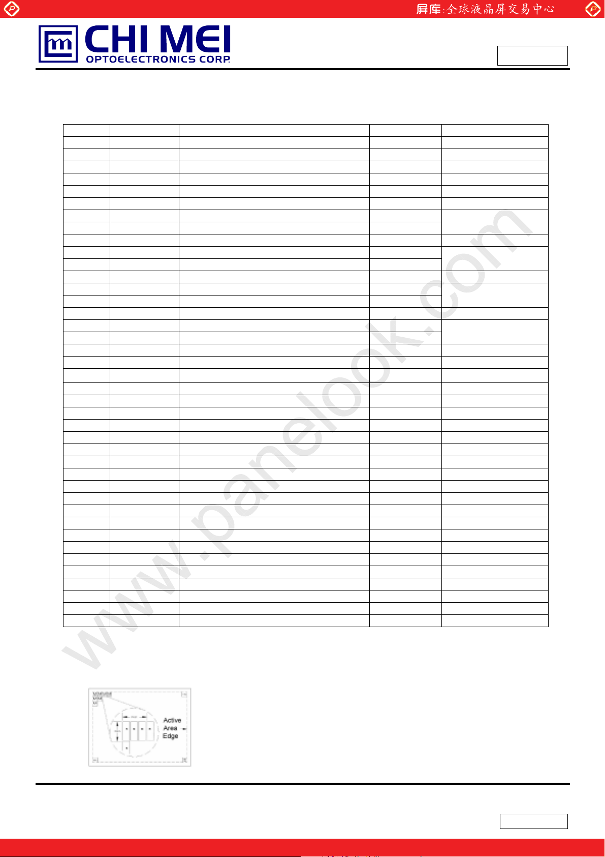
5.1 TFT LCD MODULE
Pin Symbol Description Polarity Remark
1 NC No Connection
2 AVDD Power Supply, 3.3V (typical)
3 AVDD Power Supply, 3.3V (typical)
4 DVDD DDC 3.3V power
5 NC No Connect
6 SCL DDC Clock
7 SDA DDC Data
8 RXO0- LVDS Differential Data Input (Odd) Negative
9 RXO0+ LVDS Differential Data Input (Odd) Positive
10 Vss Ground
11 RXO1- LVDS Differential Data Input (Odd) Negative
12 RXO1+ LVDS Differential Data Input (Odd) Positive
13 Vss Ground
14 RXO2- LVDS Differential Data Input (Odd) Negative
15 RXO2+ LVDS Differential Data Input (Odd) Positive
16 Vss Ground
17 RXOC- LVDS Clock Data Input (Odd) Negative
18 RXOC+ LVDS Clock Data Input (Odd) Positive
19 Vss Ground
20 RxE0- LVDS Differential Data Input (Even) Negative
21 RxE0+ LVDS Differential Data Input (Even) Positive
22 Vss Ground
23 RxE1- LVDS Differential Data Input (Even) Negative
24 RxE1+ LVDS Differential Data Input (Even) Positive
25 Vss Ground
26 RxE2- LVDS Differential Data Input (Even) Negative
27 RxE2+ LVDS Differential Data Input (Even) Positive
28 Vss Ground
29 RXEC- LVDS Clock Data Input (Even) Negative
30 RXEC+ LVDS Clock Data Input (Even) Positive
31 LED_GND LED Ground
32 LED_GND LED Ground
33 LED_GND LED Ground
34 NC No Connection
35 LED_PWM PWM Control Signal of LED Converter
36 LED_EN Enable Control Signal of LED Converter
37 NC No Connection
38 LED_VCCS LED Power
39 LED_VCCS LED Power
40 LED_VCCS LED Power
Note (1) Connector Part No.: I-PEX 20455-040E-12 or equivalent
www.panelook.com
Issued Date :Feb, 17, 2009
Model No.: N156O6-L04
Tentative
Note (2) User’s connector Part No: I-PEX 20453-040T-01 or equivalent
Note (3) The first pixel is odd as shown in the following figure.
11 / 28
One step solution for LCD / PDP / OLED panel application: Datasheet, inventory and accessory!
Version 0.0
www.panelook.com
Page 12
Global LCD Panel Exchange Center
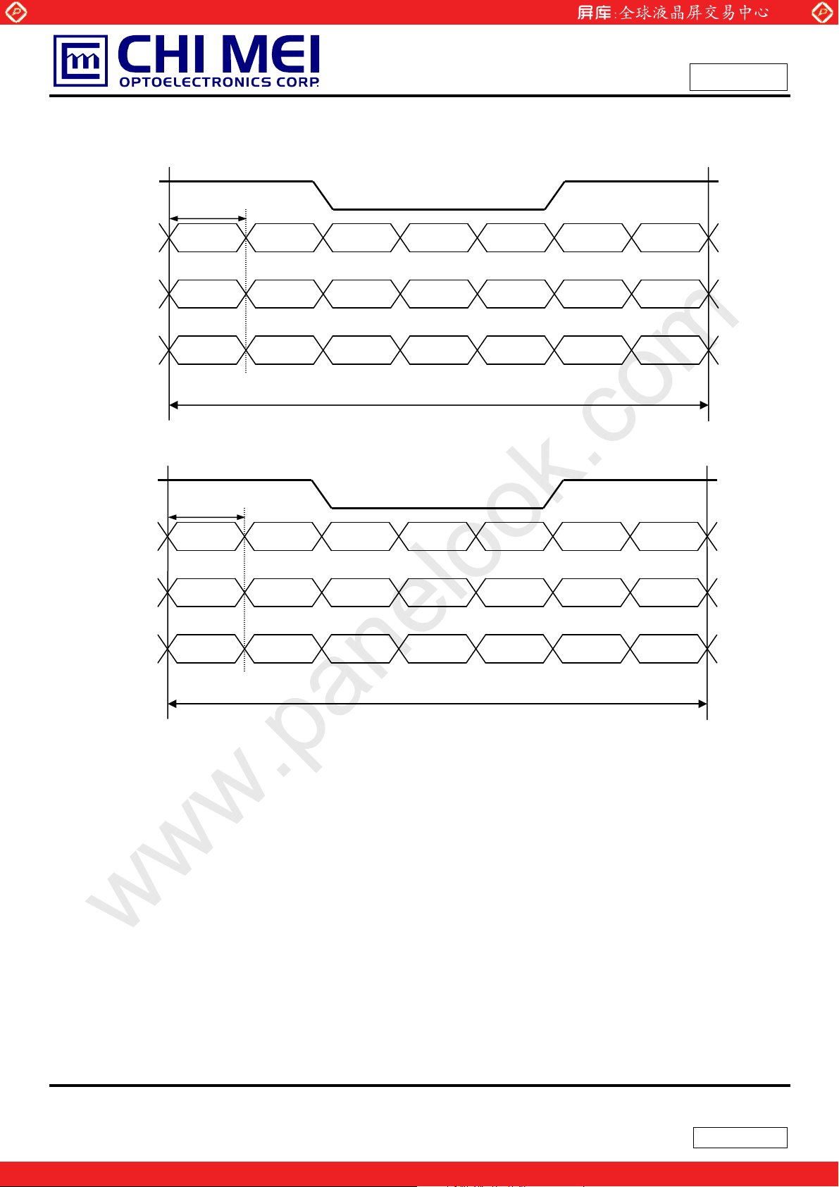
5.2 TIMING DIAGRAM OF LVDS INPUT SIGNAL
RXOC+
T/7
www.panelook.com
Issued Date :Feb, 17, 2009
Model No.: N156O6-L04
Tentative
RXO2+/-
RXO1+/-
RXO0+/-
RXEC+
RXE2+/-
RXE1+/-
IN20 IN19 IN18 IN17 IN16 IN15 IN14
DE OB5 OB4 OB3 OB2 Vsync Hsync
IN13 IN12 IN11 IN10 IN9 IN8 IN7
OB1 OG4 OG3 OG2 OG1 OB0 OG5
IN6 IN5 IN4 IN3 IN2 IN1 IN0
OG0 OR3 OR2 OR1 OR0 OR5 OR4
Signal for 1 DCLK Cycle (T)
T/7
IN20 IN19 IN18 IN17 IN16 IN15 IN14
DE EB5 EB4 EB3 EB2 Vsync Hsync
IN13 IN12 IN11 IN10 IN9 IN8 IN7
EB1 EG4 EG3 EG2 EG1 EB0 EG5
RXE0+/-
IN6 IN5 IN4 IN3 IN2 IN1 IN0
EG0 ER3 ER2 ER1 ER0 ER5 ER4
Signal for 1 DCLK Cycle (T)
12 / 28
One step solution for LCD / PDP / OLED panel application: Datasheet, inventory and accessory!
Version 0.0
www.panelook.com
Page 13
Global LCD Panel Exchange Center
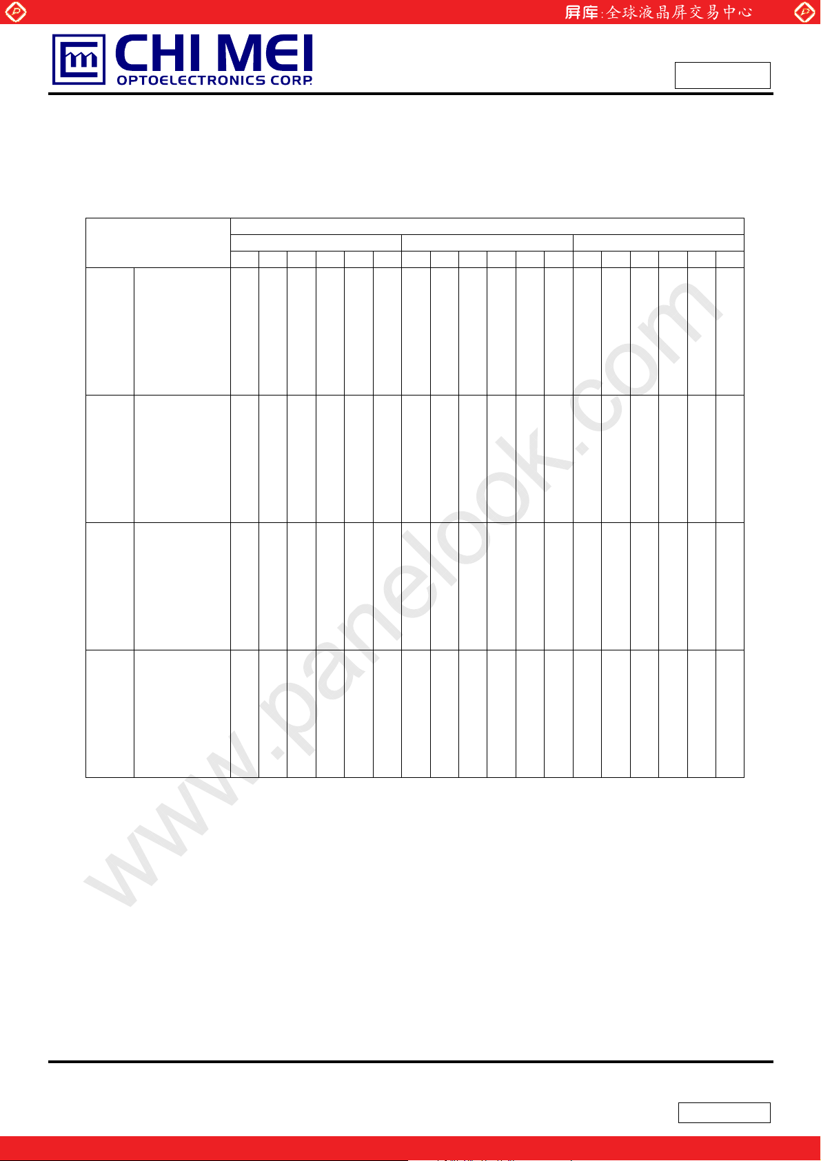
5.3 COLOR DATA INPUT ASSIGNMENT
The brightness of each primary color (red, green and blue) is based on the 6-bit gray scale data input for
the color. The higher the binary input the brighter the color. The table below provides the assignment of
color versus data input.
Color
R5 R4 R3 R2 R1 R0 G5 G4 G3 G2 G1 G0 B5 B4 B3 B2 B1 B0
Black
Red
Green
Basic
Colors
Gray
Scale
Of
Red
Gray
Scale
Of
Green
Gray
Scale
Of
Blue
Note (1) 0: Low Level Voltage, 1: High Level Voltage
Blue
Cyan
Magenta
Yellow
White
Red(0)/Dark
Red(1)
Red(2)
:
:
Red(61)
Red(62)
Red(63)
Green(0)/Dark
Green(1)
Green(2)
:
:
Green(61)
Green(62)
Green(63)
Blue(0)/Dark
Blue(1)
Blue(2)
:
:
Blue(61)
Blue(62)
Blue(63)
0
0
1
1
0
0
0
0
0
0
1
1
1
1
1
1
0
0
0
0
0
0
:
:
:
:
1
1
1
1
1
1
0
0
0
0
0
0
:
:
:
:
0
0
0
0
0
0
0
0
0
0
0
0
:
:
:
:
0
0
0
0
0
0
www.panelook.com
Issued Date :Feb, 17, 2009
Model No.: N156O6-L04
Tentative
Data Signal
Red Green Blue
0
0
0
0
0
0
0
0
0
0
0
0
0
0
0
0
1
1
1
1
0
0
0
0
0
0
0
0
0
0
0
0
0
0
0
0
1
1
1
1
1
1
0
0
0
0
0
0
0
0
0
0
0
0
0
0
0
0
1
1
1
1
1
1
0
0
0
0
1
1
1
1
1
1
1
1
1
1
1
1
1
1
1
1
0
0
0
0
0
0
1
1
1
1
1
1
1
1
1
1
1
1
1
1
1
1
0
0
0
0
0
0
1
1
1
1
1
1
1
1
1
1
1
1
1
1
1
1
0
0
0
0
0
0
0
0
0
0
0
0
0
0
0
0
0
0
0
1
0
0
0
0
0
0
0
0
0
0
0
0
0
0
1
0
0
0
0
0
0
0
0
0
0
0
0
0
:
:
:
:
:
:
:
:
:
:
:
:
:
:
:
:
:
:
:
:
:
:
:
:
:
:
:
:
:
:
:
:
1
1
0
1
0
0
0
0
0
0
0
0
0
0
0
0
1
1
1
0
0
0
0
0
0
0
0
0
0
0
0
0
1
1
1
1
0
0
0
0
0
0
0
0
0
0
0
0
0
0
0
0
0
0
0
0
0
0
0
0
0
0
0
0
0
0
0
0
0
0
0
0
0
1
0
0
0
0
0
0
0
0
0
0
0
0
0
0
1
0
0
0
0
0
0
0
:
:
:
:
:
:
:
:
:
:
:
:
:
:
:
:
:
:
:
:
:
:
:
:
:
:
:
:
:
:
:
:
0
0
0
0
1
1
1
1
0
1
0
0
0
0
0
0
0
0
0
0
1
1
1
1
1
0
0
0
0
0
0
0
0
0
0
0
1
1
1
1
1
1
0
0
0
0
0
0
0
0
0
0
0
0
0
0
0
0
0
0
0
0
0
0
0
0
0
0
0
0
0
0
0
0
0
0
0
0
0
1
0
0
0
0
0
0
0
0
0
0
0
0
0
0
1
0
:
:
:
:
:
:
:
:
:
:
:
:
:
:
:
:
:
:
:
:
:
:
:
:
:
:
:
:
:
:
:
:
0
0
0
0
0
0
0
0
0
0
1
1
1
1
0
1
0
0
0
0
0
0
0
0
0
0
1
1
1
1
1
0
0
0
0
0
0
0
0
0
0
0
1
1
1
1
1
1
13 / 28
One step solution for LCD / PDP / OLED panel application: Datasheet, inventory and accessory!
Version 0.0
www.panelook.com
Page 14
Global LCD Panel Exchange Center
www.panelook.com
Issued Date :Feb, 17, 2009
Model No.: N156O6-L04
Tentative
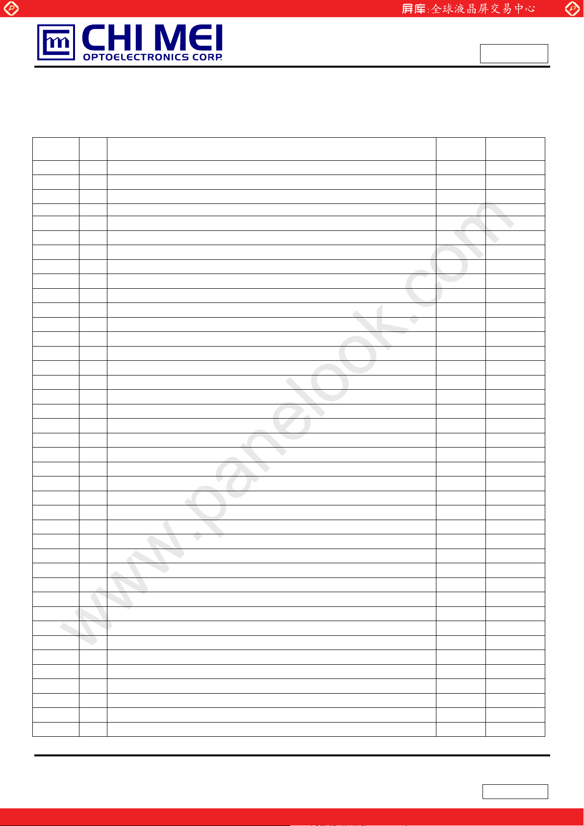
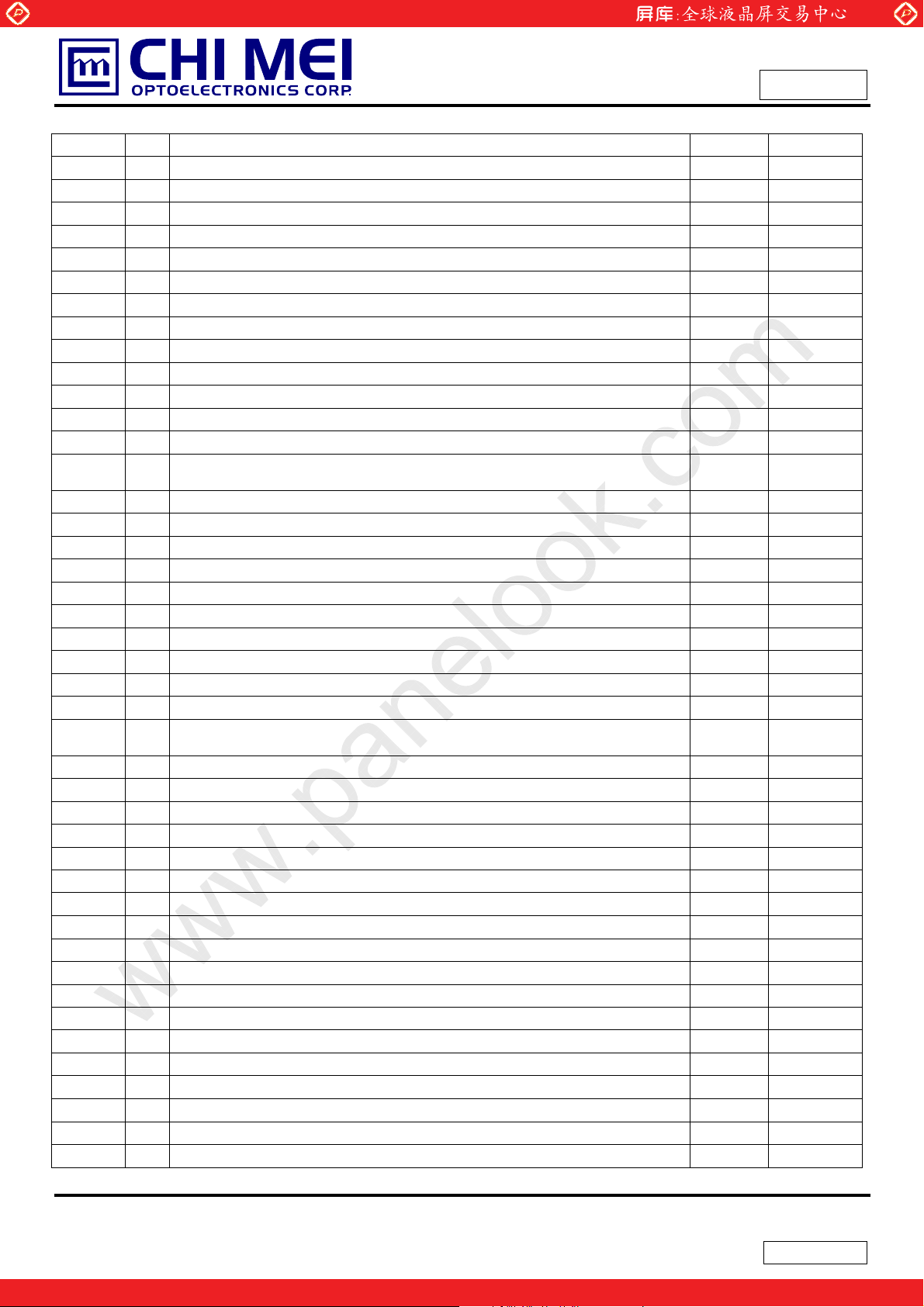
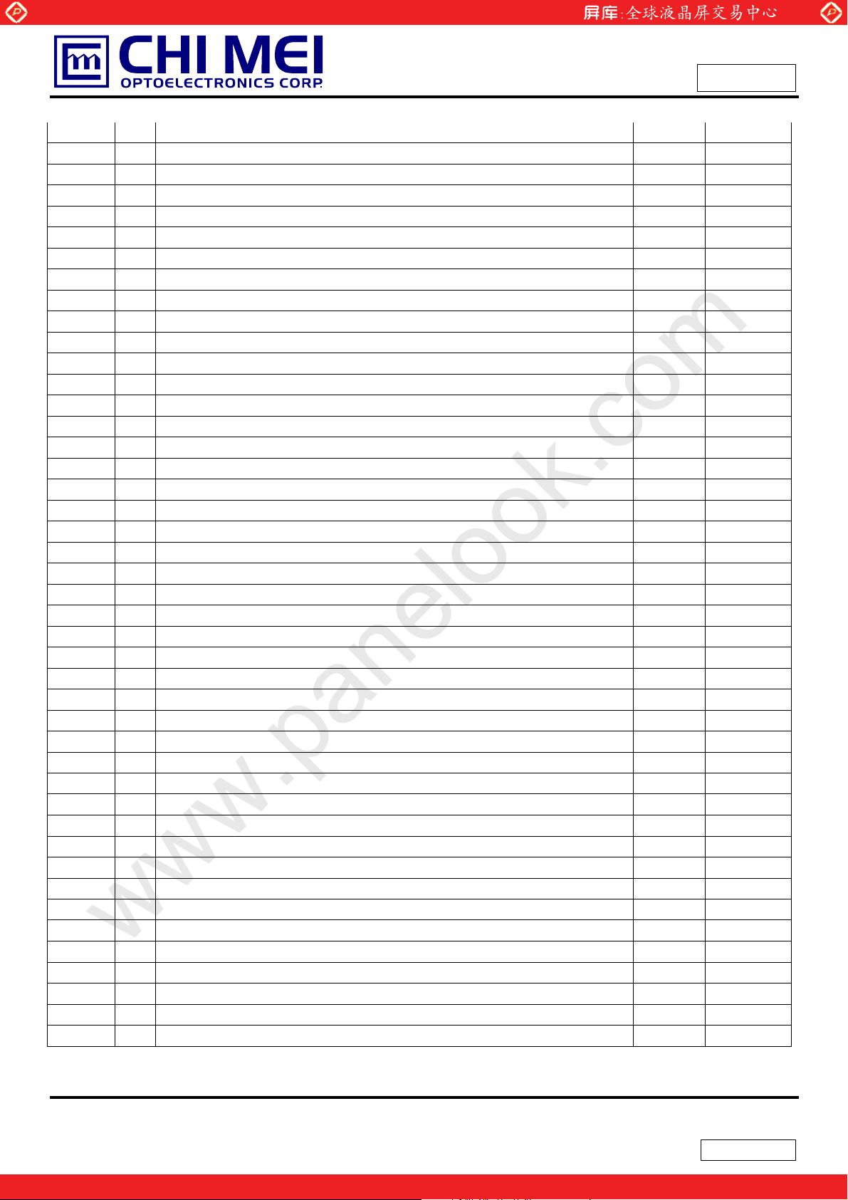
5.4 EDID DATA STRUCTURE--EE
The EDID (Extended Display Identification Data) data formats are to support displays as defined in the
VESA Plug & Display and FPDI standards.
Byte
#(decimal)
0 0 Header
1 1 Header
2 2 Header
3 3 Header
4 4 Header
5 5 Header
6 6 Header
7 7 Header
8 8 EISA ID manufacturer name (“CMO”)
9 9 EISA ID manufacturer name (Compressed ASCII)
10 0A ID product code (N156O6-L04) 79
11 0B ID product code (hex LSB first; N156O6-L04) 15
12 0C ID S/N (fixed “0”)
13 0D ID S/N (fixed “0”)
14 0E ID S/N (fixed “0”)
15 0F ID S/N (fixed “0”)
16 10 Week of manufacture (fixed week code)
17 11 Year of manufacture (fixed year code)
18 12 EDID structure version # (“1”)
19 13 EDID revision # (“3”)
20 14 Video I/P definition (“digital”)
21 15 Active area horizontal 34.416cm
22 16 Active area vertical 19.359cm
23 17 Display Gamma (Gamma = ”2.2”)
24 18 Feature support (“Active off, RGB Color”)
25 19 Rx1, Rx0, Ry1, Ry0, Gx1, Gx0, Gy1, Gy0 87
26 1A Bx1, Bx0, By1, By0, Wx1, Wx0, Wy1, Wy0 F5
27 1B Rx=0.58 94
28 1C Ry=0.34 57
29 1D Gx=0.31 4F
30 1E Gy=0.55 8C
31 1F Bx=0.155 27
32 20 By=0.155 27
33 21 Wx=0.313 50
34 22 Wy=0.329 54
35 23 Established timings 1
36 24 Established timings 2
37 25 Manufacturer’s reserved timings
38 26 Standard timing ID # 1
39 27 Standard timing ID # 1
Byte
#(hex)Field Name and Comments Value(hex) Value(binary)
00 00000000
FF 11111111
FF 11111111
FF 11111111
FF 11111111
FF 11111111
FF 11111111
00 00000000
0D 00001101
AF 10101111
00 00000000
00 00000000
00 00000000
00 00000000
29 00101001
12 00010010
01 00000001
03 00000011
80 10000000
22 00100010
13 00010011
78 01111000
0A 00001010
00 00000000
00 00000000
00 00000000
01 00000001
01 00000001
01111001
00010101
10000111
11110101
10010100
01010111
01001111
10001100
00100111
00100111
01010000
01010100
14 / 28
One step solution for LCD / PDP / OLED panel application: Datasheet, inventory and accessory!
Version 0.0
www.panelook.com
Page 15
Global LCD Panel Exchange Center
www.panelook.com
Issued Date :Feb, 17, 2009
Model No.: N156O6-L04
Tentative
40 28 Standard timing ID # 2
41 29 Standard timing ID # 2
42 2A Standard timing ID # 3
43 2B Standard timing ID # 3
44 2C Standard timing ID # 4
45 2D Standard timing ID # 4
46 2E Standard timing ID # 5
47 2F Standard timing ID # 5
48 30 Standard timing ID # 6
49 31 Standard timing ID # 6
50 32 Standard timing ID # 7
51 33 Standard timing ID # 7
52 34 Standard timing ID # 8
53 35 Standard timing ID # 8
Detailed timing description # 1 Pixel clock (“97.75MHz”, According to VESA
54 36
55 37 # 1 Pixel clock (hex LSB first)
56 38 # 1 H active (“1600”)
57 39 # 1 H blank (“160”)
58 3A # 1 H active : H blank (“1600 : 160”)
59 3B # 1 V active (”900”)
60 3C # 1 V blank (”26”)
61 3D # 1 V active : V blank (”900 :26”)
62 3E # 1 H sync offset (”48”)
63 3F # 1 H sync pulse width ("32”)
64 40 # 1 V sync offset : V sync pulse width (”3 : 5”)
65 41
66 42 # 1 H image size (”344 mm”) 58
67 43 # 1 V image size (”193 mm”) C1
68 44 # 1 H image size : V image size (”344 : 193”)
69 45 # 1 H boarder (”0”)
70 46 # 1 V boarder (”0”)
71 47 # 1 Non-interlaced, Normal, no stereo, Separate sync, H/V pol Negatives
72 48 Detailed timing description # 2
73 49 # 2 Flag
74 4A # 2 Reserved
75 4B # 2 FE (hex) defines ASCII string (Model Name “N156O6-L01”, ASCII)
76 4C # 2 Flag
77 4D # 2 1st character of name (“N”)
78 4E # 2 2nd character of name (“1”)
79 4F # 2 3rd character of name (“5”)
80 50 # 2 4th character of name (“6”)
81 51 # 2 5th character of name (“O”)
82 52 # 2 6th character of name (“6”)
83 53 # 2 7th character of name (“-”)
CVT Rev1.1)
# 1 H sync offset : H sync pulse width : V sync offset : V sync width (”48:
32 : 3 : 5”)
01 00000001
01 00000001
01 00000001
01 00000001
01 00000001
01 00000001
01 00000001
01 00000001
01 00000001
01 00000001
01 00000001
01 00000001
01 00000001
01 00000001
2F 00101111
26 00100110
40 01000000
A0 10100000
60 01100000
84 10000100
1A 00011010
30 00110000
30 00110000
20 00100000
35 00110101
00 00000000
10 00010000
00 00000000
00 00000000
18 00011000
00 00000000
00 00000000
00 00000000
FE 11111110
00 00000000
4E 01001110
31 00110001
35 00110101
36 00110110
4F 01001111
36 00110110
2D 00101101
01011000
11000001
15 / 28
One step solution for LCD / PDP / OLED panel application: Datasheet, inventory and accessory!
Version 0.0
www.panelook.com
Page 16
Global LCD Panel Exchange Center
www.panelook.com
Issued Date :Feb, 17, 2009
Model No.: N156O6-L04
Tentative
84 54 # 2 8th character of name (“L”)
85 55 # 2 9th character of name (“0”)
86 56 # 2 9th character of name (“4”)
87 57 # 2 New line character indicates end of ASCII string
88 58 # 2 Padding with “Blank” character
89 59 # 2 Padding with “Blank” character
90 5A Detailed timing description # 3
91 5B # 3 Flag
92 5C # 3 Reserved
93 5D # 3 FE (hex) defines ASCII string (Vendor “CMO”, ASCII)
94 5E # 3 Flag
95 5F # 3 1st character of string (“C”)
96 60 # 3 2nd character of string (“M”)
97 61 # 3 3rd character of string (“O”)
98 62 # 3 New line character indicates end of ASCII string
99 63 # 3 Padding with “Blank” character
100 64 # 3 Padding with “Blank” character
101 65 # 3 Padding with “Blank” character
102 66 # 3 Padding with “Blank” character
103 67 # 3 Padding with “Blank” character
104 68 # 3 Padding with “Blank” character
105 69 # 3 Padding with “Blank” character
106 6A # 3 Padding with “Blank” character
107 6B # 3 Padding with “Blank” character
108 6C Detailed timing description # 4
109 6D # 4 Flag
110 6E # 4 Reserved
111 6F # 4 FE (hex) defines ASCII string (Model Name“N156O6-L01”, ASCII)
112 70 # 4 Flag
113 71 # 4 1st character of name (“N”) 4E
114 72 # 4 2nd character of name (“1”) 31
115 73 # 4 3rd character of name (“5”) 35
116 74 # 4 4th character of name (“6”) 36
117 75 # 4 5th character of name (“O”) 4F
118 76 # 4 6th character of name (“6”) 36
119 77 # 4 7th character of name (“-”) 2D
120 78 # 4 8th character of name (“L”) 4C
121 79 # 4 9th character of name (“0”)
122 7A # 4 9th character of name (“4”)
123 7B # 4 New line character indicates end of ASCII string
124 7C # 4 Padding with “Blank” character
125 7D # 4 Padding with “Blank” character
126 7E Extension flag
127 7F Checksum
4C 01001100
30 00110000
34 00110100
0A 00001010
20 00100000
20 00100000
00 00000000
00 00000000
00 00000000
FE 11111110
00 00000000
43 01000011
4D 01001101
4F 01001111
0A 00001010
20 00100000
20 00100000
20 00100000
20 00100000
20 00100000
20 00100000
20 00100000
20 00100000
20 00100000
00 00000000
00 00000000
00 00000000
FE 11111110
00 00000000
30 00110000
34 00110100
0A 00001010
20 00100000
20 00100000
00 00000000
AA 10101010
01001110
00110001
00110101
00110110
01001111
00110110
00101101
01001100
16 / 28
One step solution for LCD / PDP / OLED panel application: Datasheet, inventory and accessory!
Version 0.0
www.panelook.com
Page 17
Global LCD Panel Exchange Center
www.panelook.com
Issued Date :Feb, 17, 2009
Model No.: N156O6-L04
6. CONVERTER SPECIFICATION
6.1 ABSOLUTE MAXIMUM RATINGS
Symbol Ratings
Vin 40.0V
Gnd +/-0.3V
PWM, EN -0.3V~6.0V
6.2 RECOMMENDED OPERATING RATINGS
Parameter Symbol
Min. Typ. Max.
Converter Input power supply voltage Vin 6 12.0 21.0 V
EN Control Level
PWM Control Level
Backlight on 1.6 --- 5.5 V
Backlight off 0 --- 0.8 V
PWM High Level 1.3 --- 5.5 V
PWM Low Level 0 --- 0.15 V
PWM Control Duty Ratio 20 100 %
PWM Control Frequency f
Converter Input Current
Vin=6V 745 820 mA (1)
Vin=21V
190 210 230 Hz
PWM
I
BL
200 220 mA (2)
Note (1) The specified LED power supply current is under the conditions at Vin = 6V, Ta = 25 ± 2 ºC, f
200 Hz, Duty=100%.
Value
Tentative
Unit Note
=
PWM
Note (2) The specified LED power supply current is under the conditions at Vin = 21V, Ta = 25 ± 2 ºC, f
PWM
= 200 Hz, Duty=100%.
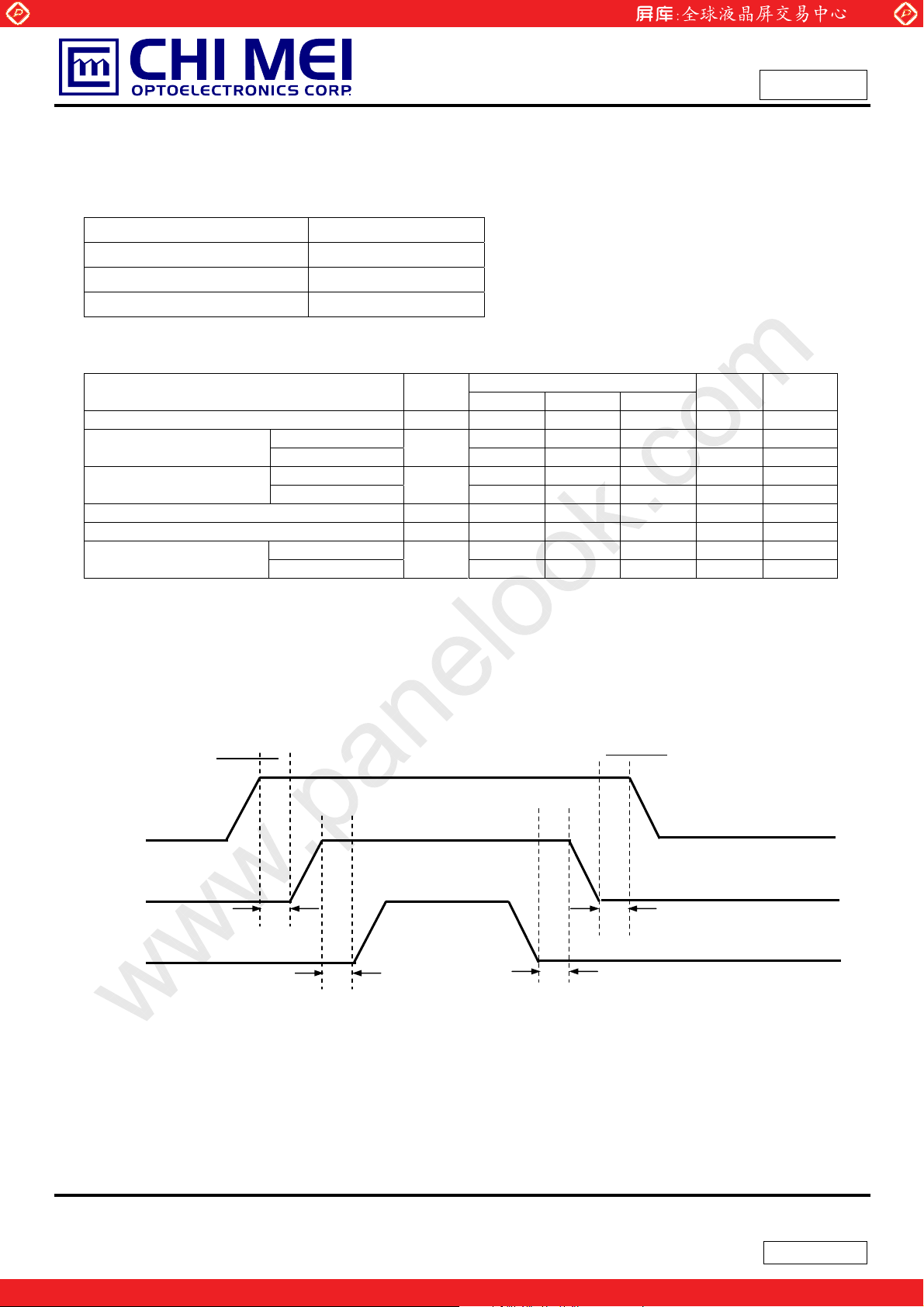
6.3 LED BACKLIGHT CONTROLL POWER SEQUENCE
Power On
LED_VCCS
0V
LED_PWM
0V
T
A
LED_EN
Timing Specifications:
0V
T
Њ( 0ms)
A
T
Њ (0ms)
B
T
Њ (10ms)
C
T
Њ (0ms)
D
T
T
C
D
Note (1) Please follow the LED backlight power sequence as above. If the customer could not follow, it might cause
Power Off
T
B
backlight flash issue during display ON/OFF or damage the LED backlight controller
17 / 28
One step solution for LCD / PDP / OLED panel application: Datasheet, inventory and accessory!
Version 0.0
www.panelook.com
Page 18
Global LCD Panel Exchange Center
7.INTERFACE TIMING--EE
7.1 INPUT SIGNAL TIMING SPECIFICATIONS
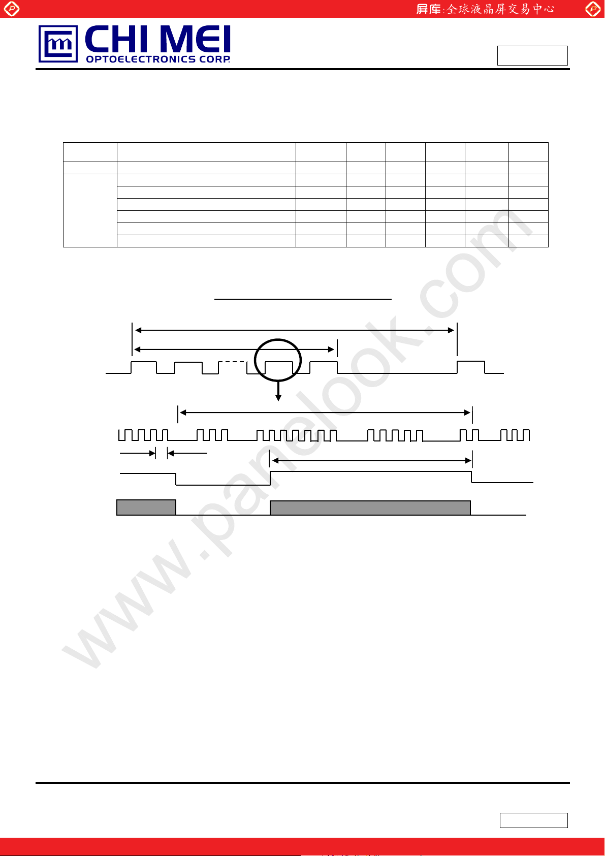
The input signal timing specifications are shown as the following table and timing diagram.
Signal Item Symbol Min. Typ. Max. Unit Note
DCLK Frequency 1/Tc 32.5 48.875 53.8 MHz (2)
Vertical Total Time TV TBD 926 TBD TH -
Vertical Active Display Period TVD TBD 900 TBD TH -
DE
Note (1) Because this module is operated by DE only mode, Hsync and Vsync are ignored.
(2) 2 channels LVDS input.
Vertical Active Blanking Period TVB TV-TVD 26 TV-TVD TH
Horizontal Total Time TH TBD 1760 TBD Tc (2)
Horizontal Active Display Period THD TBD 1600 TBD Tc (2)
Horizontal Active Blanking Period THB
www.panelook.com
TH-THD
INPUT SIGNAL TIMING DIAGRAM
160
Issued Date :Feb, 17, 2009
Model No.: N156O6-L04
Tentative
TH-THD
Tc (2)
DE
DCLK
DE
DATA
TC
HD
T
18 / 28
One step solution for LCD / PDP / OLED panel application: Datasheet, inventory and accessory!
Version 0.0
www.panelook.com
Page 19
Global LCD Panel Exchange Center
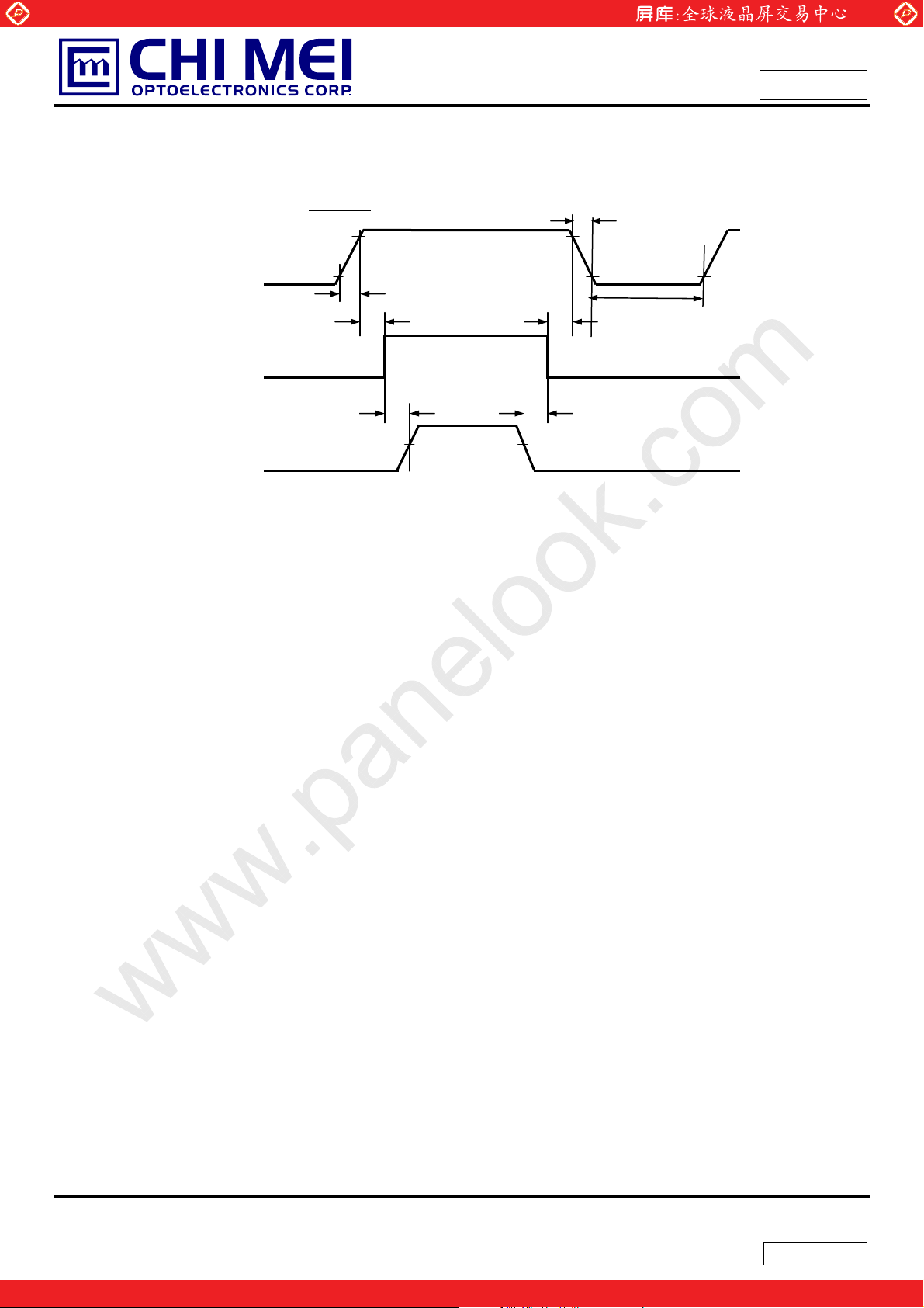
7.2 POWER ON/OFF SEQUENCE
www.panelook.com
Issued Date :Feb, 17, 2009
Model No.: N156O6-L04
Tentative
- Power Supply
for LCD, Vcc
- Interface Signal
(LVDS Signal of
Transmitter), V
I
- Power for Backlight
Timing Specifications:
0.5< t1 <= 10 msec
0 < t2 <= 50 msec
0 < t3 <= 50 msec
t4 >= 500 msec
0V
0V
Power On
90%
10%
10%
Restart
10%
t4
Power Off
t7
90%
t1
t3t2
Valid Data
t6t5
50%50%
ONOFF OFF
t5 >= 200 msec
t6 >= 200 msec
Note (1) Please follow the power on/off sequence described above. Otherwise, the LCD module might be
damaged.
Note (2) Please avoid floating state of interface signal at invalid period. When the interface signal is invalid, be
sure to pull down the power supply of LCD Vcc to 0 V.
Note (3) The Backlight converter power must be turned on after the power supply for the logic and the
interface signal is valid. The Backlight converter power must be turned off before the power supply
for the logic and the interface signal is invalid.
Note (4) Sometimes some slight noise shows when LCD is turned off (even backlight is already off). To
avoid this phenomenon, we suggest that the Vcc falling time is better to follow 50uSЉt7Љ10 ms.
19 / 28
One step solution for LCD / PDP / OLED panel application: Datasheet, inventory and accessory!
Version 0.0
www.panelook.com
Page 20
Global LCD Panel Exchange Center
8. OPTICAL CHARACTERISTICS--OPT
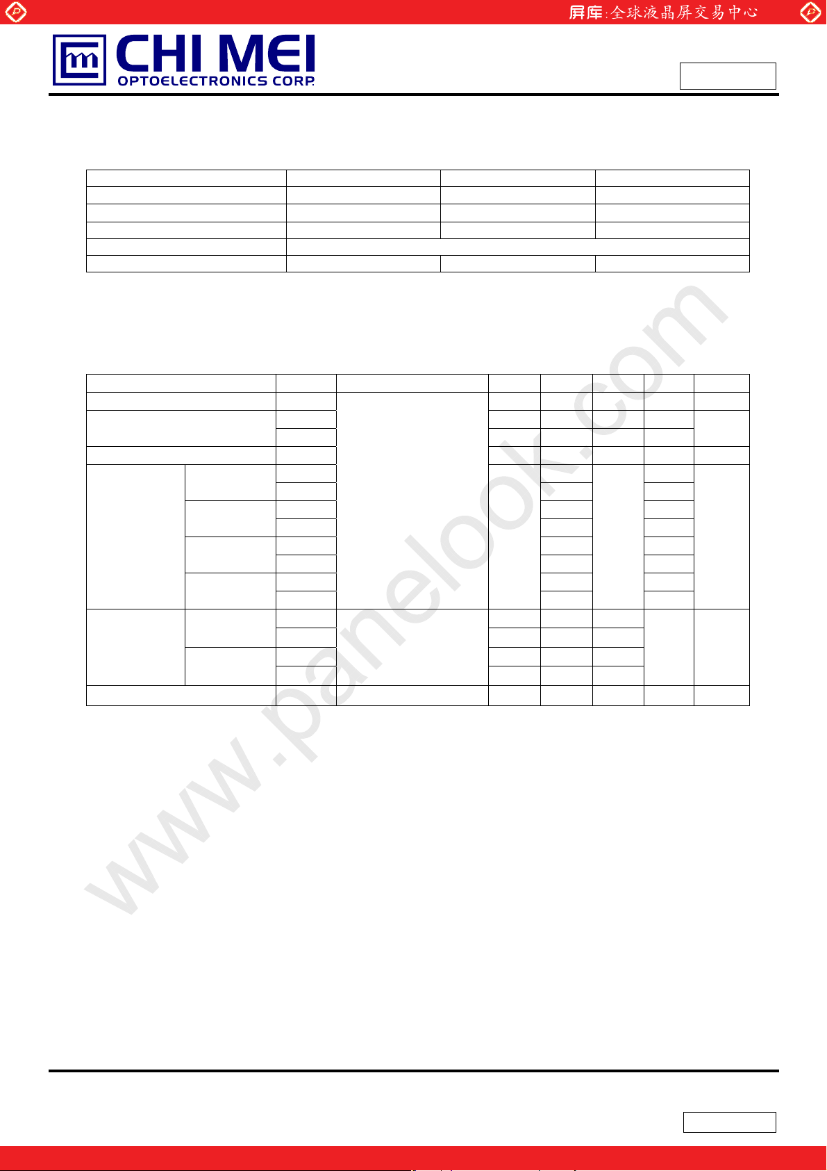
8.1 TEST CONDITIONS
Item Symbol Value Unit
Ambient Temperature Ta
Ambient Humidity Ha
Supply Voltage VCC 3.3 V
Input Signal According to typical value in "3. ELECTRICAL CHARACTERISTICS"
LED Light Bar Input Current IL (120) mA
The measurement methods of optical characteristics are shown in Section 8.2. The following items should
be measured under the test conditions described in Section 8.1 and stable environment shown in Note (5).
8.2 OPTICAL SPECIFICATIONS
Item Symbol Condition Min. Typ. Max. Unit Note
Contrast Ratio CR 500 650 - - (2), (5)
Response Time
Average Luminance of White
Red
Color
Chromaticity
Green
Blue
White
Horizontal
Viewing Angle
Vertica l
White Variation of 5 Points δW
TR - 3 8 ms
T
F
L
AVE
Rx
Ry
Gx
Gy
Bx
By
Wx 0.313 Wy
θx+
θ
x
θY+
θ
Y
www.panelook.com
Issued Date :Feb, 17, 2009
Model No.: N156O6-L04
Tentative
o
25±2
50±10
- 7 12 ms
175 220 - cd/m2(4), (6)
TBD
=0° , θY =0°
θ
x
Viewing Normal Angle
TYP.
-0.03
TBD
TBD
TBD
TBD
TYP.
+0.03
TBD
0.329
40 45 -
-
-
5p
CR≥10
θx=0° , θY =0°
40 45 15 20 40 45 70 - - % (5),(6)
C
%RH
(3)
-
-
-
-
-
(1)
-
-
Deg. (1),(5)
20 / 28
One step solution for LCD / PDP / OLED panel application: Datasheet, inventory and accessory!
Version 0.0
www.panelook.com
Page 21
Global LCD Panel Exchange Center
.67 ms
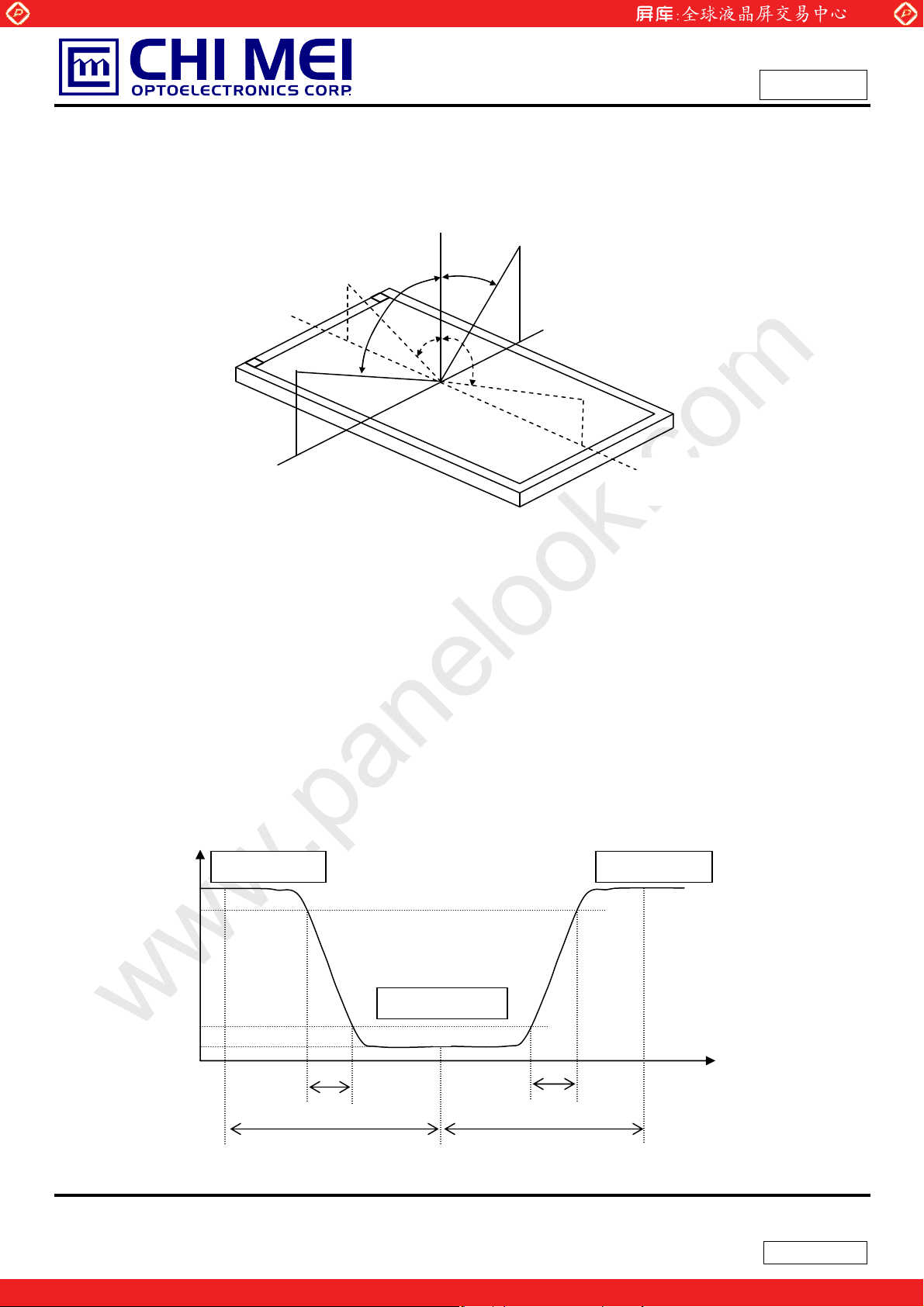
Note (1) Definition of Viewing Angle (θx, θy):
www.panelook.com
Issued Date :Feb, 17, 2009
Model No.: N156O6-L04
Tentative
Normal
θx = θy = 0º
θy- θy+
θX- = 90º
6 o’clock
θ
y- = 90º
x-
y-
Note (2) Definition of Contrast Ratio (CR):
The contrast ratio can be calculated by the following expression.
Contrast Ratio (CR) = L63 / L0
L63: Luminance of gray level 63
L 0: Luminance of gray level 0
CR = CR (1)
CR (X) is corresponding to the Contrast Ratio of the point X at Figure in Note (6).
θx−
θx+
12 o’clock direction
y+
θ
y+ = 90º
x+
θX+ = 90º
Note (3) Definition of Response Time (T
100%
90%
Optical
Response
10%
0%
T
66.67 ms
, TF):
R
Time
T
R
F
66
21 / 28
Version 0.0
One step solution for LCD / PDP / OLED panel application: Datasheet, inventory and accessory!
www.panelook.com
Page 22
Global LCD Panel Exchange Center
500
www.panelook.com
Issued Date :Feb, 17, 2009
Model No.: N156O6-L04
Tentative
Note (4) Definition of Average Luminance of White (L
Measure the luminance of gray level 63 at 5 points
L
= [L (1)+ L (2)+ L (3)+ L (4)+ L (5)] / 5
AVE
L (x) is corresponding to the luminance of the point X at Figure in Note (6)
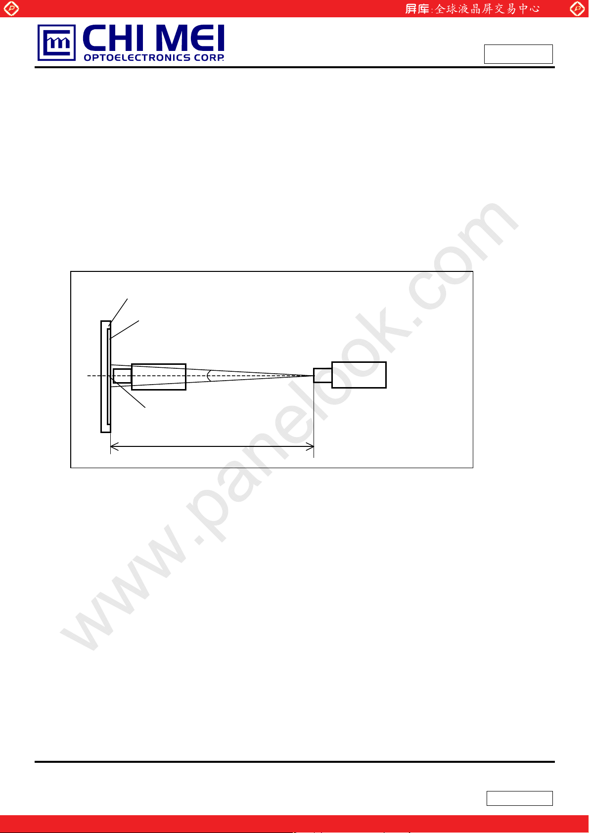
Note (5) Measurement Setup:
The LCD module should be stabilized at given temperature for 20 minutes to avoid abrupt
temperature change during measuring. In order to stabilize the luminance, the measurement
should be executed after lighting Backlight for 20 minutes in a windless room.
ʳ
LCD Module
LCD Panel
USB2000
AVE
):
CS-1000T
Center of the Screen
mm
Light Shield Room
(Ambient Luminance < 2 lux)
22 / 28
One step solution for LCD / PDP / OLED panel application: Datasheet, inventory and accessory!
Version 0.0
www.panelook.com
Page 23
Global LCD Panel Exchange Center
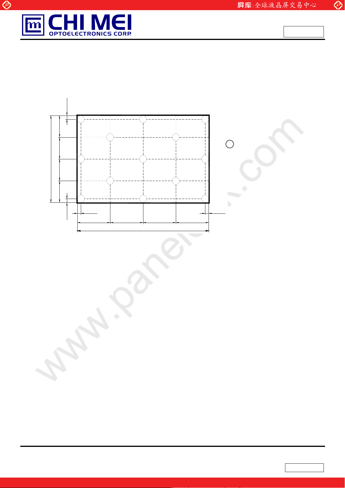
Note (6) Definition of White Variation (δW):
Measure the luminance of gray level 63 at 5 points
δW
= Minimum [L (1)+ L (2)+ L (3)+ L (4)+ L (5)] / Maximum [L (1)+ L (2)+ L (3)+ L (4)+ L (5)]
5p
˄˃
www.panelook.com
Issued Date :Feb, 17, 2009
Model No.: N156O6-L04
Tentative
ˉ
˛˂ˇ
˅
˄˃
ˌ
ˇˈ
˄˄
˄˃ ˄˃
˪˂ˇ ˪˂ˇ ˪˂ˇ ˪˂ˇ
˛
˛˂ˇ ˛˂ˇ ˛˂ˇ
ˊ
ˆ
˄
˄˅
˪
ˋ
X
: Test Point
˄˃
˄ˆ
X=1 to 13
Active area
23 / 28
One step solution for LCD / PDP / OLED panel application: Datasheet, inventory and accessory!
Version 0.0
www.panelook.com
Page 24
Global LCD Panel Exchange Center
9. PRECAUTIONS
9.1 HANDLING PRECAUTIONS
(1) The module should be assembled into the system firmly by using every mounting hole. Be careful not
to twist or bend the module.
(2) While assembling or installing modules, it can only be in the clean area. The dust and oil may cause
electrical short or damage the polarizer.
(3) Use fingerstalls or soft gloves in order to keep display clean during the incoming inspection and
assembly process.
(4) Do not press or scratch the surface harder than a HB pencil lead on the panel because the polarizer is
very soft and easily scratched.
(5) If the surface of the polarizer is dirty, please clean it by some absorbent cotton or soft cloth. Do not use
Ketone type materials (ex. Acetone), Ethyl alcohol, Toluene, Ethyl acid or Methyl chloride. It might
www.panelook.com
Issued Date :Feb, 17, 2009
Model No.: N156O6-L04
Tentative
permanently damage the polarizer due to chemical reaction.
(6) Wipe off water droplets or oil immediately. Staining and discoloration may occur if they left on panel for
a long time.
(7) If the liquid crystal material leaks from the panel, it should be kept away from the eyes or mouth. In
case of contacting with hands, legs or clothes, it must be washed away thoroughly with soap.
(8) Protect the module from static electricity, it may cause damage to the C-MOS Gate Array IC.
(9) Do not disassemble the module.
(10) Do not pull or fold the lamp wire.
(11) Pins of I/F connector should not be touched directly with bare hands.
9.2 STORAGE PRECAUTIONS
(1) High temperature or humidity may reduce the performance of module. Please store LCD module within
the specified storage conditions.
(2) It is dangerous that moisture come into or contacted the LCD module, because the moisture may
damage LCD module when it is operating.
(3) It may reduce the display quality if the ambient temperature is lower than 10 ºC. For example, the
response time will become slowly, and the starting voltage of lamp will be higher than the room
temperature.
9.3 OPERATION PRECAUTIONS
(1) Do not pull the I/F connector in or out while the module is operating.
(2) Always follow the correct power on/off sequence when LCD module is connecting and operating. This
can prevent the CMOS LSI chips from damage during latch-up.
(3) The startup voltage of Backlight is approximately 1000 Volts. It may cause electrical shock while
assembling with converter. Do not disassemble the module or insert anything into the Backlight unit.
24 / 28
One step solution for LCD / PDP / OLED panel application: Datasheet, inventory and accessory!
Version 0.0
www.panelook.com
Page 25
Global LCD Panel Exchange Center
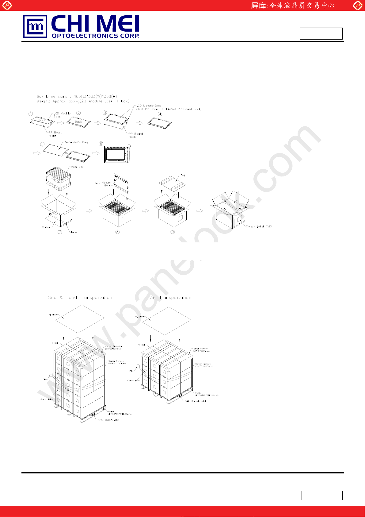
10. PACKING
10.1 CARTON
www.panelook.com
Issued Date :Feb, 17, 2009
Model No.: N156O6-L04
Tentative
10.2 PALLET
Figure. 10-1 Packing method
Figure. 10-2 Packing method
25 / 28
One step solution for LCD / PDP / OLED panel application: Datasheet, inventory and accessory!
Version 0.0
www.panelook.com
Page 26
Global LCD Panel Exchange Center
11.EFINITION OF LABELS
11.1 CMO MODULE LABEL
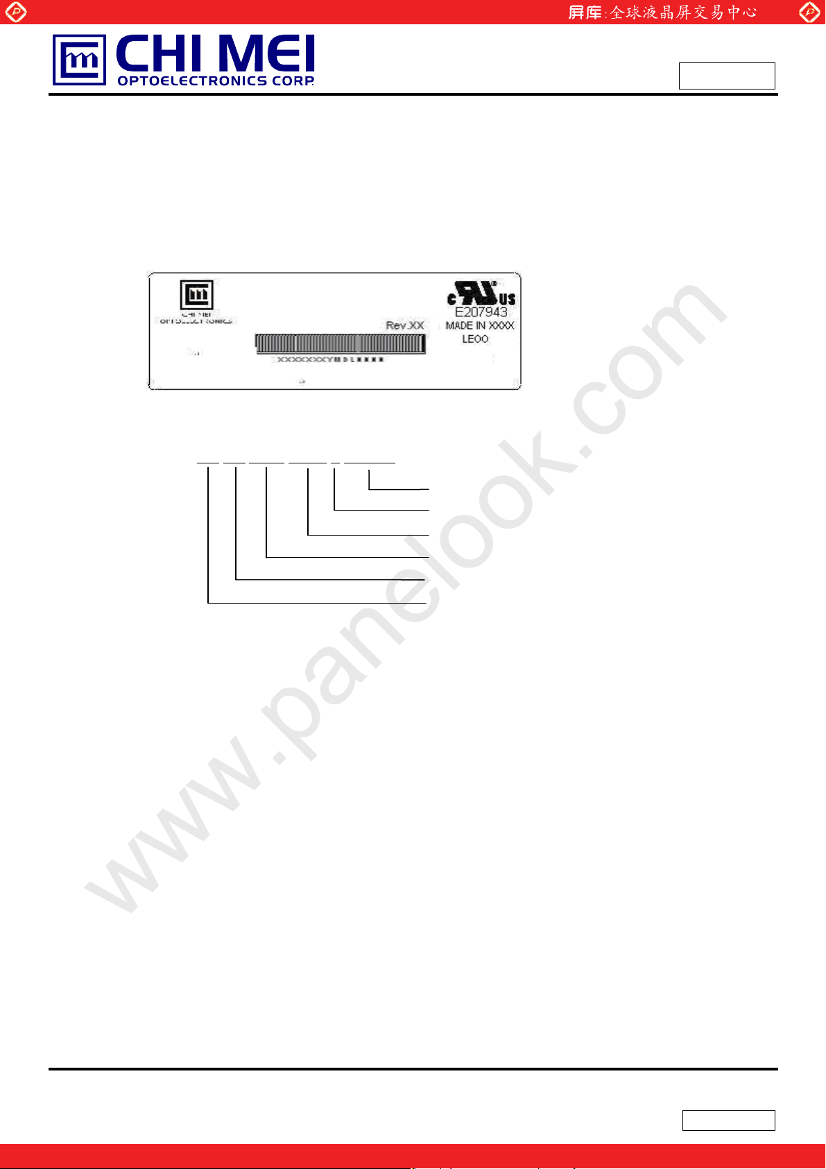
The barcode nameplate is pasted on each module as illustration, and its definitions are as following
explanation.
(a) Model Name: N156O6 - L04
www.panelook.com
Issued Date :Feb, 17, 2009
Model No.: N156O6-L04
Tentative
-
(b) Revision: Rev. XX, for example: A1, …, C1, C2 …etc.
(c) Serial ID: X X
(d) Production Location: MADE IN XXXX. XXXX stands for production location.
(e) UL/CB logo: “LEOO” especially stands for panel manufactured by CMO Ningbo satisfying UL/CB
requirement. “LEOO” is the CMO’s UL factory code for Ningbo factory.
Serial ID includes the information as below:
(a) Manufactured Date: Year: 1~9, for 2001~2009
(b) Revision Code: cover all the change
(c) Serial No.: Manufacturing sequence of product
X X X X X Y M D X N N N N
Month: 1~9, A~C, for Jan. ~ Dec.
Day: 1~9, A~Y, for 1
Serial No.
CMO Internal Use
Year, Month, Date
CMO Internal Use
Revision
CMO Internal Use
st
to 31st, exclude I , O and U
26 / 28
One step solution for LCD / PDP / OLED panel application: Datasheet, inventory and accessory!
Version 0.0
www.panelook.com
Page 27
Global LCD Panel Exchange Center
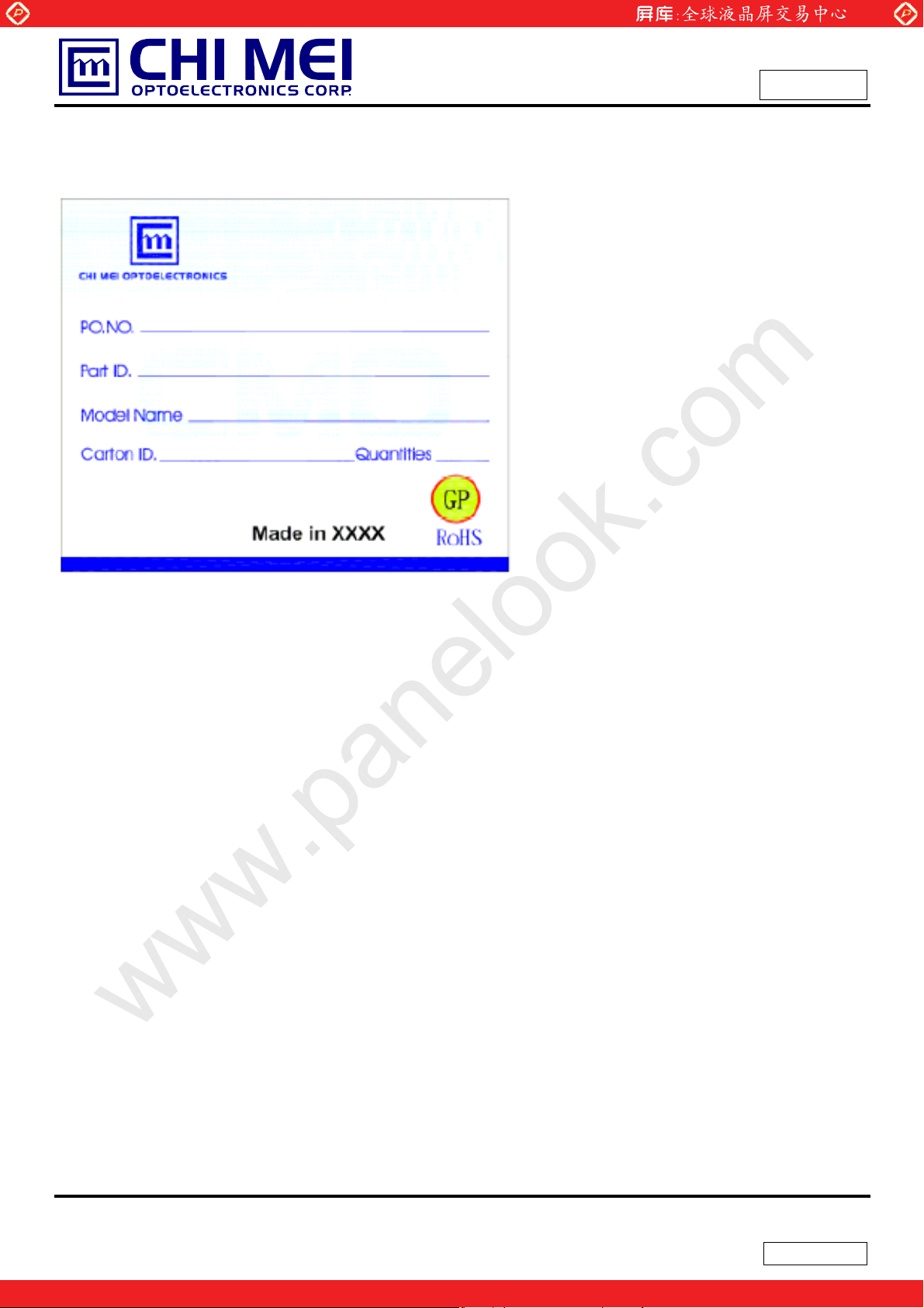
11.2 CARTON LABEL
www.panelook.com
Issued Date :Feb, 17, 2009
Model No.: N156O6-L04
Tentative
27 / 28
One step solution for LCD / PDP / OLED panel application: Datasheet, inventory and accessory!
Version 0.0
www.panelook.com
Page 28
Global LCD Panel Exchange Center
www.panelook.com
One step solution for LCD / PDP / OLED panel application: Datasheet, inventory and accessory!
www.panelook.com
 Loading...