

Page 1
Global LCD Panel Exchange Center
www.panelook.com
Global LCD Panel Exchange Center
www.panelook.com
Page 2
Global LCD Panel Exchange Center
www.panelook.com
Issued Date: Aug. 25. 2004
Model No.: N141XB -L04
Approval
- CONTENTS -
REVISION HISTORY
1. GENERAL DESCRIPTION
1.1 OVERVIEW
1.2 FEATURES
1.3 APPLICATION
1.4 GENERAL SPECIFICATIONS
1.5 MECHANICAL SPECIFICATIONS
2. ABSOLUTE MAXIMUM RATINGS
2.1 ABSOLUTE RATINGS OF ENVIRONMENT
2.2 ELECTRICAL ABSOLUTE RATINGS
2.2.1 TFT LCD MODULE
2.2.2 BACKLIGHT UNIT
3. ELECTRICAL CHARACTERISTICS
3.1 TFT LCD MODULE
3.2 BACKLIGHT UNIT
4. BLOCK DIAGRAM
4.1 TFT LCD MODULE
4.2 BACKLIGHT UNIT
5. INPUT TERMINAL PIN ASSIGNMENT
5.1 TFT LCD MODULE
5.2 BACKLIGHT UNIT
5.3 TIMING DIAGRAM OF LVDS INPUT SIGNAL
5.4 COLOR DATA INPUT ASSIGNMENT
6. INTERFACE TIMING
6.1 INPUT SIGNAL TIMING SPECIFICATIONS
6.2 POWER ON/OFF SEQUENCE
7. OPTICAL CHARACTERISTICS
7.1 TEST CONDITIONS
7.2 OPTICAL SPECIFICATIONS
8. PRECAUTIONS
8.1 HANDLING PRECAUTIONS
8.2 STORAGE PRECAUTIONS
8.3 OPERATION PRECAUTIONS
9. PACKING ------------------------------------------------------- 22
9.1 CARTON
9.2 PALLET
10. DEFINITION OF LABELS
10.1 CMO MODULE LABEL
10.2 CARTON LABEL
------------------------------------------------------- 3
------------------------------------------------------- 4
------------------------------------------------------- 5
------------------------------------------------------- 7
------------------------------------------------------- 11
------------------------------------------------------- 12
------------------------------------------------------- 15
------------------------------------------------------- 17
------------------------------------------------------- 21
------------------------------------------------------- 23
11. NATIOANL TEST LAB REQUIREMENT ------------------------------------------------------- 24
2 / 24
One step solution for LCD / PDP / OLED panel application: Datasheet, inventory and accessory!
Version 3.2
www.panelook.com
Page 3
Global LCD Panel Exchange Center
www.panelook.com
Issued Date: Aug. 25. 2004
Model No.: N141XB -L04
Approval
Version Date
Ver 0.0
Ver 1.0
Ver 2.0
Ver 3.0
Ver 3.1
Ver 3.2
Feb. 27. ‘04
Apr. 01. ‘04
Jul. 19. ‘04
Jul. 20. ‘04
Aug. 16. ‘04
Aug. 25. ‘04
Page
(New)
All
All
5
6
17
20
24
last
All
16
17
23
last
15
16
last
REVISION HISTORY
Section Description
Tentative specification first issued.
All
Preliminary specification first issued.
All
2.1
2.2
7.2
Outline
6.3
7.2
Outline
6.1
6.3
Outline
Modify table 2.1 and Note (3)
Add 2.2 Image Sticking
Modify the Specification of White Variation from Max/Min to Min/Max
Add White Variation of 13 points spec
Add Gamma Corrected Gray Scale Spec
Note (7) Modify the Definition of White Variation
Add National Test Lab Requirement
11
Update Outline Drawing - Add two Sponges
Issue Approval Specification for IBM/PCD
All
Modify the Min. Specification of t1 from 470us to 100us
Modify the Typ. Specification of Color Chromaticity Ry
from 0.345 to 0.335
Modify the Definition of Label
10
Modify Outline Drawing (S/N Label change)
Modify Min/Max value of vertical addressing time and horizontal
addressing time to blank
Minimum value of t4 change from 500 msec to 100 msec
Minimum value of t6 change from 200 msec to 0 msec
Add thickness spec of the sponges on rear surface
3 / 24
One step solution for LCD / PDP / OLED panel application: Datasheet, inventory and accessory!
Version 3.2
www.panelook.com
Page 4
Global LCD Panel Exchange Center
1. GENERAL DESCRIPTION
1.1 OVERVIEW
N141XB -L04 is a 14.1” TFT Liquid Crystal Display module with single CCFL Backlight unit and 30 pins
LVDS interface. This module supports 1024 x 768 XGA mode and can display 262,144 colors. The optimum
viewing angle is at 6 o’clock direction. The inverter module for Backlight is not built in.
1.2 FEATURES
- Thin and light weight
- XGA (1024 x 768 pixels) resolution
- DE (Data Enable) only mode
- 3.3V LVDS (Low Voltage Differential Signaling) interface with 1 pixel/clock
- SPWG (Standard Panel Working Group) Style B compatible
www.panelook.com
Issued Date: Aug. 25. 2004
Model No.: N141XB -L04
Approval
1.3 APPLICATION
- TFT LCD Notebook
1.4 GENERAL SPECIFICATI0NS
Item Specification Unit Note
Active Area 285.7 (H) x 214.3 (V) (14.1” diagonal) mm
Bezel Opening Area 288.9 (H) x 217.5 (V) mm
Driver Element a-si TFT active matrix - Pixel Number 1024 x R.G.B. x 768 pixel Pixel Pitch 0.279 (H) x 0.279 (V) mm Pixel Arrangement RGB vertical stripe - Display Colors 262,144 color Transmissive Mode Normally white - -
Surface Treatment
Hard coating (3H),
Anti-glare (Haze 40), Low-Reflection(less 3%)
- -
1.5 MECHANICAL SPECIFICATIONS
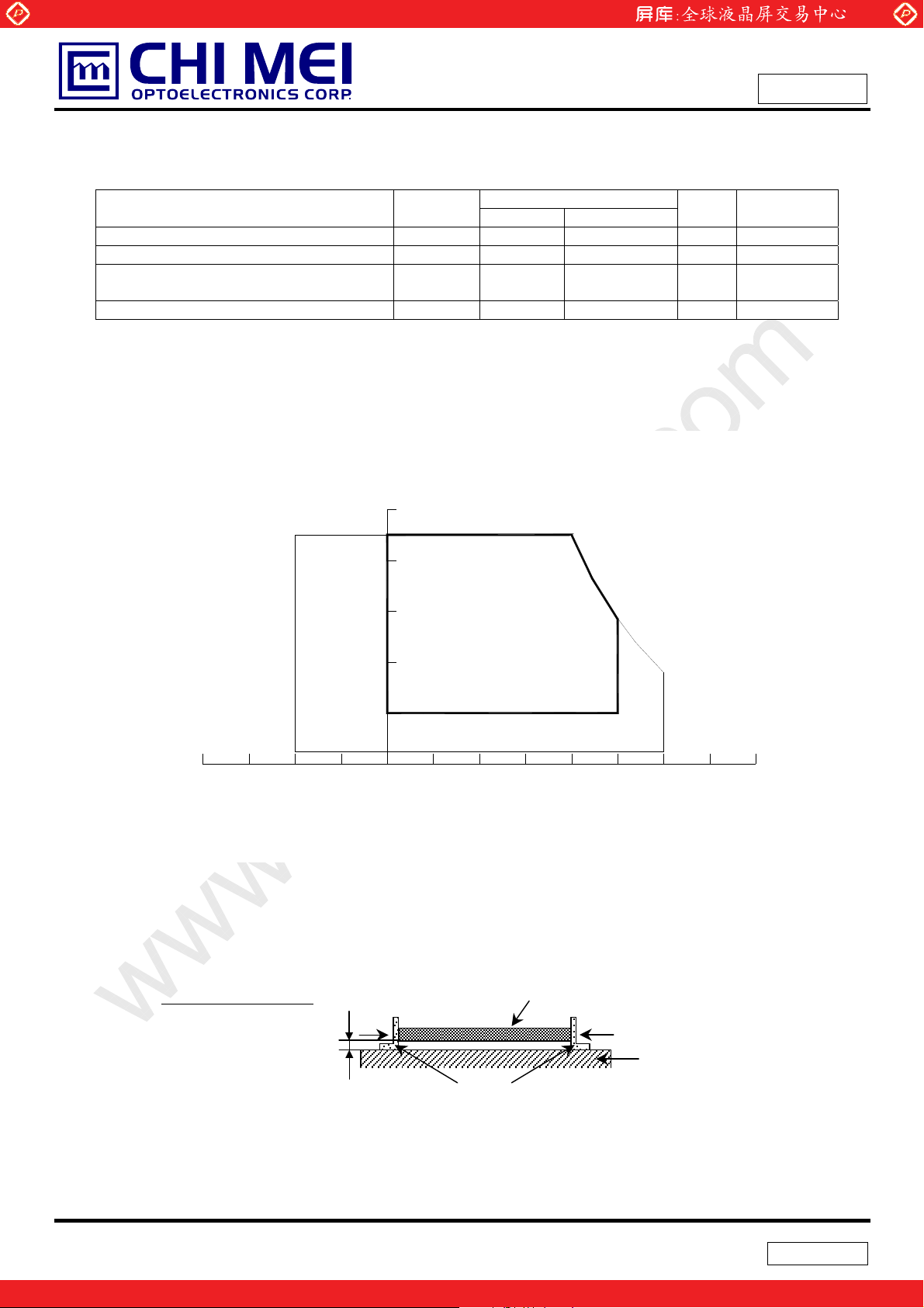
Item Min. Typ. Max. Unit Note
Horizontal(H) 298.5 299.0 299.5 mm
Module Size
I/F connector mounting position The mounting inclination of the connector makes the screen
Note (1) Please refer to the attached drawings for more information of front and back outline dimensions.
Vertical(V) 227.5 228.0 228.5 mm
Depth(D) - 5.2 5.5 mm
Weight - 420 430 g -
center within ±0.5mm as the horizontal.
(1)
(1)
(2)
(2) Connector mounting position
+/- 0.5mm
4 / 24
One step solution for LCD / PDP / OLED panel application: Datasheet, inventory and accessory!
Version 3.2
www.panelook.com
Page 5
Global LCD Panel Exchange Center
A
2. ABSOLUTE MAXIMUM RATINGS
2.1 ABSOLUTE RATINGS OF ENVIRONMENT
Item Symbol
Storage Temperature TST -20 +60 ºC (1)
Operating Ambient Temperature TOP 0 +50 ºC (1), (2)
Shock (Non-Operating) S
Vibration (Non-Operating) V
Note (1) Temperature and relative humidity range is shown in the figure below.
www.panelook.com
Min. Max.
-
NOP
- 1.5 10-200 G Hz (4), (5)
NOP
Value
50 18
220 2
Issued Date: Aug. 25. 2004
Model No.: N141XB -L04
Approval
Unit Note
G ms
G ms
(3), (4), (5)
(a) 90 %RH Max. (Ta
(b) Wet-bulb temperature should be 39 ºC Max. (Ta > 40 ºC).
(c) No condensation .
40 ºC).
Relative Humidity (%RH)
100
90
80
60
Operating Range
40
20
Storage Range
5
Temperature (ºC)
8060 -20 40020-40
Note (2) The temperature of panel surface should be 0 ºC Min. and 50 ºC Max.
Note (3) Condition for 50G 18ms is Rectangle Wave. Condition for 220G 2ms is Half Sine Wave.
Note (4) 10 ~ 200 Hz, 0.5 Hr / Cycle, 1 cycles for each X, Y, Z. The fixing condition is shown as below:
Note (5) At testing Vibration and Shock, the fixture in holding the module has to be hard and rigid enough
t Room Temperature
Side Mount Fixing Screw
Gap=2mm
so that the module would not be twisted or bent by the fixture.
Bracket
LCD Module
Side Mount Fixing Screw
Stage
5 / 24
One step solution for LCD / PDP / OLED panel application: Datasheet, inventory and accessory!
Version 3.2
www.panelook.com
Page 6
Global LCD Panel Exchange Center
2.2 IMAGE STICKING
No image sticking appears to anywhere of the display area after 10 hours kept with static images, 25degC
(30degC with LCD Module stand alone)
2.3 ELECTRICAL ABSOLUTE RATINGS
2.3.1 TFT LCD MODULE
Item Symbol
Power Supply Voltage Vcc -0.3 +4.0 V
Logic Input Voltage VIN -0.3 Vcc+0.3 V
2.3.2 BACKLIGHT UNIT
Item Symbol
Lamp Voltage VL - 2.5K V
Lamp Current IL - 7.0 mA
Lamp Frequency FL - 80 KHz
Note (1) Permanent damage to the device may occur if maximum values are exceeded. Function operation
www.panelook.com
Value
Min. Max.
Value
Min. Max.
Unit Note
Unit Note
Issued Date: Aug. 25. 2004
Model No.: N141XB -L04
Approval
(1)
(1), (2), IL = (6.0) mA
RMS
RMS
(1), (2)
should be restricted to the conditions described under Normal Operating Conditions.
Note (2) Specified values are for lamp (Refer to Section 3.2 for further information).
6 / 24
One step solution for LCD / PDP / OLED panel application: Datasheet, inventory and accessory!
Version 3.2
www.panelook.com
Page 7
Global LCD Panel Exchange Center
www.panelook.com
Issued Date: Aug. 25. 2004
Model No.: N141XB -L04
3. ELECTRICAL CHARACTERISTICS
3.1 TFT LCD MODULE Ta = 25 ± 2 ºC
Parameter Symbol
Min. Typ. Max.
Power Supply Voltage Vcc 3.0 3.3 3.6 V Ripple Voltage VRP - - 100 mV Rush Current I
- - 1.5 A (2)
RUSH
White - 350 380 mA (3)a
Power Supply Current
Black - 400 480 mA (3)b
Vertical Stripe
lcc
- 400 480 mA (3)c
“H” Level VIH - - +100 mV - Differential Input Voltage for
LVDS Receiver Threshold
“L” Level V
-100 - - mV -
IL
Terminating Resistor RT - 100 - Ohm -
Note (1) The module should be always operated within above ranges.
Note (2) Measurement Conditions:
Value
Unit Note
Approval
+3.3V
R1
47K
Q1 2SK1475
FUSE
C3
1uF
Vcc
(LCD Module Input)
(High to Low)
(Control Signal)
SW
+12V
C1
1uF
VR1
R2
1K
47K
0.01uF
Q2
2SK1470
C2
Vcc rising time is 470us
+3.3V
0.9Vcc
0.1Vcc
GND
470us
7 / 24
One step solution for LCD / PDP / OLED panel application: Datasheet, inventory and accessory!
Version 3.2
www.panelook.com
Page 8
Global LCD Panel Exchange Center
Note (3) The specified power supply current is under the conditions at Vcc = 3.3 V, Ta = 25 ± 2 ºC, DC
www.panelook.com
Issued Date: Aug. 25. 2004
Model No.: N141XB -L04
Approval
Current and f
a. White Pattern
c. Vertical Stripe Pattern
= 60 Hz, whereas a power dissipation check pattern below is displayed.
v
b. Black Pattern
B
B
R
R
R
Active Area
R
B
B
B
R
R
G
G
G
G
G
G
B
B
B
Active Area
R
R
R R
Active Area
G
B
G
B
3.2 BACKLIGHT UNIT Ta = 25 ± 2 ºC
Parameter Symbol
Lamp Input Voltage VL 576 640 704 V
Lamp Current IL 2.0 6.0 6.5 mA
Lamp Turn On Voltage VS
Operating Frequency FL 50 - 80 KHz (3)
Power Consumption PL - 3.84 - W (4), IL = 6.0 mA
Lamp Life Time LBL 10,000 15,000 - Hrs (5)
Leakage Current IIN-I
Note (1) Lamp current is measured by utilizing a high frequency current meter as shown below:
LCD
Module
- - 1.0 mA (7)
OUT
HV (Pink)
LV (White)
Min. Typ. Max.
- - 1360 (25
- - 1450 (0
Value
1
2
Current Meter
Unit Note
o
C) V
o
C) V
I
RMS
RMS
(2)
RMS
(2)
RMS
= 6.0 mA
L
(1) , (8)
Inverter
A
Note (2) The voltage shown above should be applied to the lamp for more than 1 second after startup.
Otherwise the lamp may not be turned on.
8 / 24
One step solution for LCD / PDP / OLED panel application: Datasheet, inventory and accessory!
Version 3.2
www.panelook.com
Page 9

Global LCD Panel Exchange Center
Note (3) The lamp frequency may generate interference with horizontal synchronous frequency from the
display, and this may cause line flow on the display. In order to avoid interference, the lamp
frequency should be detached from the horizontal synchronous frequency and its harmonics as far
as possible.
www.panelook.com
Issued Date: Aug. 25. 2004
Model No.: N141XB -L04
Approval
Note (4) P
Note (5) The lifetime of lamp is defined as the time when it continues to operate under the conditions at Ta
Note (6) The waveform of the voltage output of inverter must be area-symmetric and the design of the
Note (7) The lamp leakage current is measured by the current difference between in and out. And the
= IL x VL
L
= 25
(a) When the brightness becomes
(b) When the effective ignition length becomes
inverter must have specifications for the modularized lamp. The performance of the Backlight,
such as lifetime or brightness, is greatly influenced by the characteristics of the DC-AC inverter for
the lamp. All the parameters of an inverter should be carefully designed to avoid generating too
much current leakage from high voltage output of the inverter. When designing or ordering the
inverter please make sure that a poor lighting caused by the mismatch of the Backlight and the
inverter (miss-lighting, flicker, etc.) never occurs. If the above situation is confirmed, the module
should be operated in the same manners when it is installed in your instrument.
measurement condition is as below:
o
± 2
C and IL = 2.0~6.5 mA
until one of the following events occurs:
RMS
50% of its original value.
80% of its original value. (Effective ignition length
is defined as an area that the brightness is less than 70% compared to the center point.)
FG
GND
Low
I
Low
Current Probe
I
Leak(RMS)
LCD Module
Inverter
= I
Lamp
High(RMS)
- I
Low(RMS)
High
Current Probe
I
High
9 / 24
One step solution for LCD / PDP / OLED panel application: Datasheet, inventory and accessory!
Version 3.2
www.panelook.com
Page 10

Global LCD Panel Exchange Center
Note (8) About operating current min 2.0mA , lamp maker has some advice as below
www.panelook.com
Issued Date: Aug. 25. 2004
Model No.: N141XB -L04
Approval
10 / 24
One step solution for LCD / PDP / OLED panel application: Datasheet, inventory and accessory!
Version 3.2
www.panelook.com
Page 11

Global LCD Panel Exchange Center
)
4. BLOCK DIAGRAM
4.1 TFT LCD MODULE
www.panelook.com
Issued Date: Aug. 25. 2004
Model No.: N141XB -L04
Approval
Rxin0(+/-)
Rxin1(+/-)
Rxin2(+/-)
CLK(+/-)
(JAE-FI- XB30SL-HF10)
Vcc
GND
VL
LAMP CONNECTOR
4.2 BACKLIGHT UNIT
INPUT CONNECTOR
(JST-BHSR-02VS-1)
TIMING CONTROLLER
DC/DC CONVERTER &
REFERENCE VOLTAGE
LVDS INPUT /
GENERATOR
SCAN DRIVER IC
TFT LCD PANEL
(1024x3x768)
DATA DRIVER IC
BACKLIGHT UNIT
1 HV (Pink)
2 LV (Black
11 / 24
One step solution for LCD / PDP / OLED panel application: Datasheet, inventory and accessory!
Version 3.2
www.panelook.com
Page 12

Global LCD Panel Exchange Center
5. INPUT TERMINAL PIN ASSIGNMENT
5.1 TFT LCD MODULE
Pin Symbol Description Polarity Remark
1 Vss Ground
2 Vcc Power Supply +3.3 V (typical)
3 Vcc Power Supply +3.3 V (typical)
4 NC Non-Connection
5 NC Non-Connection
6 NC Non-Connection
7 NC Non-Connection
8 Rxin0- LVDS Differential Data Input Negative
9 Rxin0+ LVDS Differential Data Input Positive
10 Vss Ground
11 Rxin1- LVDS Differential Data Input Negative
12 Rxin1+ LVDS Differential Data Input Positive
13 Vss Ground
14 Rxin2- LVDS Differential Data Input Negative
15 Rxin2+ LVDS Differential Data Input Positive
16 Vss Ground
17 CLK- LVDS Clock Data Input Negative
18 CLK+ LVDS Clock Data Input Positive
19 Vss Ground
20 NC Non-Connection
21 NC Non-Connection
22 Vss Ground
23 NC Non-Connection
24 NC Non-Connection
25 Vss Ground
26 NC Non-Connection
27 NC Non-Connection
28 Vss Ground
29 NC Non-Connection
30 NC Non-Connection
Note (1) The first pixel is even.
www.panelook.com
Issued Date: Aug. 25. 2004
Model No.: N141XB -L04
Approval
R0~R5,G0
-
G1~G5,B0,B1
-
B2~B5,DE,Hsync,Vsync
LVDS Level Clock
Note (2) Connector Part No.: JAE-FI-XB30SL-HF10 or equivalent
Note (3) User’s connector Part No: JAE-FI-X30C2L or equivalent
5.2 BACKLIGHT UNIT
Pin Symbol Description Color
1 HV High Voltage Pink
2 LV Ground Black
Note (1) Connector Part No.: JST-BHSR-02VS-1 or equivalent
Note (2) User’s connector Part No.: JST-SM02B-BHSS-1-TB or equivalent
12 / 24
One step solution for LCD / PDP / OLED panel application: Datasheet, inventory and accessory!
Version 3.2
www.panelook.com
Page 13

Global LCD Panel Exchange Center
5.3 TIMING DIAGRAM OF LVDS INPUT SIGNAL
CLK+
T/7
www.panelook.com
Issued Date: Aug. 25. 2004
Model No.: N141XB -L04
Approval
Rxin2
Rxin1
Rxin0
IN20 IN19 IN18 IN17 IN16 IN15 IN14
DE B5 B4 B3 B2 Vsync Hsync
IN13 IN12 IN11 IN10 IN9 IN8 IN7
B1 G4 G3 G2 G1 B0 G5
IN6 IN5 IN4 IN3 IN2 IN1 IN0
G0 R3 R2 R1 R0 R5 R4
Signal for 1 DCLK Cycle (T)
13 / 24
One step solution for LCD / PDP / OLED panel application: Datasheet, inventory and accessory!
Version 3.2
www.panelook.com
Page 14

Global LCD Panel Exchange Center
5.4 COLOR DATA INPUT ASSIGNMENT
The brightness of each primary color (red, green and blue) is based on the 6-bit gray scale data input for
the color. The higher the binary input the brighter the color. The table below provides the assignment of
color versus data input.
Color
R5 R4 R3 R2 R1 R0 G5 G4 G3 G2 G1 G0 B5 B4 B3 B2 B1 B0
Black
Red
Green
Basic
Colors
Gray
Scale
Of
Red
Gray
Scale
Of
Green
Gray
Scale
Of
Blue
Note (1) 0: Low Level Voltage, 1: High Level Voltage
Blue
Cyan
Magenta
Yellow
White
Red(0)/Dark
Red(1)
Red(2)
:
:
Red(61)
Red(62)
Red(63)
Green(0)/Dark
Green(1)
Green(2)
:
:
Green(61)
Green(62)
Green(63)
Blue(0)/Dark
Blue(1)
Blue(2)
:
:
Blue(61)
Blue(62)
Blue(63)
0
0
1
1
0
0
0
0
0
0
1
1
1
1
1
1
0
0
0
0
0
0
:
:
:
:
1
1
1
1
1
1
0
0
0
0
0
0
:
:
:
:
0
0
0
0
0
0
0
0
0
0
0
0
:
:
:
:
0
0
0
0
0
0
www.panelook.com
Issued Date: Aug. 25. 2004
Model No.: N141XB -L04
Approval
Data Signal
Red Green Blue
0
0
0
0
0
0
0
0
0
0
0
0
0
0
0
0
1
1
1
1
0
0
0
0
0
0
0
0
0
0
0
0
0
0
0
0
1
1
1
1
1
1
0
0
0
0
0
0
0
0
0
0
0
0
0
0
0
0
1
1
1
1
1
1
0
0
0
0
1
1
1
1
1
1
1
1
1
1
1
1
1
1
1
1
0
0
0
0
0
0
1
1
1
1
1
1
1
1
1
1
1
1
1
1
1
1
0
0
0
0
0
0
1
1
1
1
1
1
1
1
1
1
1
1
1
1
1
1
0
0
0
0
0
0
0
0
0
0
0
0
0
0
0
0
0
0
0
1
0
0
0
0
0
0
0
0
0
0
0
0
0
0
1
0
0
0
0
0
0
0
0
0
0
0
0
0
:
:
:
:
:
:
:
:
:
:
:
:
:
:
:
:
:
:
:
:
:
:
:
:
:
:
:
:
:
:
:
:
1
1
0
1
0
0
0
0
0
0
0
0
0
0
0
0
1
1
1
0
0
0
0
0
0
0
0
0
0
0
0
0
1
1
1
1
0
0
0
0
0
0
0
0
0
0
0
0
0
0
0
0
0
0
0
0
0
0
0
0
0
0
0
0
0
0
0
0
0
0
0
0
0
1
0
0
0
0
0
0
0
0
0
0
0
0
0
0
1
0
0
0
0
0
0
0
:
:
:
:
:
:
:
:
:
:
:
:
:
:
:
:
:
:
:
:
:
:
:
:
:
:
:
:
:
:
:
:
0
0
0
0
1
1
1
1
0
1
0
0
0
0
0
0
0
0
0
0
1
1
1
1
1
0
0
0
0
0
0
0
0
0
0
0
1
1
1
1
1
1
0
0
0
0
0
0
0
0
0
0
0
0
0
0
0
0
0
0
0
0
0
0
0
0
0
0
0
0
0
0
0
0
0
0
0
0
0
1
0
0
0
0
0
0
0
0
0
0
0
0
0
0
1
0
:
:
:
:
:
:
:
:
:
:
:
:
:
:
:
:
:
:
:
:
:
:
:
:
:
:
:
:
:
:
:
:
0
0
0
0
0
0
0
0
0
0
1
1
1
1
0
1
0
0
0
0
0
0
0
0
0
0
1
1
1
1
1
0
0
0
0
0
0
0
0
0
0
0
1
1
1
1
1
1
14 / 24
One step solution for LCD / PDP / OLED panel application: Datasheet, inventory and accessory!
Version 3.2
www.panelook.com
Page 15

Global LCD Panel Exchange Center
6. INTERFACE TIMING
6.1 INPUT SIGNAL TIMING SPECIFICATIONS
The input signal timing specifications are shown as the following table and timing diagram.
Signal Item Symbol Min. Typ. Max. Unit Note
DCLK Frequency 1/Tc 50 65 68 MHz -
Vertical Total Time TV 771 806 850 TH -
DE
Vertical Addressing Time TVD - 768 - TH -
Horizontal Total Time TH 1200 1344 1500 Tc -
Horizontal Addressing Time THD - 1024 - Tc -
www.panelook.com
Issued Date: Aug. 25. 2004
Model No.: N141XB -L04
Approval
INPUT SIGNAL TIMING DIAGRAM
DE
DCLK
T
DE
DATA
TVD
C
v
T
T
H
HD
T
6.2 Self-Protection Mode
There are two kind of conditions that timing controller will go to the self-protection mode.
(1) Clock Stop Detection
If dot clock stops still about 100ms, timing controller goes into the self-protection mode.
(2) DE Signal Detection
If the time of DE as low is longer than 1 frame, timing controller goes into the self-protection mode.
Once the self-protection mode is active, the panel will display black pattern.
15 / 24
One step solution for LCD / PDP / OLED panel application: Datasheet, inventory and accessory!
Version 3.2
www.panelook.com
Page 16

Global LCD Panel Exchange Center
6.3 POWER ON/OFF SEQUENCE
Power On
www.panelook.com
Power Off
Issued Date: Aug. 25. 2004
Model No.: N141XB -L04
Approval
Restart
Power Supply
for LCD, Vcc
- Interface Signal
(LVDS Signal of
Transmitter), V
- Power for Lamp
Timing Specifications:
100us
0 < t2
0 < t3
0V
0V
I
t1 10 msec
50 msec
50 msec
t4
> 100 msec
t5
> 200 msec
10%
90%
t1
90%
Valid Data
t6 t5
ONOFF OFF
t4
10%
t3 t2
10%
t6
> 0 msec
Note (1) Please avoid floating state of interface signal at invalid period.
Note (2) When the interface signal is invalid, be sure to pull down the power supply of LCD Vcc to 0 V.
Note (3) The Backlight inverter power must be turned on after the power supply for the logic and the
interface signal is valid. The Backlight inverter power must be turned off before the power supply
for the logic and the interface signal is invalid.
16 / 24
One step solution for LCD / PDP / OLED panel application: Datasheet, inventory and accessory!
Version 3.2
www.panelook.com
Page 17

Global LCD Panel Exchange Center
7. OPTICAL CHARACTERISTICS
7.1 TEST CONDITIONS
Item Symbol Value Unit
Ambient Temperature Ta 25r2
Ambient Humidity Ha 50r10 %RH
Supply Voltage VCC 3.3 V
Input Signal According to typical value in "3. ELECTRICAL CHARACTERISTICS"
Inverter Current IL
Inverter Driving Frequency FL
Inverter Sumida-H05-4783B
The measurement methods of optical characteristics are shown in Section 7.2. The following items
should be measured under the test conditions described in Section 7.1 and stable environment shown in
Note (6).
www.panelook.com
6.0
55
Issued Date: Aug. 25. 2004
Model No.: N141XB -L04
Approval
o
C
mA
KHz
7.2 OPTICAL SPECIFICATIONS
Item Symbol Condition Min. Typ. Max. Unit Note
Contrast Ratio CR 150 250 - - (2), (6)
Response Time
Average Luminance of White L
TR
T
F
130 150 - cd/m2(4), (6)
AVE
White Variation of 5 Points GW5p 80 - - % (6), (7)
White Variation of 13 Points GW
65 - - & (6), (7)
13p
Cross Talk CT - - 4.0 % (5), (6)
T
=0q, TY =0q
x
Viewing Normal Angle
Color
Chromaticity
Red
Green
Blue
White
Rx 0.570 Ry 0.335 Gx 0.325 Gy 0.570 -
Bx 0.150 -
By
Wx
Wy
Color Gamut C.G%
Horizontal
Viewing Angle
Vertica l
Tx+ 40 45 -
- 40 45 -
T
x
TY+ 10 15 -
T
-
Y
CRt10
L0
L7
L15
Gamma Corrected Gray
Scale
L23
L31
L39
T
=0q, TY =0q
x
Viewing Normal Angle
L47
L55
L63
- 6 10 ms
- 17 25 ms
Typ.
-0.03
Typ.
+0.03
0.125
0.285 0.313 0.341
0.309 0.329 0.349
45 - % (8)
Deg. (1), (6)
25 35 -
0
2
5
10
-
22
- % 6bit
36
53
75
100
(3)
(1), (6)
-
-
-
17 / 24
One step solution for LCD / PDP / OLED panel application: Datasheet, inventory and accessory!
Version 3.2
www.panelook.com
Page 18

Global LCD Panel Exchange Center
Note (1) Definition of Viewing Angle (Tx, Ty):
www.panelook.com
Issued Date: Aug. 25. 2004
Model No.: N141XB -L04
Approval
TX- = 90º
x-
6 o’clock
T
y- = 90º
y-
Note (2) Definition of Contrast Ratio (CR):
The contrast ratio can be calculated by the following expression.
Normal
Tx = Ty = 0º
Ty- Ty
Tx-
Tx+
y+
12 o’clock direction
T
y+ = 90º
x+
TX+ = 90º
Contrast Ratio (CR) = L63 / L0
L63: Luminance of gray level 63
L 0: Luminance of gray level 0
CR = CR (5)
CR (X) is corresponding to the Contrast Ratio of the point X at Figure in Note (7).
Note (3) Definition of Response Time (T
100%
90%
Optical
Response
10%
0%
R
T
R
, TF):
Time
T
F
18 / 24
One step solution for LCD / PDP / OLED panel application: Datasheet, inventory and accessory!
Version 3.2
www.panelook.com
Page 19

Global LCD Panel Exchange Center
A
A
www.panelook.com
Issued Date: Aug. 25. 2004
Model No.: N141XB -L04
Approval
Note (4) Definition of Average Luminance of White (L
Measure the luminance of gray level 63 at 5 points
L
= [L (1)+ L (2)+ L (3)+ L (4)+ L (5)] / 5
AVE
L (x) is corresponding to the luminance of the point X at Figure in Note (7).
Note (5) Definition of Cross Talk (CT):
CT = | Y
– YA | / YA u 100 (%)
B
Where:
Y
= Luminance of measured location without gray level 0 pattern (cd/m2)
A
Y
= Luminance of measured location with gray level 0 pattern (cd/m2)
B
(0, 0)
ctive Area
Y
(D/8,W/2)
A, L
Gray 32
Y
(D/2,7W/8)
A, D
(D,W)
Y
(D/2,W/8)
A, U
Y
(7D/8,W/2)
A, R
AVE
):
(D/4,W/4)
Y
(D/8,W/2)
B, L
Y
(D/2,7W/8)
B, D
(0, 0)
ctive Area
Gray 0
Gray 32
Y
B, U
Y
B, R
(3D/4,3W/4)
(D,W)
(D/2,W/8)
(7D/8,W/2)
Note (6) Measurement Setup:
The LCD module should be stabilized at given temperature for 20 minutes to avoid abrupt
temperature change during measuring. In order to stabilize the luminance, the measurement
should be executed after lighting Backlight for 20 minutes in a windless room.
LCD Module
LCD Panel
Center of the Screen
500 mm
Photometer
(TOPCON BM-5A)
Field of View = 2º
Light Shield Room
(Ambient Luminance < 2 lux)
19 / 24
One step solution for LCD / PDP / OLED panel application: Datasheet, inventory and accessory!
Version 3.2
www.panelook.com
Page 20

Global LCD Panel Exchange Center
Note (7) Definition of White Variation (GW):
Measure the luminance of gray level 63 at 13 points
GW
= Minimum [L (1), L (2), L (3), L (4), L (5)] / Maximum [L (1), L (2), L (3), L (4), L (5)]
5p
GW
= Minimum [L (1) ~ L (13)] / Maximum [L (1) ~ L (13)]
13p
www.panelook.com
Issued Date: Aug. 25. 2004
Model No.: N141XB -L04
Approval
Horizontal Line
10mm
D/4 D/2 3D/4
10mm
6
W/4
W
W/2
9
23
Vertical Line
3W/4
10mm
4
11 12 13
Active Area
Note (8) Definition of color gamut (C.G%):
C.G%= 'R G B /'R
R
R, G, B
'R
, G0, B0 : color coordinates of red, green, and blue defined by NTSC, respectively.
0
: color coordinates of module on 63 gray levels of red, green, and blue, respectively.
0 G0 B0
: area of triangle defined by R0, G0, B0
0 G0 B0
,*100%
'R G B: area of triangle defined by R, G, B
D
10mm
10
8
X
: Test Point
X=1 to 13
7
1
5
˖˜˘ʳ˄ˌˆ˄
˃ˁˌ
˃ˁˋ
˃ˁˊ
˃ˁˉ
˃ˁˈ
˃ˁˇ
˃ˁˆ
˃ˁ˅
˃ˁ˄
˃
˃ ˃ˁ˅ ˃ˁˇ ˃ˁˉ ˃ˁˋ
G
0
G
R
0
R
B
B
0
20 / 24
One step solution for LCD / PDP / OLED panel application: Datasheet, inventory and accessory!
Version 3.2
www.panelook.com
Page 21

Global LCD Panel Exchange Center
8. PRECAUTIONS
8.1 HANDLING PRECAUTIONS
(1) The module should be assembled into the system firmly by using every mounting hole. Be careful not
to twist or bend the module.
(2) While assembling or installing modules, it can only be in the clean area. The dust and oil may cause
electrical short or damage the polarizer.
(3) Use fingerstalls or soft gloves in order to keep display clean during the incoming inspection and
assembly process.
(4) Do not press or scratch the surface harder than a HB pencil lead on the panel because the polarizer is
very soft and easily scratched.
(5) If the surface of the polarizer is dirty, please clean it by some absorbent cotton or soft cloth. Do not use
Ketone type materials (ex. Acetone), Ethyl alcohol, Toluene, Ethyl acid or Methyl chloride. It might
www.panelook.com
Issued Date: Aug. 25. 2004
Model No.: N141XB -L04
Approval
permanently damage the polarizer due to chemical reaction.
(6) Wipe off water droplets or oil immediately. Staining and discoloration may occur if they left on panel for
a long time.
(7) If the liquid crystal material leaks from the panel, it should be kept away from the eyes or mouth. In
case of contacting with hands, legs or clothes, it must be washed away thoroughly with soap.
(8) Protect the module from static electricity, it may cause damage to the C-MOS Gate Array IC.
(9) Do not disassemble the module.
(10) Do not pull or fold the lamp wire.
(11) Pins of I/F connector should not be touched directly with bare hands.
8.2 STORAGE PRECAUTIONS
(1) High temperature or humidity may reduce the performance of module. Please store LCD module within
the specified storage conditions.
(2) It is dangerous that moisture come into or contacted the LCD module, because the moisture may
damage LCD module when it is operating.
(3) It may reduce the display quality if the ambient temperature is lower than 10 ºC. For example, the
response time will become slowly, and the starting voltage of lamp will be higher than the room
temperature.
8.3 OPERATION PRECAUTIONS
(1) Do not pull the I/F connector in or out while the module is operating.
(2) Always follow the correct power on/off sequence when LCD module is connecting and operating. This
can prevent the CMOS LSI chips from damage during latch-up.
(3) The startup voltage of Backlight is approximately 1000 Volts. It may cause electrical shock while
assembling with inverter. Do not disassemble the module or insert anything into the Backlight unit.
21 / 24
One step solution for LCD / PDP / OLED panel application: Datasheet, inventory and accessory!
Version 3.2
www.panelook.com
Page 22

Global LCD Panel Exchange Center
9. PACKING
9.1 CARTON
www.panelook.com
Issued Date: Aug. 25. 2004
Model No.: N141XB -L04
Approval
9.2 PALLET
22 / 24
One step solution for LCD / PDP / OLED panel application: Datasheet, inventory and accessory!
Version 3.2
www.panelook.com
Page 23

Global LCD Panel Exchange Center
Y
www.panelook.com
Issued Date: Aug. 25. 2004
Model No.: N141XB -L04
Approval
10. DEFINITION OF LABELS
10.1 CMO MODULE LABEL
The barcode nameplate is pasted on each module as illustration, and its definitions are as following explanation.
ear/ Week
ZZZZ
E207943
%/1
11S92P6674Z1ZXXXXXXXXX N141X7 -L04 P/N: 92P6674 FRU: 92P6675
11S92P6730Z1Z9V5XXXXXX N141XB –L04 P/N: 92P6730 FRU: 92P6731
/#&'+ 06#+ 9#0
/%
10.2 CARTON LABEL
CMO Model Name
CMO Internal Use
N141XB –L04
XX pcs
XX/XX/XX
23 / 24
One step solution for LCD / PDP / OLED panel application: Datasheet, inventory and accessory!
Version 3.2
www.panelook.com
Page 24

Global LCD Panel Exchange Center
www.panelook.com
Issued Date: Aug. 25. 2004
Model No.: N141XB -L04
Approval
11. NATIONAL TEST LAB REQUIREMENT
The display module is authorized to Apply the UL Recognized Mark.
Conditions of Acceptability
Conditions of Acceptability - When installed on the end-product, consideration shall be given to the following;
1. This component has been judged on the basis of the required spacings in the Standard for Safety of
Information Technology Equipment, CSA/UL60950, which would cover the component itself if submitted for
Listing.
2. The unit is intended to be supplied by SELV and Limited Power Source. Also separated from electrical parts,
which may produce high temperature that could cause ignition by as least 13mm of air or by a solid barrier of
material of V-1 minimum.
3. The terminals and connectors are suitable for factory wiring only.
4. A suitable electrical enclosure shall be provided.
24 / 24
One step solution for LCD / PDP / OLED panel application: Datasheet, inventory and accessory!
Version 3.2
www.panelook.com
Page 25

Global LCD Panel Exchange Center
www.panelook.com
One step solution for LCD / PDP / OLED panel application: Datasheet, inventory and accessory!
www.panelook.com
 Loading...