

Page 1

Global LCD Panel Exchange Center
www.panelook.com
Global LCD Panel Exchange Center
www.panelook.com
Page 2
Global LCD Panel Exchange Center
www.panelook.com
CONTENTS
REVISION HISTORY
GENERAL DESCRIPTION
1. ABSOLUTE MAXIMUM RATINGS
1.1 ABSOLUTE RATING OF ENVIRONMENT
1.2 ELECTRICAL ABSOLUTE RATINGS
1.3 MECHANICAL RATINGS
1.4 THE OTHERS
2. ELECTRICAL SPECIFICATIONS
2.1 TFT LCD MODULE
2.2 BACKLIGHT UNIT
2.3 MATERIAL LIST CONCERNING EMI REGULATIONS
3. INTERFACE SPECIFICATIONS
3.1 THE PIN ASSIGNMENT OF LVDS INTERFACE CONNECTOR
3.2 INPUT SIGNAL TIMING SPECIFICATIONS
3.3 COLOR DATA INPUT ASSIGNMENT
3.4 POWER UP/DOWN SEQUENCE
4. OPTICAL SPECIFICATIONS
4.1 TEST CONDITIONS
4.2 OPTICAL SPECIFICATIONS
5. MECHNICAL DRAWING
6. PRECAUTION
6.1 ASSEMBLY AND HANDLING PRECAUTION
6.2 SAFTY PRECAUTION
7. PACKING
7.1 PACKING SPECIFICATIONS
7.2 PACKING METHOD
8. DEFINITION OF SHIPPING LABEL ON MODULE
Attached 1, Outline Drawing
Issued Date: Apr. 19, 2004
Model No. : N141XB-L02
Approval
2 / 26
One step solution for LCD / PDP / OLED panel application: Datasheet, inventory and accessory!
Version 3.1
www.panelook.com
Page 3
Global LCD Panel Exchange Center
REVISION HISTORY
Version Date
Ver 1.0
Ver 3.0
Ver 3.1
Feb. 10,’04
Mar. 30,’04
Apr. 19,’04
Page
(New)
All
9
11
12
15
4
7
9
12
15
17
18
Last
www.panelook.com
Issued Date: Apr. 19, 2004
Model No. : N141XB-L02
Approval
Section Description
All
2.2
3.1
3.4.1
1.3
2.1
3.1
3.4.1
4.2
Drawing
Preliminary Specification was first issued.
Startup Voltage 1760 Ш 1500 Vrms
Added Leak current
Added Note( 8 )
Pin 4~7 Non Connection
Added power off timing specifications t7
Modify Block Diagram
-
Modify Mechanical specification
Module Size Horizontal 299.0 r 0.3 mm , Vertical 228.0 r 0.3 mm
Added min value of depth and weight
Delete Note(4)
Update Power Supply Current Specifications
Revised Note(10) in page 11
Delete “Leakage Current”
Revised Pin 4~7
Delete “ or equivalent “ in Note(2) and Note(3)
Change t5 Њ200 msec to t5 Њ100 msec
Change t6 Њ200 msec to t6 Њ100 msec
Delete power off timing specifications t7
Average luminance of white(5 points) : 160 Typ Ш 170 Typ
Add Gamma Specification Min and Max Value
Modify outline dimension tolerance r 0.5 Ш r 0.3
Delete Active Area dimension tolerance r 0.2
3 / 26
One step solution for LCD / PDP / OLED panel application: Datasheet, inventory and accessory!
Version 3.1
www.panelook.com
Page 4
Global LCD Panel Exchange Center
ɡ
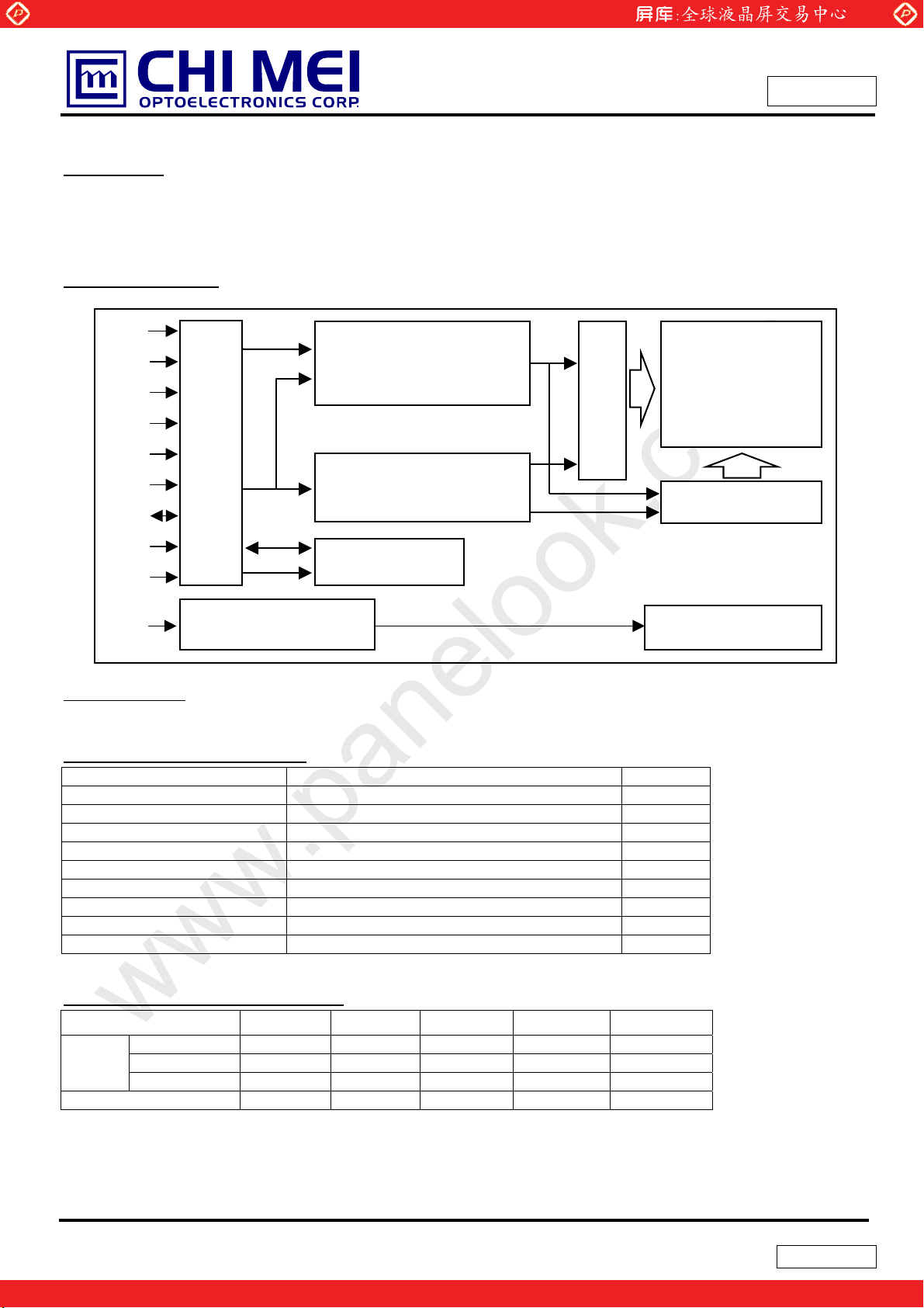
GENERAL DESCRIPTION
www.panelook.com
Issued Date: Apr. 19, 2004
Model No. : N141XB-L02
Approval
OVERVIEW
This is a 14.1” TFT Liquid Crystal Display module with single CCFL Backlight unit and 30 pins LVDS interface. This
module supports 1024 x 768 XGA mode and can display 262,144 colors. The optimum viewing angle is at 6 o’clock
direction. The inverter module for Backlight is not built in.
BLOCK DIAGRAM
Rxin0(+/-)
Rxin1(+/-)
Rxin2(+/-)
CLK(+/-)
Vcc
GND
Data
EDID
CLK
EDID
V
EDID
(JAE-FI- XB30SL-HF10)
INPUT CONNECTOR
LVDS INPUT /
TIMING CONTROLLER
DC/DC CONVERTER &
REFERENCE VOLTAGE
GENERATOR
EDID
EEPROM
SCAN DRIVER IC
TFT LCD PANEL
(1024x3x768)
DATA DRIVER IC
VL
LAMP CONNECTOR
(JST-BHTR-02VS-1)
BACKLIGHT UNIT
APPLICATION
-Note Book PC
GENERAL SPECIFICATI0NS
Item Specifications Unit
Screen Size 14.1 Diagonal inch
Bezel opening area 288.9 (H) x 217.5 (V) mm
Effective display area 285.7(W)x214.3(H) mm
Pixel number 1024 x R.G.Bx768 pixel
Pixel pitch 0.279(H)x0.279(V) mm
Pixel Arrangement R.G.B Vertical Stripe Display Color 6 bits, 262,144 color
Transmissive mode Normally white Surface treatments Hardness (3H), Anti-glare (Haze 25) -
MECHANICAL SPECIFICATIONS
ITEM MIN. TYP. MAX. Unit Note
Module
Size
Note 1: The maximum thickness of I/O connector area is 5.5mm.
Horizontal 298.7 299.0 299.3 mm Vertical 227.7 228.0 228.3 mm Depth 4.9 5.2 5.5 mm (1)
Weight 405 420 430 g -
4 / 26
One step solution for LCD / PDP / OLED panel application: Datasheet, inventory and accessory!
Version 3.1
www.panelook.com
Page 5
Global LCD Panel Exchange Center
www.panelook.com
Issued Date: Apr. 19, 2004
Model No. : N141XB-L02
Approval
1. ABSOLUTE MAXIMUM RATINGS
1.1 ABSOLUTE RATING OF ENVIRONMENT
Item Symbol Min. Max. Unit Note
Operating Ambient Temperature TOP 0 +50
Operating Temperature for Panel - 0 +60
Storage Temperature T
Operating Ambient Humidity HOP 20 90 %RH (1)
Storage Humidity H
Air Pressure - 70.0 - kPa Operation
Air Pressure - 12.0 - kPa Non-Operation
Altitude - - 4572 m Operation
Altitude - - 15240 m Non-Operation
Note. (1) Wet bulb temperature should be 39qC Max, and no condensation of water.
(2) The surface temperature caused by self-heat radiation of cell itself is specified on this item.
-20 +60
STG
10 90 %RH (1)
STG
qC
qC
qC
-
(2)
-
1.2 ELECTRICAL ABSOLUTE RATINGS
(1) TFT LCD Module
Parameter Symbol
Power supply voltage VCC -0.3 +4.0 V
Logic input voltage VIN -0.3 VCC+0.3 V
(2) Backlight Unit
Parameter Symbol
Lamp voltage VL - 2.5K V
Lamp current IL 3.0 6.5 mA
Lamp frequency fL - 80 kHz -
Note (1) Permanent damage to the device may occur if maximum values are exceeded. Function operation should be
restricted to the conditions described under Normal Operating Conditions.
Value s
Min. Max.
Value s
Min. Max.
Unit Remarks
Ta=0~50ºC
Unit Remarks
Note (1)
rms
rms
-
5 / 26
One step solution for LCD / PDP / OLED panel application: Datasheet, inventory and accessory!
Version 3.1
www.panelook.com
Page 6

Global LCD Panel Exchange Center
1.3 MECHANICAL RATINGS
www.panelook.com
Issued Date: Apr. 19, 2004
Model No. : N141XB-L02
Approval
LCD shall have no failure in the following reliability items
Item Test Conditions Note
Mechanical
Vibration
Mechanical Shock
Pressure
Resistance
Strength of FL Cable
Connector tension
test
Assured torque
value at side-mount
part
Rescrewed test 10 times under 245.0 mNm (2.5 kgfcm) Non Operation
Tapping test Test “ Ripple “ Phenomenon. Operation
Frequency Range 5 – 500 Hz, 14.7m/s2 ( 1.5G) constant,
0.5Hrs each axis (X, Y, Z direction)
Frequency Range 5 – 500 Hz, 4.9m/s
0.5Hrs each axis (X, Y, Z direction)
2548m/s2(260G), Pulse width 2ms, Half-Sine Wave, rX, rY, rZ
direction, each 1 time
686m/s
direction, each 3 times.
No Destruction with the force 196 N (20 kgf, 16 mm in diameter) to
the display surface at the vertical direction
No Destruction with the force 294.2 N (30 kgf, 30 mm in diameter)
to the back of the display surface at the vertical direction
Strength of
rotation
force
Lead pull
test
Input connector : With 50 times of connector trial there must be no
damage to the shape and functional.
Back light connector : With 50 times of connector trial there must
be no damage to the shape and functional.
245 mNm (2.5 kgfcm) Non Operation
2
(70G), Pulse width 11 ms, Half-Sine Wave, rX, rY, rZ
Cable : No disconnection of cable to the 5 trial of
360 degree rotation.
See a bent state of cable.
Connector : No disconnection of cable to 10 trial of
180 degree rotation.
See a bent state of cable.
Soldering portion : 14.7N (1.5kgf), 1min
Connector : 14.7N (1.5kgf), 1 sec
2
( 0.5G) constant,
.
Non Operation
Operation
Operation & Non
Operation
Non Operation
Non Operation
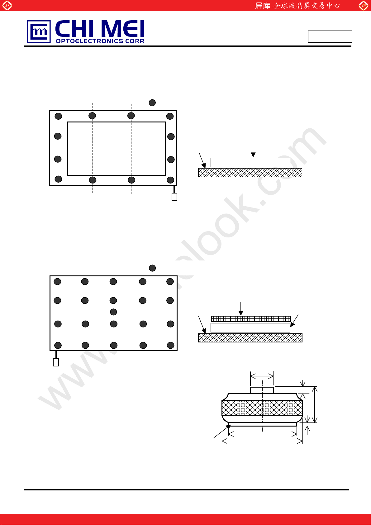
Fig 1-3-1
Fig 1-3-2
Fig 1-3-3
Non Operation
FL
R2
Non Operation
Definitions of failure for judgment shall be as follows:
1) Function of the module should be maintained.
2) Current consumption should be smaller than the specified value.
3) Appearance and display quality should not have distinguished degradation.
4) Luminance should be larger than the minimum value specified in optical specification.
6 / 26
One step solution for LCD / PDP / OLED panel application: Datasheet, inventory and accessory!
Version 3.1
www.panelook.com
Page 7
Global LCD Panel Exchange Center
NOTE
(1) The compression condition of front side
(a) Compression point : 12 points ( refer to Fig 1-3-1)
(b) Compression condition: Time 3 sec, Tool diameter: 16 mm in diameter (refer to Fig 1-3-3)
www.panelook.com
Issued Date: Apr. 19, 2004
Model No. : N141XB-L02
Approval
: COMPRESSION POINT
Flat plate
Fig 1-3-1
(2) The compression condition of rear side
(a) Compression point : 21 points ( refer to Fig 1-3-2 )
(b) Compression condition : Time 3 sec, Tool redius: 30 mm in diameter ( refer to Fig 1-3-3)
:COMPRESSION POINT
ABS natural 2.0t
Flat plate
LCD
LCD
Fig 1-3-2
(3) Dimension of the compression jig
(a) compression jig for front side A = 16 mm in diameter
B = 16 mm in diameter
(b) compression jig for rear side A = 30 mm in diameter
B = 28 mm in diameter
Rubber sheet
10 mm diameter
B
A
Fig 1-3-3
7 / 26
One step solution for LCD / PDP / OLED panel application: Datasheet, inventory and accessory!
10
16
1.5
Version 3.1
www.panelook.com
Page 8
Global LCD Panel Exchange Center
1.4 THE OTHERS
(1) Static electricity pressure resistance
Items Testing conditions Operation Non Operation
Contact discharge 150pF, 330 ohm
www.panelook.com
Issued Date: Apr. 19, 2004
Model No. : N141XB-L02
Approval
r10 kV r10 kV
Air discharge 150pF, 330 ohm
ESD Acceptance Definition:
Temporary performance degradation. Recovery by operator is acceptable. No hardware failure.
(2) Sound noise
There should be no uncomfortable noise.
Being used under whatever surrounds, when power on/off, the panel should not generate uncomfortable noise.
(3) Open / Short
No smoke, no firery at any open/ short test
(4) MTBF : 50000 Hr (except for backlight lamp)
r20 kV r20 kV
8 / 26
One step solution for LCD / PDP / OLED panel application: Datasheet, inventory and accessory!
Version 3.1
www.panelook.com
Page 9
Global LCD Panel Exchange Center
www.panelook.com
2. ELECTRICAL SPECIFICATIONS
2.1 TFT LCD MODULE
MODULE
Parameter Symbol
Power Supply Voltage VCC 3.0 3.3 3.6 V
“H” level LVDS signal input VIH - - +100 mV
“L” level LVDS signal input VIL -100 - - mV
White 300 330 380
Power Supply Current
Rush Current I
Ripple voltage VRP - - 100 mV
Terminating resistor Rt - 100 - Ohm
LCD Fuse name: Kamaya(manufacturer)
Black 400 450 500
Maximum
l
CC
RUSH
Min. Typ. Max.
450 500 550
- 1.0 1.5 A (2)
Value
Unit Notes
mA (10)
2.2 BACKLIGHT UNIT
Issued Date: Apr. 19, 2004
Model No. : N141XB-L02
Approval
(1)
(1)
LAMP : West, K-CB292-K-82KH
BACKLIGHT ( 1 Lamp)
Parameter Symbol
Lamp Voltage VL 576 640 704 V
Lamp Current IL 3.0 6.0 6.5 mA (3)
Startup Voltage VS
Operating Frequency FL 50 - 80 KHz (5)
Power Consumption PL - 3.84 - W (6), IL=6.0mA
Lamp Life time LBL 10000 15000 - Hrs (7)
Pin Symbol Description Remark
1 HV Lamp power input Pink
2 LV Ground Black
Connector Part No.: BHTR-02VS
User’s connector Part No.: SM02B-BHTS-B-TB
Min. Typ. Max.
- - 1360 (25oC) V
- - 1500 (0
The connector information of Black light unit.
Value
Unit Notes
IL=6.0mA
RMS
(4)
o
C) V
RMS
(4)
RMS
2.3 MATERIAL LIST CONCERNING EMI REGULATIONS
(1) EMI Regulations:
“N141XB-L02” which is assembled inside Toshiba’s Satellite model should be met to the regulations as
below:
CISPR: Pub.22 Class B
FCC : Part 15 Class B
VCCI
(2) Safety regulation (CMO TFT-LCD module only): UL 1950
: Class B
9 / 26
One step solution for LCD / PDP / OLED panel application: Datasheet, inventory and accessory!
Version 3.1
www.panelook.com
Page 10

Global LCD Panel Exchange Center
:
P
1. EMI Filter Silk Product Code Rating Maker
Bead L1, CMD5D11-100MC
Chip Resistor
2. DC/DC Converter Silk Osc. Freq. Maker
PWM IC U9 Typ 1.2 MHz. Maxim Technology
Note (1) Operating Temp. range is 0 ~ 50 ºC
L101,L102,R21
1, L401,L201
Note (2) Measurement Conditions
+3.3
+12V
47k
SW
1 k:
2SK14
www.panelook.com
10uH,+-20%,0.54
A,H=1.2mm(Max)
N/A 0 Ohm
Output To VCC (LCD module)
2SK1475
IF SW is High,
Output is 0V.
IF SW is Low,
Output is +3.3V
0.01
F / 50V
Issued Date: Apr. 19, 2004
Model No. : N141XB-L02
Approval
Sumida
VCC rising time is 5ms
Note (3) Lamp current is measured by utilizing a current meter for high frequency as shown below:
Note (4) The voltage shown above should be applied to the lamp for more than 1 second after startup.
Otherwise the lamp may not be turned on.
GND
LCD
Module
0.1VCC
Hot(Pink
GND(Black)
0.9VCC
5ms
)
3.3V
1
2
( Yokogawa 2016 )
A
Current meter
Inverter
Note (5) The lamp frequency may produce interference with horizontal synchronous frequency from the
display, and this may cause line flow on the display. In order to avoid interference the lamp
frequency should be detached from the horizontal synchronous frequency and its harmonics as far
as possible.
10 / 26
One step solution for LCD / PDP / OLED panel application: Datasheet, inventory and accessory!
Version 3.1
www.panelook.com
Page 11

Global LCD Panel Exchange Center
Note (6) PL = ILVL.
Note (7) The lifetime (Hr) of a lamp can be defined as the time in which it continues to operate under the
www.panelook.com
Issued Date: Apr. 19, 2004
Model No. : N141XB-L02
Approval
condition Ta = 252к and I
(1) When the brightness becomes 50% or lower than its original,
(2) When the effective ignition length becomes 80% or lower than its original value.
(Effective ignition length is defined as an area that has less than 70% brightness compared to the
brightness in the center point.)
Note (8) The waveform of the voltage output of inverter must be area-symmetric and the design of the
inverter must have specifications for the modularized lamp. The performance of the backlight, such
as lifetime or brightness, is greatly influenced by the characteristics of the DC-AC inverter for the
lamp. All the parameters of an inverter should be designed with care so as not to produce too much
current leakage from high-voltage output of the inverter. When designing or ordering the inverter,
please make sure that a poor lighting caused by the mismatch of the backlight and the inverter
(miss-lighting, flicker, etc.) never occurs. When the above situation is confirmed, the module should
be operated in the same manners as it is installed in your instrument.
= 6.0 mArms until one of the following event occurs :
L
Note (9) Vcc drop voltage that caused by rush current when sw-on ( refer to Note(2) test circuit ) is max.=0.5V
Note (10) The specified power supply current is under the conditions, Ta = 25 ± 2 ºC, fv = 60 Hz, whereas a power
dissipation check pattern below is displayed. The maximum value is measured when VCC=3.0V, the
typical value is measured when VCC=3.3V and the minimum value is measured when VCC=3.6V.
a. White Pattern
b. Black Pattern
Active Area
c. Maximum pattern (Zoom in)
RRGGBBRRGGB
RRGGBBRRGGB
B
B
BBR
R
BBR
R
…expend to whole active area
gray level = 0
gray level = 63
11 / 26
One step solution for LCD / PDP / OLED panel application: Datasheet, inventory and accessory!
Version 3.1
www.panelook.com
Page 12

Global LCD Panel Exchange Center
www.panelook.com
3. INTERFACE SPECIFICATIONS
3.1 THE PIN ASSIGNMENT OF LVDS INTERFACE CONNECTOR.
Pin Symbol Description Polarity Remark
1 Vss Ground
2 Vcc Power Supply +3.3 V (typical)
3 Vcc Power Supply +3.3 V (typical)
4 V
5 NC Non-Connection
6 CLK
7 DATA
8 Rxin0- LVDS Differential Data Input Negative
9 Rxin0+ LVDS Differential Data Input Positive
10 Vss Ground
11 Rxin1- LVDS Differential Data Input Negative
12 Rxin1+ LVDS Differential Data Input Positive
13 Vss Ground
14 Rxin2- LVDS Differential Data Input Negative
15 Rxin2+ LVDS Differential Data Input Positive
16 Vss Ground
17 CLK- LVDS Clock Data Input Negative
18 CLK+ LVDS Clock Data Input Positive
19 Vss Ground
20 NC Non-Connection
21 NC Non-Connection
22 Vss Ground
23 NC Non-Connection
24 NC Non-Connection
25 Vss Ground
26 NC Non-Connection
27 NC Non-Connection
28 Vss Ground
29 NC Non-Connection
30 NC Non-Connection
DDC 3.3V Power DDC 3.3V Power
EDID
DDC Clock DDC Clock
EDID
DDC Data DDC Data
EDID
Issued Date: Apr. 19, 2004
Model No. : N141XB-L02
Approval
R0~R5,G0
-
G1~G5,B0,B1
-
B2~B5,DE,Hsync,Vsync
LVDS Level Clock
Note (1) The first pixel is even.
Note (2) Connector Part No.: JAE-FI-XB30SL-HF10
Note (3) User’s connector Part No: JAE-FI-X30C2L
12 / 26
One step solution for LCD / PDP / OLED panel application: Datasheet, inventory and accessory!
Version 3.1
www.panelook.com
Page 13

Global LCD Panel Exchange Center
www.panelook.com
3.2 INPUT SIGNAL TIMING SPECIFICATIONS
The specifications of input signal timing are as the following table and timing diagram.
Signal Item Symbol Min. Typ. Max. Unit Note
DCLK Frequency 1/Tc 50 65 68 MHz -
Vertical Total Time TV 771 806 850 TH -
DE
Vertical Addressing Time TVD 768 768 768 TH -
Horizontal Total Time TH 1200 1344 1500 Tc -
Horizontal Addressing Time THD 1024 1024 1024 Tc -
Issued Date: Apr. 19, 2004
Model No. : N141XB-L02
Approval
INPUT SIGNAL TIMING DIAGRAM
DE
DCLK
T
DE
DATA
TVD
C
v
T
H
T
HD
T
13 / 26
One step solution for LCD / PDP / OLED panel application: Datasheet, inventory and accessory!
Version 3.1
www.panelook.com
Page 14

Global LCD Panel Exchange Center
3.3 COLOR DATA INPUT ASSIGNMENT
The brightness of each primary color (red, green and blue) is based on the 6-bit gray scale data input for the
color. The higher the binary input, the brighter the color. The table below provides the assignment of color
versus data input.
Color
R5 R4 R3 R2 R1 R0 G5 G4 G3 G2 G1 G0 B5 B4 B3 B2 B1 B0
Black
Red
Green
Basic
Colors
Gray
Scale
Of
Red
Gray
Scale
Of
Green
Gray
Scale
Of
Blue
Note (1) 0: Low Level Voltage, 1: High Level Voltage
Blue
Cyan
Magenta
Yellow
White
Red(0)/Dark
Red(1)
Red(2)
:
:
Red(61)
Red(62)
Red(63)
Green(0)/Dark
Green(1)
Green(2)
:
:
Green(61)
Green(62)
Green(63)
Blue(0)/Dark
Blue(1)
Blue(2)
:
:
Blue(61)
Blue(62)
Blue(63)
0
1
0
0
0
1
1
1
0
0
0
:
:
1
1
1
0
0
0
:
:
0
0
0
0
0
0
:
:
0
0
0
Red Green Blue
0
0
1
1
0
0
0
0
0
0
1
1
1
1
1
1
0
0
0
0
0
0
:
:
:
:
1
1
1
1
1
1
0
0
0
0
0
0
:
:
:
:
0
0
0
0
0
0
0
0
0
0
0
0
:
:
:
:
0
0
0
0
0
0
www.panelook.com
0
0
0
0
1
1
1
0
0
0
0
1
0
0
0
0
0
0
0
1
1
1
1
0
1
1
1
1
1
1
1
1
0
0
0
0
0
0
1
0
0
1
0
0
:
:
:
:
:
:
:
:
1
0
1
0
1
1
0
0
1
1
1
0
0
0
0
0
0
0
0
0
0
0
0
0
:
:
:
:
:
:
:
:
0
0
0
1
0
0
0
1
0
0
0
1
0
0
0
0
0
0
0
0
0
0
0
0
:
:
:
:
:
:
:
:
0
0
0
0
0
0
0
0
0
0
0
0
Data Signal
0
0
0
0
0
0
1
1
1
0
0
0
1
1
1
0
0
0
1
1
1
1
1
1
0
0
0
0
0
0
0
0
0
:
:
:
:
0
0
0
0
0
0
0
0
0
0
0
0
0
0
0
0
0
0
:
:
:
:
1
1
1
1
1
1
1
1
1
0
0
0
0
0
0
0
0
0
:
:
:
:
0
0
0
0
0
0
0
0
0
Issued Date: Apr. 19, 2004
Model No. : N141XB-L02
Approval
0
0
0
0
0
0
0
0
0
0
0
0
0
0
0
0
1
1
0
0
0
0
0
0
0
0
1
1
1
1
1
1
1
1
1
1
1
1
1
1
0
0
1
1
1
1
1
1
1
1
0
0
0
0
0
0
1
1
1
1
1
1
1
1
0
0
0
0
0
0
0
0
0
0
0
0
0
0
0
0
0
0
0
0
0
0
0
0
:
:
:
:
:
:
:
:
:
:
:
:
:
:
:
:
:
:
0
0
0
0
0
0
0
0
0
0
0
0
0
0
0
0
0
0
0
0
0
0
0
0
0
0
0
0
0
0
0
0
0
1
0
0
0
0
0
0
1
0
0
0
0
0
0
0
:
:
:
:
:
:
:
:
:
:
:
:
:
:
:
:
:
:
0
1
0
0
0
0
0
0
1
0
0
0
0
0
0
0
1
1
0
0
0
0
0
0
0
0
0
0
0
0
0
0
0
0
0
0
0
0
0
1
0
0
0
0
0
0
1
0
:
:
:
:
:
:
:
:
:
:
:
:
:
:
:
:
:
:
0
0
1
1
1
1
0
1
0
0
1
1
1
1
1
0
0
0
1
1
1
1
1
1
14 / 26
One step solution for LCD / PDP / OLED panel application: Datasheet, inventory and accessory!
Version 3.1
www.panelook.com
Page 15

Global LCD Panel Exchange Center
www.panelook.com
3.4 POWER UP/DOWN SEQUENCE & VCC DIP CONDITIONS
3.4.1 POWER UP/DOWN SEQUENCE
Power On
Power Off
Issued Date: Apr. 19, 2004
Model No. : N141XB-L02
Approval
Restart
Power Supply
for LCD, Vcc
- Interface Signal
(LVDS Signal of
Transmitter), V
- Power for Lamp
Timing Specifications:
470us Љ t1 Љ 10 msec
0 < t2 Љ 50 msec
0 < t3 Љ 50 msec
0V
0V
I
t4 Њ 500 msec
t5 Њ 100 msec
10%
90%
t1
90%
Valid Data
t6 t5
50%50%
ONOFF OFF
t4
10%
t3 t2
10%
t6 Њ 100 msec
Note (1) Please avoid floating state of interface signal at invalid period.
Note (2) When the interface signal is invalid, be sure to pull down the power supply of LCD Vcc to 0 V.
Note (3) The Backlight inverter power must be turned on after the power supply for the logic and the interface
signal is valid. The Backlight inverter power must be turned off before the power supply for the logic
and the interface signal is invalid.
15 / 26
One step solution for LCD / PDP / OLED panel application: Datasheet, inventory and accessory!
Version 3.1
www.panelook.com
Page 16

Global LCD Panel Exchange Center
3.4.2 VCC DIP CONDITIONS
www.panelook.com
Issued Date: Apr. 19, 2004
Model No. : N141XB-L02
Approval
Td
3.0 V
(1) 2.5VЉ VCC< 3.0V
TdЉ20 ms
(2) VCC< 2.5V
Vcc-Dip conditions also follow the power up/down conditions for supply voltage.
VCC
GND
16 / 26
One step solution for LCD / PDP / OLED panel application: Datasheet, inventory and accessory!
Version 3.1
www.panelook.com
Page 17

Global LCD Panel Exchange Center
www.panelook.com
Issued Date: Apr. 19, 2004
Model No. : N141XB-L02
Approval
4. OPTICAL SPECIFICATIONS
4.1 TEST CONDITIONS
Ambient Temperature : Ta = 25r2oC
Ambient Humidity : H
Supply Voltage : V
Input Signal : According to typical value in "Electrical Characteristics"
FL Input Current : I
FL Driving Frequency : f
FL Inverter : H05-4783B (Sumida)
The measuring method is shown in 4.2. The following items are measured under stable conditions. The optical
characteristics should be measured in a dark room ( Screen luminance < 2-lx ) or equivalent state with the methods
shown in Note (6).
4.2 OPTICAL SPECIFICATIONS
Item Symbol Conditions
Contrast Ratio CR
Response Time
Average luminance of
white ( 5 points )
Cross Modulation D
Red
Luminance
Uniformity
Chromaticity
Viewing Angle
13 Points White
Variation
13 Points CR Variation
White Variation dL
Green
Blue
White
Hor.
Ver.
Hor.
Ver.
50r10%RH
a
= 3.3V
DD
=6.0mArms
FL
= 60 kHz
FL
Specifications
Min. Typ. Max.
200 300 - - (2),(6)
AVE
TR - 6 10 ms
- 17 25 ms
T
F
130 170 - cd/m2
Y
L,AVE
Unit Note
(3)
=6.0mArms *
I
FL
Gray Scale
Level=L63 (White)
(4)
T
= TY =0q
- - 1.0 % (5)
SHA
Rx
Ry
Gx
Gy
Bx
By
Wx
Wy
TX+
T
X-
TY+
T
Y-
TX+
T
X-
TY+
T
Y-
ӬW
ӬC
R
X
Viewing normal angle
Center
CR>=10
Center
CR>=5
T
= TY =0q
X
Viewing normal angle
0.570
0.335
Typ.
-0.03
0.325
0.570
Typ.
+0.03
0.150
0.125
0.283 0.313 0.343
0.299 0.329 0.359
40 45 -
-
-
-
-
-
-
-
(1), (6)
40 45 15 20 35 40 50 55 -
deg.
50 55 25 30 40 45 -
- 1.3 1.6 - (7)
- 2.0 2.5 - (7)
- - 1.5 %/mm (8)
17 / 26
One step solution for LCD / PDP / OLED panel application: Datasheet, inventory and accessory!
Version 3.1
www.panelook.com
Page 18

Global LCD Panel Exchange Center
Item Symbol Conditions
63
60
56
52
48
44
40
36
Gamma
32
28
24
20
16
12
8
4
0
Viewing normal angle
T
= TY =0q
X
www.panelook.com
Min. Typ. Max.
100
83.4
65.6
51.7
40.4
32.1
25.0
19.1
14.2
10.5
7.4
4.8
2.8
1.4
0.5
0.1
0
Specifications
100
89.8
77.2
65.6
55.0
45.4
36.8
29.2
22.5
16.8
12.0
8.0
4.9
2.6
1.1
0.2
0
100
96.9
91.3
83.6
74.8
66.4
57.5
48.4
39.4
31.4
23.6
16.4
10.1
5.3
1.9
0.4
0
Issued Date: Apr. 19, 2004
Model No. : N141XB-L02
Approval
Unit Note
(1) (6)
%
at center of
Viewing area
center only
18 / 26
One step solution for LCD / PDP / OLED panel application: Datasheet, inventory and accessory!
Version 3.1
www.panelook.com
Page 19

Global LCD Panel Exchange Center
Note (1) Definition of Viewing Angle Tx and Ty :
www.panelook.com
Issued Date: Apr. 19, 2004
Model No. : N141XB-L02
Approval
TX- = 90º
x-
6 o’clock
T
y- = 90º
y-
Note (2) Definition of Contrast Ratio :
The contrast ratio can be calculated by the following expression.
Contrast Ratio (CR) = L63 / L0
L63 : Luminance on the white raster (gray scale level L63)
L 0 : Luminance on the black raster (gray scale level L0)
= ( CR(4)+CR(5)+CR(7)+CR(9)+CR(10) )/ 5
CR
AVE
CR(X) is correspond to the Contrast Ratio of a point of X at Figure of Note (7).
Note (3) Definition of Response time :
Normal
Tx = Ty = 0º
Ty- Ty
Tx
Tx
y+
12 o’clock direction
T
y+ = 90º
x+
TX+ = 90º
100%
90%
Optical
Response
10%
0%
White L63
TR
Black L0
TF
White L63
time
19 / 26
One step solution for LCD / PDP / OLED panel application: Datasheet, inventory and accessory!
Version 3.1
www.panelook.com
Page 20

Global LCD Panel Exchange Center
A
A
Note (4) Definition of Average Luminance of White :
measure the luminance of white at 5 points.
Average Luminance of White Y
Y
= ( Y L4+ Y L5+ Y L7+ Y L9+ Y
L,AVE
Y
is correspond to the Luminance of a point of X at Figure of Note (7).
LX
Note (5) Definition of Cross Modulation (D
D
= | YB – YA | / YA u100 (%)
SHA
Where :
Y
= Luminance of measured location without darkest gray pattern (cd/m2)
A
Y
= Luminance of measured location with darkest gray pattern (cd/m2)
B
L,AVE
SHA
www.panelook.com
) / 5
L10
)
Issued Date: Apr. 19, 2004
Model No. : N141XB-L02
Approval
(0, 0)
Y
(128, 384)
A,L
Y
(512, 672)
A, D
Gray 32
Note (6) Measuring setup :
The measurement suppose to be executed after stabilized the panel at given temperature during 30min. in the
case of abrupt temperature change. The measurement shall be executed 30 minutes after lighting at rating. The
luminance of white should be typical luminance ( Typical Condition IL=6.0mA ). In order to stable the luminance,
LCD shall not be gotten winds.
LCD module
LCD panel
ctive
Y
A, R
(1023, 767)
Center of the screen
Y
A
(896, 384)
Y
B, L
Y
B, D
(0, 0)
(256, 192)
(128, 384)
(512, 672)
ctive
Gray 0
Gray 32
Y
(512, 96)
B,U
Y
(896, 384)
B,R
(768, 576)
(1023, 767)
500 mm
Field of view = 2q
Photometer
(TOPCON BM-5A)
Light Shield Room
( Screen illuminance < 2-lx)
20 / 26
One step solution for LCD / PDP / OLED panel application: Datasheet, inventory and accessory!
Version 3.1
www.panelook.com
Page 21

Global LCD Panel Exchange Center
www.panelook.com
Note (7) Definition of 13 points white variation GW, CR variation GC
R
GW = Maximum luminance of 13 points / Minimum luminance of 13 points
= Maximum CR 13 points / Minimum CR of 13 points
GC
R
0 255 511 767 1023
0
45
191
383
575
Vertical Line number
722
767
Horizontal Line number
45
3
12 11
10
9
8
7 6
5 4
3 2 1
Active area
978
Note (8) Definition of White Variation dL : measure the luminance of white at 13 u11 p oints .
dL = | L(x,y) – L(x+I, y+j)| / ( L(x,y) u D(x+I, y+j) ) u100 (%/mm)
where 2 d x d 12, 2 d y d 10, I = r 1, j = r 1
Issued Date: Apr. 19, 2004
Model No. : N141XB-L02
Approval
: test point
11 points
13
8.75 8.75
8.75
I17.5mm
8.75
Active area
Measuring Spot
( Field of View : 2deg. Measuring Distance : 500mm)
I17.5mm
L(x-1,y-1)
D(x+1,y-1)
L(x+1,y-1)
L(x,y)
L(x+1,y+1)
21 / 26
One step solution for LCD / PDP / OLED panel application: Datasheet, inventory and accessory!
Version 3.1
www.panelook.com
Page 22

Global LCD Panel Exchange Center
www.panelook.com
Issued Date: Apr. 19, 2004
Model No. : N141XB-L02
Approval
5. MECHNICAL DRAWING
Please refer to the attached drawings.
6. PRECAUTION
6. 1 ASSEMBLY AND HANDLING PRECAUTION
(1) Do not apply rough force such as bending or twisting to the module during assembly.
(2) To assemble or install module into user’s system can be only in clean working areas. The dust and oil may cause
electrical short or worsen the polarizer.
(3) It’s not permitted to have pressure or impulse on the module because the LCD panel and backlight will be damaged.
(4) Always follow the correct power sequence when LCD module is connecting and operating. This can prevent damage
to the CMOS LSI chips during latchup.
(5) Do not pull the I/F connector in or out while the module is operating.
(6) Do not disassemble the module.
(7) Use a soft dry cloth without chemicals for cleaning, because the surface of polarizer is very soft and easily scratched.
(8) It is dangerous that moisture come into or contacted the LCD module, because moisture may damage LCD module
when it is operating.
(9) High temperature or humidity may reduce the performance of module. Please store LCD module within the specified
storage conditions.
(10) When ambient temperature is lower than 10ºC may reduce the display quality. For example, the response time will
become slowly, and the starting voltage of CCFL will be higher than room temperature.
6.2 SAFTY PRECAUTION
(1) The startup voltage of backlight is approximately 1000 Volts. It may cause electrical shock while assembling with
inverter. Do not disassemble the module or insert anything into the backlight unit.
(2) If the liquid crystal material leaks from the panel, it should be kept away from the eyes or mouth. In case of contact
with hands, skin or clothes, it has to be washed away thoroughly with soap.
22 / 26
One step solution for LCD / PDP / OLED panel application: Datasheet, inventory and accessory!
Version 3.1
www.panelook.com
Page 23

Global LCD Panel Exchange Center
www.panelook.com
7. PACKAGING
7.1 PACKING SPECIFICATIONS
(1) 20 LCD modules / 1 Box
(2) Box dimensions : 511(L) X 420(W) X 360(H) mm
(3) Weight : approximately 11.3Kg (20 modules per box)
7.2 PACKING METHOD
(1)Carton Packing should have no failure in the following reliability test items.
Test Item Test Conditions Note
Frequency Range: 5 – 50 Hz, Degree of acceleration 9.8 m/s
Vibration
Dropping Test 1 Angle, 3 Edge, 6 Face, 60cm Non Operation
Sweep rate 3 minutes
Top & Bottom 60 minutes, Right & Left 15 minutes, Back & Forth 15
minutes
2
(1G).
Issued Date: Apr. 19, 2004
Model No. : N141XB-L02
Approval
Non Operation
(2) The Figure. 7-1,2 show the packing method.
Figure. 7-1 Packing method (Carton)
23 / 26
One step solution for LCD / PDP / OLED panel application: Datasheet, inventory and accessory!
Version 3.1
www.panelook.com
Page 24

Global LCD Panel Exchange Center
www.panelook.com
Issued Date: Apr. 19, 2004
Model No. : N141XB-L02
Approval
Figure. 7-2 Packing method (Pallet)
24 / 26
One step solution for LCD / PDP / OLED panel application: Datasheet, inventory and accessory!
Version 3.1
www.panelook.com
Page 25

Global LCD Panel Exchange Center
www.panelook.com
Issued Date: Apr. 19, 2004
Model No. : N141XB-L02
8. DEFINITION OF SHIPPING LABEL ON MODULE
(1) CMO Label
The barcode nameplate is pasted on each module as illustration, and its definitions are as following explanation.
Approval
01A
G33C0001Z110
N141XB -L02
N141X5 - L03 Rev.XX
X X X X X X X Y M D L N N N N
C P 1 3 5 4 4 8 - 0 1
E207943
MADE IN TAIWAN
(70mm x 24mm)
(a) Model Name: N141XB - L02
(b) Revision: Rev. XX, for example: A1, …, C1, C2 …etc.
(c) Serial ID: X X
Serial ID includes the information as below:
(a) Manufactured Date: Year: 1~9, for 2001~2009
X X X X X Y M D X N N N N
Month: 1~9, A~C, for Jan. ~ Dec.
Day: 1~9, A~Y, for 1
st
Serial No.
CMO Internal Use
Year, Month, Date
CMO Internal Use
Revision
CMO Internal Use
to 31st, exclude I , O and U
(b) Revision Code: cover all the change
(c) Serial No.: Manufacturing sequence of product
25 / 26
One step solution for LCD / PDP / OLED panel application: Datasheet, inventory and accessory!
Version 3.1
www.panelook.com
Page 26

Global LCD Panel Exchange Center
(2) Carton Label
www.panelook.com
Issued Date: Apr. 19, 2004
Model No. : N141XB-L02
Approval
(3) Pallet Label
VF2093P01
G33C0001Z110
G33C0001Z110
VF2093P01
26 / 26
One step solution for LCD / PDP / OLED panel application: Datasheet, inventory and accessory!
Version 3.1
www.panelook.com
Page 27

Global LCD Panel Exchange Center
www.panelook.com
One step solution for LCD / PDP / OLED panel application: Datasheet, inventory and accessory!
www.panelook.com
 Loading...