

CMO N133I6-L08 Specification

Global LCD Panel Exchange Center
ுழၴ ຝ ᐉு ߡۥ ދป
ขጥ
A
徐
凡 琇
TFT LCD Approval Specification
MODEL NO.: N133I6 – L08
Customer:
pproved by:
www.panelook.com
Doc No.: 400028601
Issued Date: March. 24, 2009
Model No.: N133I6 - L08
Approval
Note:
2009.04.08
Director Accept
2009-04-08
NB
13:34:23
1 / 28
The information described in this technical specification is tentative and it is possible to be changed without prior
notice. Please contact CMO ’s representative while your product design is based on this specification.
One step solution for LCD / PDP / OLED panel application: Datasheet, inventory and accessory!
Version 2.0
www.panelook.com
Global LCD Panel Exchange Center
www.panelook.com
Doc No.: 400028601
Issued Date: March. 24, 2009
Model No.: N133I6 - L08
Approval
- CONTENTS -
REVISION HISTORY ------------------------------------------------------- 3
1. GENERAL DESCRIPTION
1.1 OVERVIEW
1.2 FEATURES
1.3 APPLICATION
1.4 GENERAL SPECIFICATIONS
1.5 MECHANICAL SPECIFICATIONS
------------------------------------------------------- 4
2. ABSOLUTE MAXIMUM RATINGS ------------------------------------------------------- 5
2.1 ABSOLUTE RATINGS OF ENVIRONMENT
2.2 ELECTRICAL ABSOLUTE RATINGS
2.2.1 TFT LCD MODULE
2.2.2 BACKLIGHT UNIT
3. ELECTRICAL CHARACTERISTICS ------------------------------------------------------- 7
3.1 TFT LCD MODULE
3.2 BACKLIGHT UNIT
4. BLOCK DIAGRAM ------------------------------------------------------- 11
4.1 TFT LCD MODULE
4.2 BACKLIGHT UNIT
5. INPUT TERMINAL PIN ASSIGNMENT ------------------------------------------------------- 12
5.1 TFT LCD MODULE
5.2 BACKLIGHT UNIT
5.3 TIMING DIAGRAM OF LVDS INPUT SIGNAL
5.4 COLOR DATA INPUT ASSIGNMENT
6. INTERFACE TIMING
6.1 INPUT SIGNAL TIMING SPECIFICATIONS
6.2 POWER ON/OFF SEQUENCE
7. OPTICAL CHARACTERISTICS
7.1 TEST CONDITIONS
7.2 OPTICAL SPECIFICATIONS
8. PRECAUTIONS
8.1 HANDLING PRECAUTIONS
8.2 STORAGE PRECAUTIONS
8.3 OPERATION PRECAUTIONS
------------------------------------------------------- 16
------------------------------------------------------- 18
------------------------------------------------------- 22
9. PACKING ------------------------------------------------------- 23
9.1 CARTON
9.2 PALLET
10. DEFINITION OF LABELS
10.1 CMO MODULE LABEL
10.2 CMO CARTON LABE
10.3 CUSTOMER CARTON LABEL
10.4 CUSTOMER PALLET LABEL
------------------------------------------------------- 25
2 / 28
The information described in this technical specification is tentative and it is possible to be changed without prior
notice. Please contact CMO ’s representative while your product design is based on this specification.
One step solution for LCD / PDP / OLED panel application: Datasheet, inventory and accessory!
Version 2.0
www.panelook.com

Global LCD Panel Exchange Center
www.panelook.com
Doc No.: 400028601
Issued Date: March. 24, 2009
Model No.: N133I6 - L08
Approval
REVISION HISTORY
Version Date
1.0
2.0
Dec, 15,’08
Mar. 24, ‘09
Page
(New)
All
All
Section Description
All
Preliminary specification was first issued.
All
Approval specification was first issued.
3 / 28
The information described in this technical specification is tentative and it is possible to be changed without prior
notice. Please contact CMO ’s representative while your product design is based on this specification.
One step solution for LCD / PDP / OLED panel application: Datasheet, inventory and accessory!
Version 2.0
www.panelook.com
Global LCD Panel Exchange Center
1. GENERAL DESCRIPTION
1.1 OVERVIEW
N133I6 – L08 is a 13.3” TFT Liquid Crystal Display module with LED Backlight unit and 30 pins LVDS
interface. This module supports 1280 x 800 WXGA mode and can display 262,144 colors. The optimum
viewing angle is at 6 o’clock direction. The converter module for Backlight is not built in.
1.2 FEATURES
- Thin and Light Weight
- WXGA (1280 x 800 pixels) resolution
- DE only mode
- 3.3V LVDS (Low Voltage Differential Signaling) interface with 1 pixel/clock
www.panelook.com
Doc No.: 400028601
Issued Date: March. 24, 2009
Model No.: N133I6 - L08
Approval
1.3 APPLICATION
- TFT LCD Notebook
1.4 GENERAL SPECIFICATI0NS
Item Specification Unit Note
Active Area 286.08 (H) x 178.8 (V) mm
CF Polarizer 289.38 (H) x 182.3 (V) mm
Driver Element a-si TFT active matrix - Pixel Number 1280 x R.G.B. x 800 pixel Pixel Pitch 0.2235 (H) x 0.2235 (V) mm Pixel Arrangement RGB vertical stripe - Display Colors 262,144 color Transmissive Mode Normally white - Surface Treatment Glare, LT4 , 3H - -
1.5 MECHANICAL SPECIFICATIONS
Item Min. Typ. Max. Unit Note
Horizontal(H) 296.85 297.15 297.45 mm
Module Size
I/F connector mounting position The mounting inclination of the connector makes the screen
Note (1) Please refer to the attached drawings for more information of front and back outline dimensions.
Vertical(V) 202.8 203.2 203.6 mm
Depth(D) 3.08 3.38 3.68 mm
Weight -- -- 310 g -
center within ±0.5mm as the horizontal.
(1)
(1)
(2)
Note (2) Connector mounting position
+/- 0.5mm
4 / 28
The information described in this technical specification is tentative and it is possible to be changed without prior
notice. Please contact CMO ’s representative while your product design is based on this specification.
One step solution for LCD / PDP / OLED panel application: Datasheet, inventory and accessory!
Version 2.0
www.panelook.com
Global LCD Panel Exchange Center
A
2. ABSOLUTE MAXIMUM RATINGS
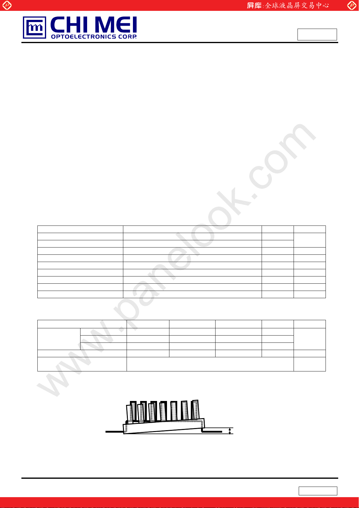
2.1 ABSOLUTE RATINGS OF ENVIRONMENT
Item Symbol
Storage Temperature TST -20 +60 ºC (1)
Operating Ambient Temperature TOP 0 +50 ºC (1), (2)
Shock (Non-Operating) S
Vibration (Non-Operating) V
Note (1) Temperature and relative humidity range is shown in the figure below.
(a) 90 %RH Max. (Ta Љ 40 ºC).
(b) Wet-bulb temperature should be 39 ºC Max. (Ta > 40 ºC).
(c) No condensation.
www.panelook.com
Doc No.: 400028601
Issued Date: March. 24, 2009
Model No.: N133I6 - L08
Approval
Value
Min. Max.
- 220/2 G (3), (5)
NOP
- 1.5 G (4), (5)
NOP
Unit Note
Relative Humidity (%RH)
100
90
80
60
Operating Range
40
20
10
Storage Range
Temperature (ºC)
Note (2) The temperature of panel surface should be 0 ºC Min. and 50 ºC Max.
8060-20 40 0 20 -40
Note (3) 1 time for ± X, ± Y, ± Z. for Condition (220G / 2ms) is half Sine Wave,.
Note (4) 10 ~ 500 Hz, 0.5 Hr / Cycle, 1 cycles for each X, Y, Z.
Note (5) At testing Vibration and Shock, the fixture in holding the module has to be hard and rigid enough
so that the module would not be twisted or bent by the fixture.
The fixing condition is shown as below:
t Room Temperature
5 / 28
The information described in this technical specification is tentative and it is possible to be changed without prior
notice. Please contact CMO ’s representative while your product design is based on this specification.
One step solution for LCD / PDP / OLED panel application: Datasheet, inventory and accessory!
Version 2.0
www.panelook.com
Global LCD Panel Exchange Center
2.2 ELECTRICAL ABSOLUTE RATINGS
2.2.1 TFT LCD MODULE
Item Symbol
Power Supply Voltage VCC -0.3 +4.0 V
Logic Input Voltage VIN -0.3 VCC+0.3 V
2.2.2 BACKLIGHT UNIT
Item
LED Light Bar Power Supply Voltage -45 31.5 V
LED Light Bar Power Supply Current 0 150 mA
Note (1) Permanent damage to the device may occur if maximum or minimum values are exceeded.
Function operation should be restricted to the conditions described under Normal Operating Conditions.
www.panelook.com
Value
Min. Max.
Value
Min Max.
Unit Note
Doc No.: 400028601
Issued Date: March. 24, 2009
Model No.: N133I6 - L08
Approval
(1)
Unit Note
(1)
6 / 28
The information described in this technical specification is tentative and it is possible to be changed without prior
notice. Please contact CMO ’s representative while your product design is based on this specification.
One step solution for LCD / PDP / OLED panel application: Datasheet, inventory and accessory!
Version 2.0
www.panelook.com
Global LCD Panel Exchange Center
www.panelook.com
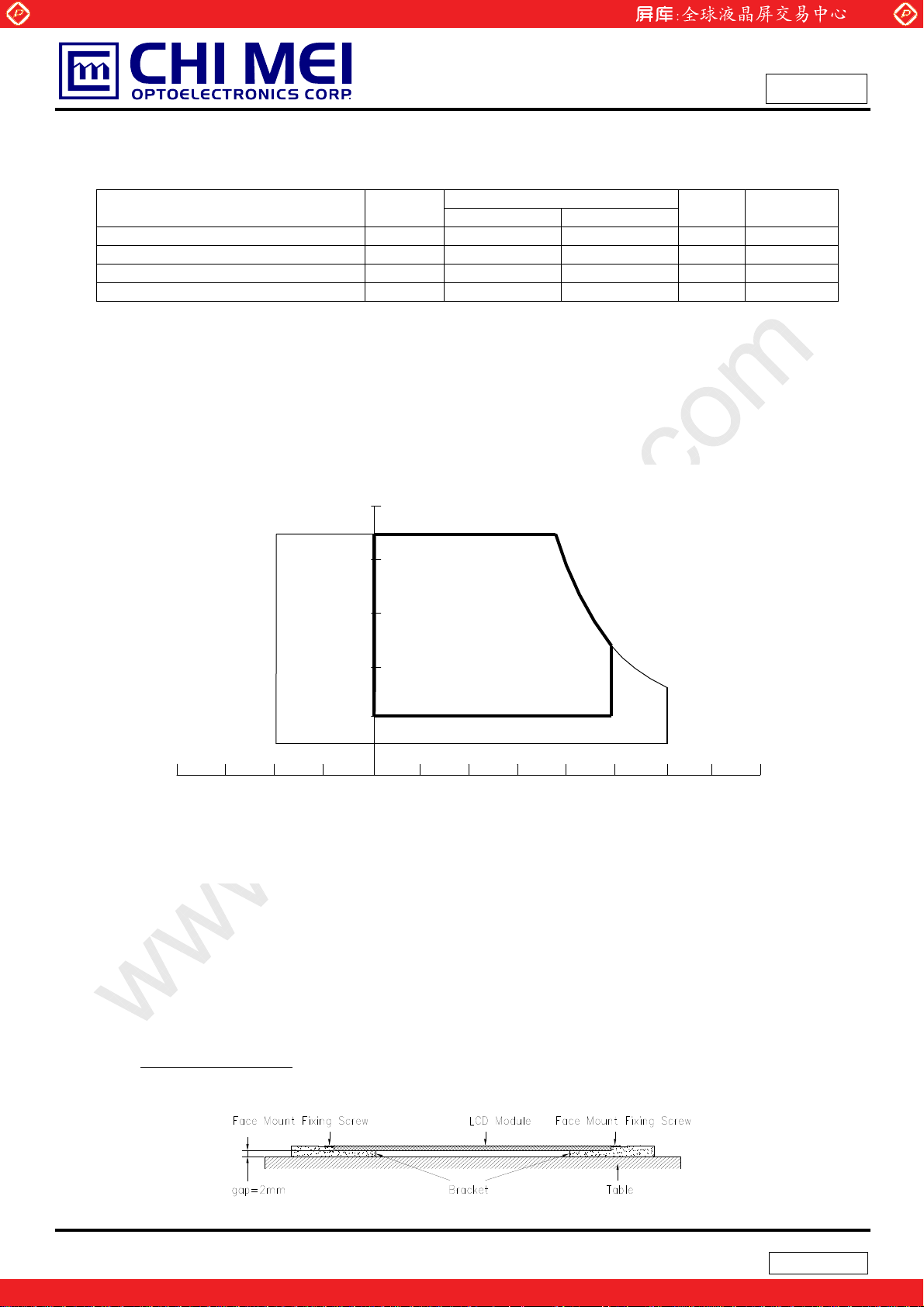
3. ELECTRICAL CHARACTERISTICS
3.1 TFT LCD MODULE
Parameter Symbol
Min. Typ. Max.
Power Supply Voltage Vcc 3.0 3.3 3.6 V Permissive Ripple Voltage VRP - 50 - mV Rush Current I
- - 1.5 A (2)
RUSH
Initial Stage Current IIS - - 1.0 A (2)
Power Supply Current
LVDS Differential Input High Threshold V
LVDS Differential Input Low Threshold V
White - 190 220 mA (3)a
Black
Icc
TH(LVDS)
TL(LVDS)
- 250 280 mA (3)b
- - +100 mV
-100 - - mV
LVDS Common Mode Voltage VCM 1.125 - 1.375 V (5)
LVDS Differential Input Voltage |VID| 100 - 600 mV (5)
Terminating Resistor RT - 100 - Ohm
Power per EBL WG P
- 1.40 - W (4)
EBL
Note (1) The ambient temperature is Ta = 25 ± 2 ºC.
Value
Doc No.: 400028601
Issued Date: March. 24, 2009
Model No.: N133I6 - L08
Approval
Unit Note
(5),
=1.2V
V
CM
(5)
=1.2V
V
CM
Note (2) I
I
: the maximum current when VCC is rising
RUSH
: the maximum current of the first 100ms after power-on
IS
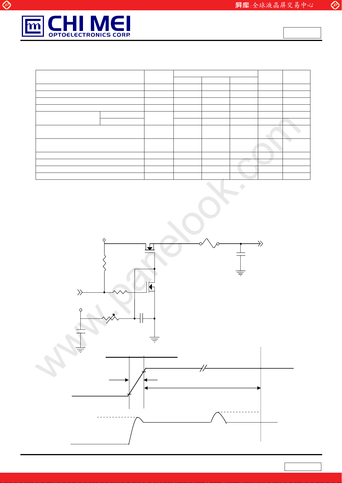
Measurement Conditions: Shown as the following figure. Test pattern: black.
(High to Low)
(Control Signal)
SW
+12V
+3.3V
R1
47K
R2
1K
47K
VR1
C1
1uF
Q1 2SK1475
C2
0.01uF
Q2
2SK1470
FUSE
C3
1uF
Vcc rising time is 470us
+3.3V
0.9Vcc
Vcc
(LCD Module Input)
VCC
100ms
I
IS
0V
I
RUSH
470us
0.1Vcc
ICC
7 / 28
The information described in this technical specification is tentative and it is possible to be changed without prior
notice. Please contact CMO ’s representative while your product design is based on this specification.
One step solution for LCD / PDP / OLED panel application: Datasheet, inventory and accessory!
Version 2.0
www.panelook.com
Global LCD Panel Exchange Center
|
|
)
)
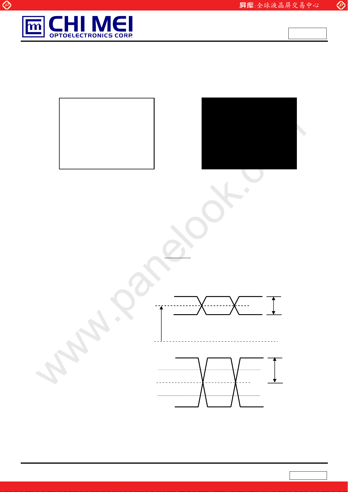
Note (3) The specified power supply current is under the conditions at Vcc = 3.3 V, Ta = 25 ± 2 ºC, fv = 60
Hz, whereas a power dissipation check pattern below is displayed.
www.panelook.com
Doc No.: 400028601
Issued Date: March. 24, 2009
Model No.: N133I6 - L08
Approval
a. White Pattern
Active Area
b. Black Pattern
Active Area
Note (4) The specified power are the sum of LCD panel electronics input power and the converter input
power. Test conditions are as follows.
(a) Vcc = 3.3 V, Ta = 25 ± 2 ºC, f
= 60 Hz,
v
(b) The pattern used is a black and white 32 x 36 checkerboard, slide #100 from the VESA file
“Flat Panel Display Monitor Setup Patterns”, FPDMSU.ppt.
(c) Luminance: 60 nits.
(d) The converter used is provided from CMO tool.
Please contact them for detail information.
CMO doesn’t provide the converter in this product.
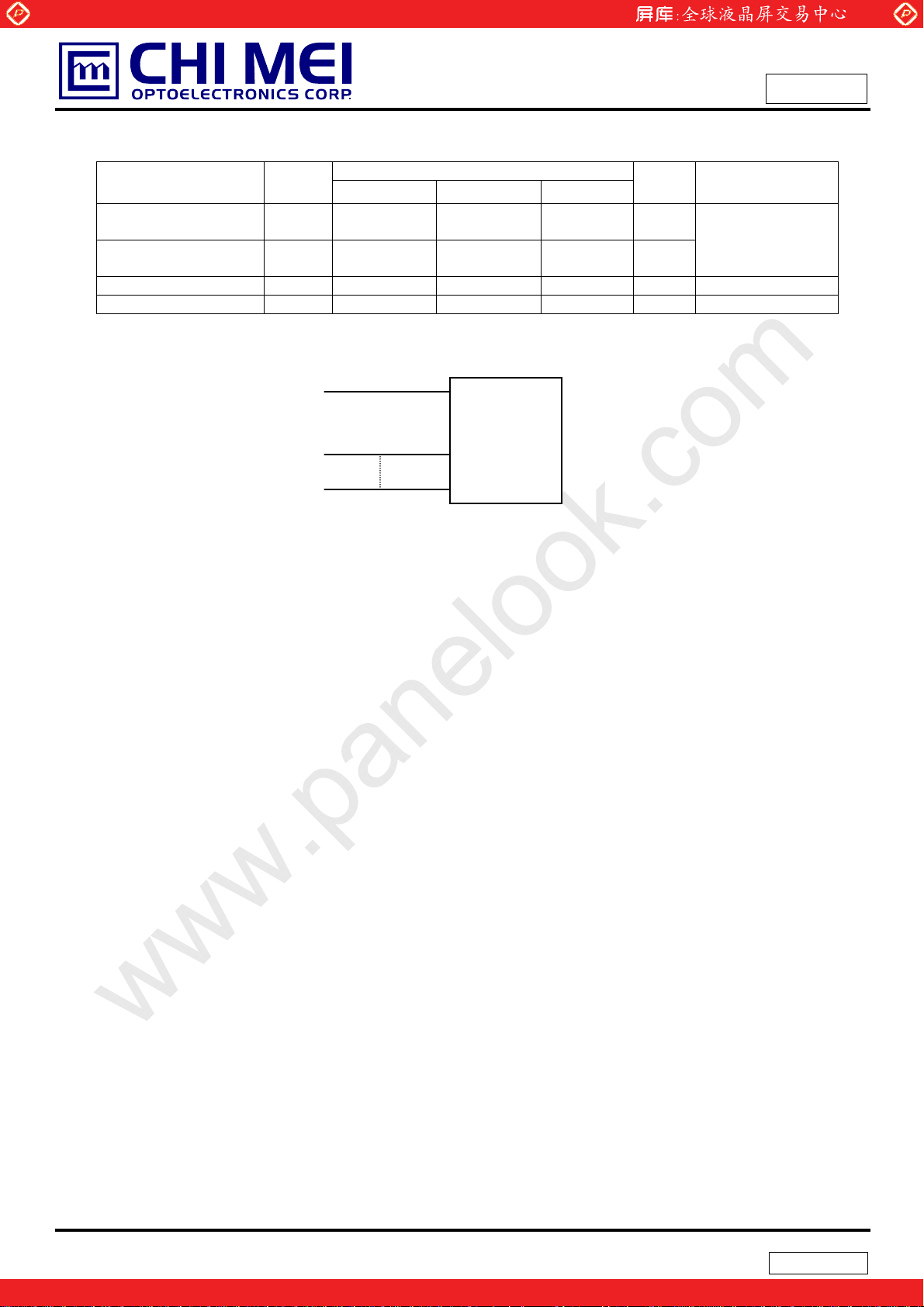
Note (5) The parameters of LVDS signals are defined as the following figures.
CM
V
Single Ended
0V
V
TH(LVD S
Differential
0V
V
TL(LVD S
VID
|VID|
8 / 28
The information described in this technical specification is tentative and it is possible to be changed without prior
notice. Please contact CMO ’s representative while your product design is based on this specification.
One step solution for LCD / PDP / OLED panel application: Datasheet, inventory and accessory!
Version 2.0
www.panelook.com
Global LCD Panel Exchange Center
www.panelook.com
Doc No.: 400028601
Issued Date: March. 24, 2009
Model No.: N133I6 - L08
3.2 BACKLIGHT UNIT Ta = 25 ± 2 ºC
Parameter Symbol
LED Light Bar Power
Supply Voltage
LED Light Bar Power
Supply Current
27.4 28.8 30.2 V
V
L
114 120 126 mA
I
L
Min. Typ. Max.
Power Consumption PL 3.12 3.46 3.80 W (3), (Duty 100%)
LED Life Time LBL 10000 -- -- Hrs (4)
Note (1) LED light bar configuration is shown as below.
VL,I
L
Light Bar Feedback
Value
LED
Light Bar
Unit Note
(1),(2) (Duty 100%)
Approval
Channels
Note (2) For better LED light bar driving quality, it is recommended to utilize the adaptive boost converter with current
balancing function to drive LED light-bar.
Note (3) P
Note (4) The lifetime of LED is defined as the time when it continues to operate under the conditions at Ta = 25 2
= I
L
LVL
and I
= 20 mA(Per EA) until the brightness becomes Љ 50% of its original value.
L
o
C
9 / 28
The information described in this technical specification is tentative and it is possible to be changed without prior
notice. Please contact CMO ’s representative while your product design is based on this specification.
One step solution for LCD / PDP / OLED panel application: Datasheet, inventory and accessory!
Version 2.0
www.panelook.com
 Loading...