

Page 1
Global LCD Panel Exchange Center
www.panelook.com
One step solution for LCD / PDP / OLED panel application: Datasheet, inventory and accessory!
www.panelook.com
TFT LCD Preliminary Specification
MODEL NO.: N133I6 - L01
Doc No.:
Issued Date: Feb. 25, 2008
Model No.: N133I6 - L01
Preliminary
Customer: Apple/ QSMC
Approved by:
Note:
記錄 工作 審核 角色 投票
2008-03-28
19:54:28 CST
PMMD
Director
cs_lee(李志聖
Director Accept
/56510/44926)
1 / 30
The information described in this technical specification is tentative and it is possible to be changed without prior
notice. Please contact CMO ’s representative while your product design is based on this specification.
Version 1.0
Page 2
Global LCD Panel Exchange Center
www.panelook.com
One step solution for LCD / PDP / OLED panel application: Datasheet, inventory and accessory!
www.panelook.com
Doc No.:
Issued Date: Feb. 25, 2008
Model No.: N133I6 - L01
Preliminary
- CONTENTS -
REVISION HISTORY
1. GENERAL DESCRIPTION
1.1 OVERVIEW
1.2 FEATURES
1.3 APPLICATION
1.4 GENERAL SPECIFICATIONS
1.5 MECHANICAL SPECIFICATIONS
2. ABSOLUTE MAXIMUM RATINGS
2.1 ABSOLUTE RATINGS OF ENVIRONME NT
2.2 ELECTRICAL ABSOLUTE RATINGS
2.2.1 TFT LCD MODULE
2.2.2 BACKLIGHT UNIT
3. ELECTRICAL CHARACTERISTICS
3.1 TFT LCD MODULE
3.2 BACKLIGHT UNIT
4. BLOCK DIAGRAM
4.1 TFT LCD MODULE
4.2 BACKLIGHT UNIT
5. INPUT TERMINAL PIN ASSIGNMENT
5.1 TFT LCD MODULE
5.2 BACKLIGHT UNIT
5.3 TIMING DIAGRAM OF LVDS INPUT SIGNAL
5.4 COLOR DATA INPUT ASSIGNMENT
5.5 EDID DATA STRUCTURE
6. INTERFACE TIMING
6.1 INPUT SIGNAL TIMING SPECIFICATIONS
6.2 POWER ON/OFF SEQUENCE
7. OPTICAL CHARACTERISTICS
7.1 TEST CONDITIONS
7.2 OPTICAL SPECIFICATIONS
8. PRECAUTIONS
8.1 HANDLING PRECAUTIONS
8.2 STORAGE PRECAUTIONS
8.3 OPERATION PRECAUTIONS
9. PACKING ------------------------------------------------------- 23
9.1 CARTON
9.2 PALLET
10. DEFINITION OF LABELS
10.1 CMO MODULE LABEL
10.2 CMO CARTON LABE
10.3 CUSTOMER CARTON LABEL
10.4 CUSTOMER PALLET LABEL
------------------------------------------------------- 3
------------------------------------------------------- 4
------------------------------------------------------- 5
------------------------------------------------------- 7
------------------------------------------------------- 11
------------------------------------------------------- 12
------------------------------------------------------- 16
------------------------------------------------------- 18
------------------------------------------------------- 22
------------------------------------------------------- 25
2 / 30
The information described in this technical specification is tentative and it is possible to be changed without prior
notice. Please contact CMO ’s representative while your product design is based on this specification.
Version 1.0
Page 3
Global LCD Panel Exchange Center
www.panelook.com
One step solution for LCD / PDP / OLED panel application: Datasheet, inventory and accessory!
www.panelook.com
Doc No.:
Issued Date: Feb. 25, 2008
Model No.: N133I6 - L01
Preliminary
Version Date
1.0
Feb, 25,’08 All All Preliminary specification was first issued.
Page
(New)
REVISION HISTORY
Section Description
3 / 30
The information described in this technical specification is tentative and it is possible to be changed without prior
notice. Please contact CMO ’s representative while your product design is based on this specification.
Version 1.0
Page 4
Global LCD Panel Exchange Center
www.panelook.com
One step solution for LCD / PDP / OLED panel application: Datasheet, inventory and accessory!
www.panelook.com
1. GENERAL DESCRIPTION
1.1 OVERVIEW
N133I6 - L01 is a 13.3” TFT Liquid Crystal Display module with 54 LED Backlight unit and 30 pins LVDS
interface. This module supports 1280 x 800 WXGA mode and can display 262,144 colors. The optimum
viewing angle is at 6 o’clock direction. The converter module for Backlight is not built in.
1.2 FEATURES
- Thin and Light Weight
- WXGA (1280 x 800 pixels) resolution
- DE only mode
- 3.3V LVDS (Low Voltage Differential Signaling) interface with 1 pixel/clock
Doc No.:
Issued Date: Feb. 25, 2008
Model No.: N133I6 - L01
Preliminary
1.3 APPLICA TION
- TFT LCD Notebook
1.4 GENERAL SPECIFICATI0NS
Item Specification Unit Note
Active Area 286.08 (H) x 178.8 (V) mm
CF Polarizer 289.48 (H) x 182.2 (V) mm
Driver Element a-si TFT active matrix - Pixel Number 1280 x R.G.B. x 800 pixel Pixel Pitch 0.2235 (H) x 0.2235 (V) mm Pixel Arrangement RGB vertical stripe - Display Colors 262,144 color Transmissive Mode Normally white - Surface Treat ment Glare , 3H - -
1.5 MECHANICAL SPECIFICATIONS
Item Min. Typ. Max. Unit Note
Horizontal(H) 296.85 297.15 297.45 mm
Module Size
I/F connector mounting position The mounting inclination of the connector makes the screen
Note (1) Please refer to the attached drawings for more information of front and back outline dimensions.
Vertical(V) -- 203.15 -- mm
Depth(D) -- -- 3.045 mm
Weight --- 216 219 g -
center within ±0.5mm as the horizontal.
(1)
(1)
(2)
Note (2) Connector mounting position
+/- 0.5mm
4 / 30
The information described in this technical specification is tentative and it is possible to be changed without prior
notice. Please contact CMO ’s representative while your product design is based on this specification.
Version 1.0
Page 5
Global LCD Panel Exchange Center
www.panelook.com
One step solution for LCD / PDP / OLED panel application: Datasheet, inventory and accessory!
www.panelook.com
2. ABSOLUTE MAXIMUM RATINGS
2.1 ABSOLUTE RATINGS OF ENVIRONMENT
Item Symbol
Storage Temperature TST -20 +60 ºC (1)
Operating Ambient T emperature TOP 0 +50 ºC (1), (2)
Shock (Non-Operating) S
Vibration (Non-Operating) V
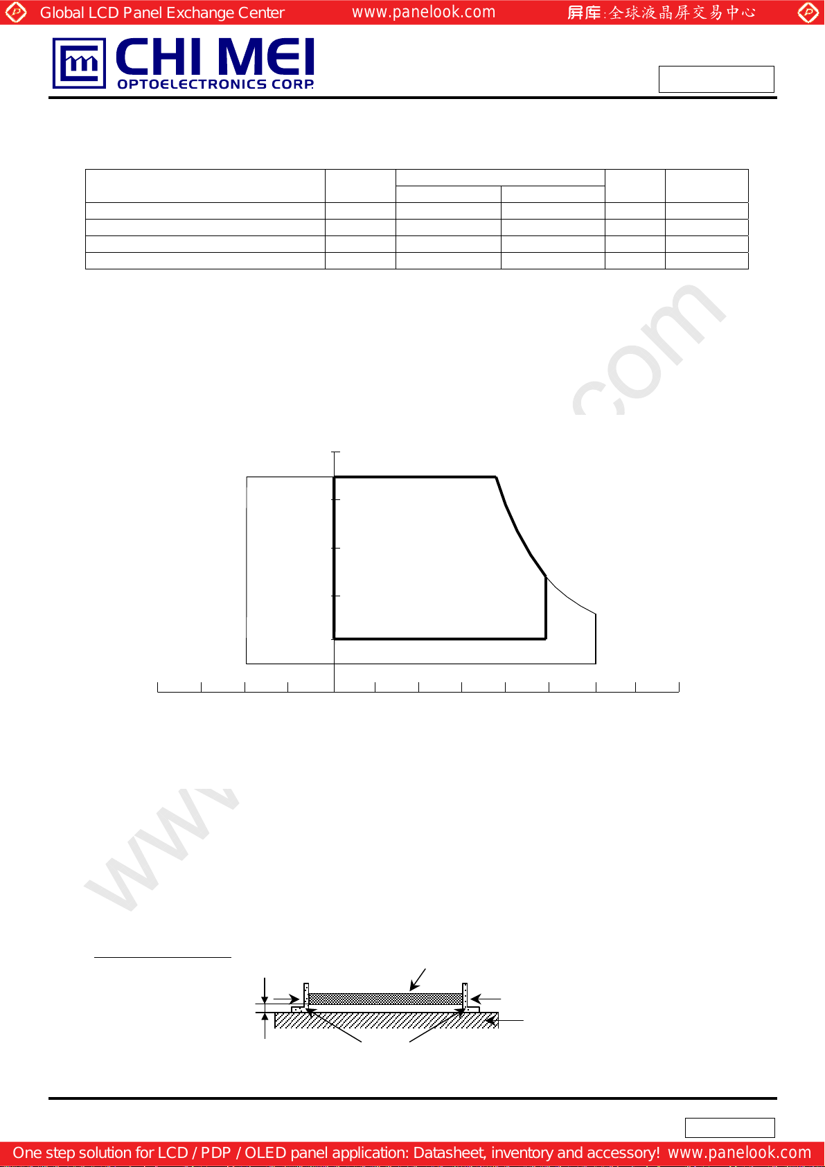
Note (1) Temperature and relative humidity range is shown in the figure below.
(a) 90 %RH Max. (Ta ≦ 40 ºC).
(b) Wet-bulb temperature should be 39 ºC Max. (Ta > 40 ºC).
(c) No condensation.
Doc No.:
Issued Date: Feb. 25, 2008
Model No.: N133I6 - L01
Preliminary
Value
Min. Max.
- 200/2 G (3), (5)
NOP
- 1.5 G (4), (5)
NOP
Unit Note
Relative Humidity (%RH)
100
90
80
60
Operating Range
40
20
10
Storage Range
Temperature (ºC)
Note (2) The temperature of panel surface should be 0 ºC Min. and 50 ºC Max.
8060 -20 400 20-40
Note (3) 1 time for ± X, ± Y, ± Z. for Condition (200G / 2ms) is half Sine Wave,.
Note (4) 10 ~ 500 Hz, 0.5 Hr / Cycle, 1 cycles for each X, Y, Z.
Note (5) At testing Vibration and Shock, the fixture in holding the module has to be hard and rigid enough
so that the module would not be twisted or bent by the fixture.
The fixing condition is shown as below:
At Room Temperature
Side Mount Fixing Screw
gap=2mm
LCD Module
Side Mount Fixing Screw
Stage
Bracket
5 / 30
The information described in this technical specification is tentative and it is possible to be changed without prior
notice. Please contact CMO ’s representative while your product design is based on this specification.
Version 1.0
Page 6
Global LCD Panel Exchange Center
www.panelook.com
One step solution for LCD / PDP / OLED panel application: Datasheet, inventory and accessory!
www.panelook.com
2.2 ELECTRICAL ABSOLUTE RATINGS
2.2.1 TFT LCD MODULE
Item Symbol
Power Supply Voltage VCC -0.3 +4.0 V
Logic Input Voltage VIN -0.3 VCC+0.3 V
2.2.2 BACKLIGHT UNIT
Item
LED Light Bar Power Supply Voltage 0 (34) V
LED Light Bar Power Supply Current 0 (150) mA
Note (1) Permanent damage to the device may occur if maximum or minimum values are exceeded.
Function operation should be restricted to the conditions described under Normal Operating Conditions.
Value
Min. Max.
Value
Min Max.
Unit Note
Doc No.:
Issued Date: Feb. 25, 2008
Model No.: N133I6 - L01
Preliminary
(1)
Unit Note
(1)
6 / 30
The information described in this technical specification is tentative and it is possible to be changed without prior
notice. Please contact CMO ’s representative while your product design is based on this specification.
Version 1.0
Page 7
Global LCD Panel Exchange Center
www.panelook.com
One step solution for LCD / PDP / OLED panel application: Datasheet, inventory and accessory!
www.panelook.com
3. ELECTRICAL CHARACTERISTICS
3.1 TFT LCD MODULE
Parameter Symbol
Min. Typ. Max.
Power Supply Voltage Vcc 3.0 3.3 3.6 V Permissive Ripple Voltage VRP - 50 - mV Rush Current I
- - 1.5 A (2)
RUSH
Initial Stage Current IIS - - 1.0 A (2)
Power Supply Current
LVDS Differential Input High Threshold V
LVDS Differential Input Low Threshold V
White - (190) (220) mA (3)a
Black
Icc
TH(LVDS)
TL(LVDS)
- (230) (260) mA (3)b
- - +100 mV
-100 - - mV
LVDS Common Mode Voltage VCM 1.125 - 1.375 V (5)
LVDS Differential Input Voltage |VID| 100 - 600 mV (5)
Terminating Resistor RT - 100 - Ohm
Power per EBL WG P
- 1.19 - W (4)
EBL
Note (1) The ambient temperature is Ta = 25 ± 2 ºC.
Value
Doc No.:
Issued Date: Feb. 25, 2008
Model No.: N133I6 - L01
Preliminary
Unit Note
(5),
=1.2V
V
CM
(5)
=1.2V
V
CM
Note (2) I
I
: the maximum current when VCC is rising
RUSH
: the maximum current of the first 100ms after power-on
IS
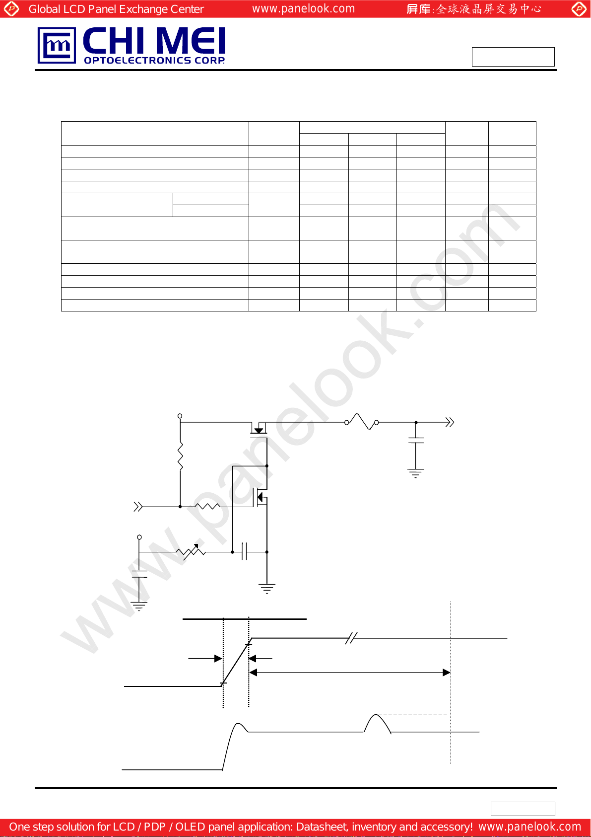
Measurement Conditions: Shown as the following figure. Test pattern: black.
+3.3V
R1
47K
Q1 2SK1475
FUSE
C3
1uF
(High to Low)
(Control Signal)
SW
+12V
C1
1uF
VR1
R2
1K
47K
0.01uF
Q2
2SK1470
C2
Vcc rising time is 470us
0.9Vcc
0V
470us
0.1Vcc
+3.3V
100ms
I
I
RUSH
IS
Vcc
(LCD Module Input)
VCC
ICC
7 / 30
The information described in this technical specification is tentative and it is possible to be changed without prior
notice. Please contact CMO ’s representative while your product design is based on this specification.
Version 1.0
Page 8
Global LCD Panel Exchange Center
www.panelook.com
One step solution for LCD / PDP / OLED panel application: Datasheet, inventory and accessory!
www.panelook.com
|
)
)
Note (3) The specified power supply current is under the conditions at Vcc = 3.3 V, Ta = 25 ± 2 ºC, fv = 60
Hz, whereas a power dissipation check pattern belo w is displayed.
Doc No.:
Issued Date: Feb. 25, 2008
Model No.: N133I6 - L01
Preliminary
Note (4) The specified power are the sum of LCD panel electronics input power and the converter input
a. White Pattern
Active Area
power. Test conditions are as follows.
(a) Vcc = 3.3 V, Ta = 25 ± 2 ºC, f
(b) The pattern used is a black and white 32 x 36 checkerboard, slide #100 from the VESA file
“Flat Panel Display Monitor Setup Patterns”, FPDMSU.ppt.
(c) Luminance: 60 nits.
(d) CMO doesn’t provide the converter in this product.
= 60 Hz,
v
b. Black Pattern
Active Area
Note (5) The parameters of LVDS signals are defined as the following figures.
CM
Single Ended
Differential
V
0V
V
TH(LVDS
0V
V
TL(LVDS
VID|
|VID|
3.2 BACKLIGHT UNIT Ta = 25 ± 2 ºC
8 / 30
The information described in this technical specification is tentative and it is possible to be changed without prior
notice. Please contact CMO ’s representative while your product design is based on this specification.
Version 1.0
Page 9
Global LCD Panel Exchange Center
www.panelook.com
One step solution for LCD / PDP / OLED panel application: Datasheet, inventory and accessory!
www.panelook.com
Doc No.:
Issued Date: Feb. 25, 2008
Model No.: N133I6 - L01
Preliminary
Parameter Symbol
LED Quantity 54 PCs (1)
LED Light Bar Power
Supply Voltage
LED Light Bar Power
Supply Current
Power Consumption PL -- 3.46 -- W (3), (Duty 100%)
LED Life Time LBL 10000 -- -- Hrs (4)
Note (1) LED light bar configuration is shown as below.
Note (2) For better LED light bar driving quality, it is recommended to utilize the adaptive boost converter with current
balancing function to drive LED light-bar.
Light Bar Feedback
Channels
27 28.8 30.6 V
V
L
-- 120 -- mA
I
L
Min. Typ. Max.
V
L, IL
Value
LED
Light Bar
Parallel:6
Series:9
Unit Note
(1),(2) (Duty 100%)
Note (3) P
Note (4) The lifetime of LED is defined as the time when it continues to operate under the co nditions at Ta = 25 ±2
= IL ×VL
L
and I
= 20 mA(Per EA) until the brightness becomes ≦ 50% of its original value.
L
o
C
9 / 30
The information described in this technical specification is tentative and it is possible to be changed without prior
notice. Please contact CMO ’s representative while your product design is based on this specification.
Version 1.0
Page 10

Global LCD Panel Exchange Center
www.panelook.com
One step solution for LCD / PDP / OLED panel application: Datasheet, inventory and accessory!
www.panelook.com
4. BLOCK DIAGRAM
4.1 TFT LCD MODULE
Doc No.:
Issued Date: Feb. 25, 2008
Model No.: N133I6 - L01
Preliminary
LVDS Display
Data & Clock
Vcc
GND
Data
CLK
EDID
V
LED Power & Signal
EDID
EDID
LVDS INPUT /
TIMING CONTROLLER
INPUT CONNECTOR
DC/DC CONVERTER &
REFERENCE VOLTAGE
GENERATOR
EDID
EEPROM
SCAN DRIVER IC
TFT LCD PANEL
DA TA DRIVER IC
BACKLIGHT UNIT
10 / 30
The information described in this technical specification is tentative and it is possible to be changed without prior
notice. Please contact CMO ’s representative while your product design is based on this specification.
Version 1.0
Page 11

Global LCD Panel Exchange Center
www.panelook.com
One step solution for LCD / PDP / OLED panel application: Datasheet, inventory and accessory!
www.panelook.com
5. INPUT TERMINAL PIN ASSIGNMENT
5.1 TFT LCD MODULE
Pin Symbol Description Polarity Remark
1 Vss Ground
2 Vcc Power Supply +3.3 V (typical)
3 Vcc Power Supply +3.3 V (typical)
4 V
5 NC No connect
6 CLK
7 DATA
8 Rxin0- LVDS Differential Data Input Negative
9 Rxin0+ LVDS Differential Data Input Positive
10 Vss Ground
11 Rxin1- LVDS Differential Data Input Negative
12 Rxin1+ LVDS Differential Data Input Positive
13 Vss Ground
14 Rxin2- LVDS Differential Data Input Negative B2~B5, DE, Hsync, Vsync
15 Rxin2+ LVDS Differential Data Input Positive
16 Vss Ground
17 CLK- LVDS Clock Data Input Negative
18 CLK+ LVDS Clock Data Input Positive
19 Vss Ground
20 Vss Ground
21 Vdc(1&2&3) LED Annold (Positive)
22 Vdc(4&5&6) LED Annold (Positive)
23 NC No connect
24 Vdc1 LED Cathode (Negative)
25 Vdc2 LED Cathode (Negative)
26 Vdc3 LED Cathode (Negative)
27 Vdc4 LED Cathode (Negative)
28 Vdc5 LED Cathode (Negative)
29 Vdc6 LED Cathode (Negative)
30 Vss Ground
Note (1) Connector Part No.: 20347-330E-12(I-PEX) or equivalent
DDC 3.3V Power DDC 3.3V Power
EDID
DDC Clock DDC Clock
EDID
DDC Data DDC Data
EDID
Doc No.:
Issued Date: Feb. 25, 2008
Model No.: N133I6 - L01
Preliminary
R0~R5,G0
-
G1~G5, B0, B1
-
LVDS Level Clock
Note (2) User’s connector Part No: 20345-030T-12(I-PEX) or equivalent
11 / 30
The information described in this technical specification is tentative and it is possible to be changed without prior
notice. Please contact CMO ’s representative while your product design is based on this specification.
Version 1.0
Page 12

Global LCD Panel Exchange Center
www.panelook.com
One step solution for LCD / PDP / OLED panel application: Datasheet, inventory and accessory!
www.panelook.com
5.3 TIMING DIAGRAM OF LVDS INPUT SIGNAL
Doc No.:
Issued Date: Feb. 25, 2008
Model No.: N133I6 - L01
Preliminary
CLK+
Rxin2
Rxin1
Rxin0
T/7
IN20 IN19 IN18 IN17 IN16 IN15 IN14
DE B5 B4 B3 B2 Vsync Hsync
IN13 IN12 IN11 IN10 IN9 IN8 IN7
B1 G4 G3 G2 G1 B0 G5
IN6 IN5 IN4 IN3 IN2 IN1 IN0
G0 R3 R2 R1 R0 R5 R4
Signal for 1 DCLK Cycle (T)
12 / 30
The information described in this technical specification is tentative and it is possible to be changed without prior
notice. Please contact CMO ’s representative while your product design is based on this specification.
Version 1.0
Page 13

Global LCD Panel Exchange Center
www.panelook.com
One step solution for LCD / PDP / OLED panel application: Datasheet, inventory and accessory!
www.panelook.com
5.4 COLOR DATA INPUT ASSIGNMENT
The brightness of each primary color (red, green and blue) is based on the 6-bit gray scale data input for
the color. The higher the binary input, the brighter the color. The table below provides the assignment of
color versus data input.
Color
R5 R4 R3 R2 R1 R0 G5 G4 G3 G2 G1 G0 B5 B4 B3 B2 B1 B0
Black
Red
Green
Basic
Colors
Gray
Scale
Of
Red
Gray
Scale
Of
Green
Gray
Scale
Of
Blue
Note (1) 0: Low Level Volt age, 1: High Level Voltage
Blue
Cyan
Magenta
Yellow
White
Red(0)/Dark
Red(1)
Red(2)
:
:
Red(61)
Red(62)
Red(63)
Green(0)/Dark
Green(1)
Green(2)
:
:
Green(61)
Green(62)
Green(63)
Blue(0)/Dark
Blue(1)
Blue(2)
:
:
Blue(61)
Blue(62)
Blue(63)
0
0
1
1
0
0
0
0
0
0
1
1
1
1
1
1
0
0
0
0
0
0
:
:
1
1
1
1
1
1
0
0
0
0
0
0
:
:
0
0
0
0
0
0
0
0
0
0
0
0
:
:
0
0
0
0
0
0
Doc No.:
Issued Date: Feb. 25, 2008
Model No.: N133I6 - L01
Preliminary
Data Signal
Red Green Blue
0
0
0
0
0
0
0
0
0
0
0
0
0
0
0
0
1
1
1
1
0
0
0
0
0
0
0
0
0
0
0
0
0
0
0
0
1
1
1
1
1
1
0
0
0
0
0
0
0
0
0
0
0
0
0
0
0
0
1
1
1
1
1
1
0
0
0
0
1
1
1
1
1
1
1
1
1
1
1
1
1
1
1
1
0
0
0
0
0
0
1
1
1
1
1
1
1
1
1
1
1
1
1
1
1
1
0
0
0
0
0
0
1
1
1
1
1
1
1
1
1
1
1
1
1
1
1
1
0
0
0
0
0
0
0
0
0
0
0
0
0
0
0
0
0
0
0
1
0
0
0
0
0
0
0
0
0
0
0
0
0
0
1
0
0
0
0
0
0
0
0
0
0
0
0
0
:
:
:
:
:
:
:
:
:
:
:
:
:
:
:
:
:
:
:
:
:
:
:
:
:
:
:
:
:
:
:
:
:
:
1
1
0
1
0
0
0
0
0
0
0
0
0
0
0
0
1
1
1
0
0
0
0
0
0
0
0
0
0
0
0
0
1
1
1
1
0
0
0
0
0
0
0
0
0
0
0
0
0
0
0
0
0
0
0
0
0
0
0
0
0
0
0
0
0
0
0
0
0
0
0
0
0
1
0
0
0
0
0
0
0
0
0
0
0
0
0
0
1
0
0
0
0
0
0
0
:
:
:
:
:
:
:
:
:
:
:
:
:
:
:
:
:
:
:
:
:
:
:
:
:
:
:
:
:
:
:
:
:
:
0
0
0
0
1
1
1
1
0
1
0
0
0
0
0
0
0
0
0
0
1
1
1
1
1
0
0
0
0
0
0
0
0
0
0
0
1
1
1
1
1
1
0
0
0
0
0
0
0
0
0
0
0
0
0
0
0
0
0
0
0
0
0
0
0
0
0
0
0
0
0
0
0
0
0
0
0
0
0
1
0
0
0
0
0
0
0
0
0
0
0
0
0
0
1
0
:
:
:
:
:
:
:
:
:
:
:
:
:
:
:
:
:
:
:
:
:
:
:
:
:
:
:
:
:
:
:
:
:
:
0
0
0
0
0
0
0
0
0
0
1
1
1
1
0
1
0
0
0
0
0
0
0
0
0
0
1
1
1
1
1
0
0
0
0
0
0
0
0
0
0
0
1
1
1
1
1
1
13 / 30
The information described in this technical specification is tentative and it is possible to be changed without prior
notice. Please contact CMO ’s representative while your product design is based on this specification.
Version 1.0
Page 14

Global LCD Panel Exchange Center
www.panelook.com
One step solution for LCD / PDP / OLED panel application: Datasheet, inventory and accessory!
www.panelook.com
Doc No.:
Issued Date: Feb. 25, 2008
Model No.: N133I6 - L01
Preliminary
5.5 EDID DATA STRUCTURE
The EDID (Extended Display Identification Data) data formats are to support displays as defined in the VESA Plug &
Display and FPDI standards.
Byte #
(decimal)
0
1
2
3
4
5
6
7
8
9
10
11
12
13
14
15
16
17
18
19
20
21
22
23
24
25
26
27
28
29
30
31
32
33
34
35
36
37
38
39
40
41
Byte #
(hex)
Field Name and Comments
0 Header
1 Header
2 Header
3 Header
4 Header
5 Header
6 Header
7 Header
8 EISA ID manufacturer name (“APP”)
9 EISA ID manufacturer name (Compressed AS CII)
0A ID product code (N133I6-L01) 6F
0B ID product code (hex LSB first; N133I6-L01) 9C
0C ID S/N (fixed “0”)
0D ID S/N (fixed “0”)
0E ID S/N (fixed “0”)
0F ID S/N (fixed “0”)
10 Week of manufacture (fixed “35”)
11 Year of manufacture (fixed “2007”)
12 EDID structure version # (“1”)
13 EDID revision # (“3”)
14 Video I/P definition (“digital”)
15 Max H image size (“29.7cm”)
16 Max V image size (“19.2cm”)
17 Display Gamma (Gamma = ”2.2”)
18 Feature support (“Active off, RGB Color”)
19 Red/Green (Rx1, Rx0, Ry1, Ry0, Gx1, Gx0, Gy1, Gy0)
1A Blue/White (Bx1, Bx0, By1, By0, Wx1, Wx0, Wy1, Wy0)
1B Red-x (Rx = “0.595”)
1C Red-y (Ry = “0.345”) 58
1D Green-x (Gx = ”0.320”)
1E Green-y (Gy = ”0.555”)
1F Blue-x (Bx = ”0.155”)
20 Blue-y (By = ”0.145”)
21 White-x (Wx = ”0.313”)
22 White-y (Wy = ”0.329”)
23 Established timings 1
24 Established timings 2 (1280x800@60Hz)
25 Manufacturer’s reserved timings
26 Standard timing ID # 1
27 Standard timing ID # 1
28 Standard timing ID # 2
29 Standard timing ID # 2
Value
(hex)
00 00000000
FF 11111111
FF 11111111
FF 11111111
FF 11111111
FF 11111111
FF 11111111
00 00000000
06 00000110
10 00010000
00 00000000
00 00000000
00 00000000
00 00000000
23 00100011
11 00010001
01 00000001
03 00000011
80 10000000
1D 00011101
13 00010011
78 01111000
0A 00001010
5C 01011100
80 10000000
98 10011000
51 01010001
8E 10001110
27 00100111
25 00100101
50 01010000
54 01010100
00 00000000
00 00000000
00 00000000
01 00000001
01 00000001
01 00000001
01 00000001
Value
(binary)
01101111
10011100
01011000
14 / 30
The information described in this technical specification is tentative and it is possible to be changed without prior
notice. Please contact CMO ’s representative while your product design is based on this specification.
Version 1.0
Page 15

Global LCD Panel Exchange Center
www.panelook.com
One step solution for LCD / PDP / OLED panel application: Datasheet, inventory and accessory!
www.panelook.com
Doc No.:
Issued Date: Feb. 25, 2008
Model No.: N133I6 - L01
Preliminary
42
43
44
45
46
47
48
49
50
51
52
53
54
55
56
57
58
59
60
61
62
63
64
65
66
67
68
69
70
71
72
73
74
75
76
77
78
79
80
81
82
83
84
85
86
2A Standard timing ID # 3
2B Standard timing ID # 3
2C Standard timing ID # 4
2D Standard timing ID # 4
2E Standard timing ID # 5
2F Standard timing ID # 5
30 Standard timing ID # 6
31 Standard timing ID # 6
32 Standard timing ID # 7
33 Standard timing ID # 7
34 Standard timing ID # 8
35 Standard timing ID # 8
Detailed timing description # 1 Pixel clock (“72.5MHz”,
36
According to VESA CVT Rev1.1)
37 # 1 Pixel clock (hex LSB first)
38 # 1 H active (“1280”)
39 # 1 H blank (“160”)
3A # 1 H active : H blank (“1280 : 160”)
3B # 1 V active (”800”)
3C # 1 V blank (”23”)
3D # 1 V active : V blank (”800 :23”)
3E # 1 H sync offset (”48”)
3F # 1 H sync pulse width ("32”)
40 # 1 V sync offset : V sync pulse width (”3 : 6”)
# 1 H sync offset : H sync pulse width : V sync offset : V sync
41
width (”48: 32 : 3 : 6”)
42 # 1 H image size (”286.08 mm”)
43 # 1 V image size (”178.8 mm”)
44 # 1 H image size : V image size (”286 : 178”)
45 # 1 H boarder (”0”)
46 # 1 V boarder (”0”)
# 1 Non-interlaced, Normal, no stereo, Separate sync, H/V pol
47
Negatives
48 Detailed timing/monitor
49 descriptor #2
4A
4B
4C Version
4D Apple edid signature
4E Apple edid signature
4F Link Type (LVDS Link,MSB justified)
50 Pixel and link component format (6-bit panel interface)
51 Panel features (No converter)
52
53
54
55
56
01 00000001
01 00000001
01 00000001
01 00000001
01 00000001
01 00000001
01 00000001
01 00000001
01 00000001
01 00000001
01 00000001
01 00000001
52 01010010
1C 00011100
00 00000000
A0 10100000
50 01010000
20 00100000
17 00010111
30 00110000
30 00110000
20 00100000
36 00110110
00 00000000
1E 00011110
B2 10110010
10 00010000
00 00000000
00 00000000
18 00011000
00 00000000
00 00000000
00 00000000
01 00000001
00 00000000
06 00000110
10 00010000
20 00100000
00 00000000
00 00000000
00 00000000
00 00000000
00 00000000
00 00000000
00 00000000
15 / 30
The information described in this technical specification is tentative and it is possible to be changed without prior
notice. Please contact CMO ’s representative while your product design is based on this specification.
Version 1.0
Page 16

Global LCD Panel Exchange Center
www.panelook.com
One step solution for LCD / PDP / OLED panel application: Datasheet, inventory and accessory!
www.panelook.com
Doc No.:
Issued Date: Feb. 25, 2008
Model No.: N133I6 - L01
Preliminary
87
88
89
90
91
92
93
94
95
96
97
98
99
100
101
102
103
104
105
106
107
108
109
110
111
112
113
114
115
116
117
118
119
120
121
122
123
124
125
126
127
57
58
59
5A Detailed timing description # 3
5B # 3 Flag
5C # 3 Reserved
# 3 FE (hex) defines ASCII string (Mod el Name “N133I3-L01”,
5D
ASCII)
5E # 3 Flag
5F # 3 1st character of name (“N”)
60 # 3 2nd character of name (“1”)
61 # 3 3rd character of name (“3”)
62 # 3 4th character of name (“3”)
63 # 3 5th character of name (“I”)
64 # 3 6th character of name (“6”)
65 # 3 7th character of name (“-”)
66 # 3 8th character of name (“L”)
67 # 3 9th character of name (“0”)
68 # 3 9th character of name (“1”)
69 # 3 New line character indicates end of ASCII string
6A # 3 Padding with “Blank” character
6B # 3 Padding with “Blank” character
6C Detailed timing description # 4
6D # 4 Flag
6E # 4 Reserved
6F # 4 FC (hex) defines Monitor name ("Color LCD", ASCII)
70 # 4 Flag
71 # 4 1st character of name ("C") 43
72 # 4 2nd character of name ("o") 6F
73 # 4 3rd character of name ("l") 6C
74 # 4 4th character of name ("o") 6F
75 # 4 5th character of name ("r") 72
76 # 4 6th character of name (<space>) 20
77 # 4 7th character of name ("L") 4C
78 # 4 8th character of name ("C") 43
79 # 4 9th character of name ("D")
7A # 4 New line character # 4 indicates e nd of Monitor name
7B # 4 Padding with "Blank" character
7C # 4 Padding with "Blank" character
7D # 4 Padding with "Blank" character
7E Extension flag
7F Checksum
00 00000000
0A 00001010
20 00100000
00 00000000
00 00000000
00 00000000
FE 11111110
00 00000000
4E 01001110
31 00110001
33 00110011
33 00110011
49 01001001
36 00110110
2D 00101101
4C 01001100
30 00110000
31 00110001
0A 00001010
20 00100000
20 00100000
00 00000000
00 00000000
00 00000000
FC 11111100
00 00000000
01000011
01101111
01101100
01101111
01110010
00100000
01001100
01000011
44 01000100
0A 00001010
20 00100000
20 00100000
20 00100000
00 00000000
4E 01001110
16 / 30
The information described in this technical specification is tentative and it is possible to be changed without prior
notice. Please contact CMO ’s representative while your product design is based on this specification.
Version 1.0
Page 17

Global LCD Panel Exchange Center
www.panelook.com
One step solution for LCD / PDP / OLED panel application: Datasheet, inventory and accessory!
www.panelook.com
5.5 EDID SIGINAL SPECIFICATION
(1) EDID Power
Parameter Symbol Test Condition Min. Typ. Max. Unit
Power supply
voltage
Vcc — 1.8 — 5.5 V
Doc No.:
Issued Date: Feb. 25, 2008
Model No.: N133I6 - L01
Preliminary
(2) DC characteristics
Parameter Symbol Test Condition Min Typ Max Unit
Supply current Vcc=5.0V Icc READ at 100kHz — 0.4 1.0 mA
Supply current Vcc=5.0V Icc WRITE at 100kHz — 2.0 3.0 mA
Standby Current ISB Vin=Vcc or Vss — 1.6 4.0 µA
Input Leakage Current ILI Vin=Vcc or Vss — 0.1 3.0 µA
Onput Leakage Current ILO Vout=Vcc or Vss — 0.05 3.0 µA
Input Low Level VIL — -0.6 — Vcc x 0.3 V
Input High Level VIH — Vcc x 0.7 — Vcc+0.5 V
Output Low Level Vcc=3.0V VOL2 IOL=2.1mA — — 0.4 V
Output Low Level Vcc=1.8V VOL1 IOL=0.15mA — — 0.2 V
17 / 30
The information described in this technical specification is tentative and it is possible to be changed without prior
notice. Please contact CMO ’s representative while your product design is based on this specification.
Version 1.0
Page 18

Global LCD Panel Exchange Center
www.panelook.com
One step solution for LCD / PDP / OLED panel application: Datasheet, inventory and accessory!
www.panelook.com
(3) AC char acteristics (VCC=1.8~5.5V standard operation mode)
Parameter Symbol Min Max Unit
Clock Frequency, SCL FSCL — 400 kHz
Doc No.:
Issued Date: Feb. 25, 2008
Model No.: N133I6 - L01
Preliminary
Clock Pulse Width Low TLOW 1.2 —
Clock Pulse Width High THIGH 0.6 —
Noise Suppression Time TI — 50 ns
Clock Low to Data Out Valid TAA 0.1 0.9
Time the bus must be free
BUF 1.2 —
before a new transmission
can start
Start Hold Time THD.STA 0.6 —
Start Set-up Time TSU.STA 0.6 —
Data in Hold Time THD.DAT 0 —
Data in Set-up Time TSU.DAT 100 — ns
Inputs Rise Ti me TR — 0.3
T
μs
μs
μs
μs
μs
μs
μs
μs
Inputs Fall Time TF — 300 ns
Stop Set-up Time TSU.STO 0.6 —
Data Out Hold Time TDH 50 — ns
Write Cycle T ime TWR — 5 ms
μs
18 / 30
The information described in this technical specification is tentative and it is possible to be changed without prior
notice. Please contact CMO ’s representative while your product design is based on this specification.
Version 1.0
Page 19

Global LCD Panel Exchange Center
www.panelook.com
One step solution for LCD / PDP / OLED panel application: Datasheet, inventory and accessory!
www.panelook.com
6. INTERFACE TIMING
6.1 INPUT SIGNAL TIMING SPECIFICATIONS
The specifications of input signal timing are as the following table and timing diagram.
Signal Item Symbol Min. Typ. Max. Unit Note
DCLK Frequency 1/Tc 50 71 80 MHz -
Vertical Total Time TV 810 823 1900 TH -
DE
Note (1) Because this module is operated by DE only mode, Hsync and Vsync are ignored.
Vertical Addressing Time TVD 800 800 800 TH -
Horizontal Total Time TH 1360 1440 1900 Tc -
Horizontal Addressing Time THD 1280 1280 1280 T c -
Doc No.:
Issued Date: Feb. 25, 2008
Model No.: N133I6 - L01
Preliminary
INPUT SIGNAL TIMING DIAGRAM
DE
DCLK
TC
DE
DATA
HD
T
19 / 30
The information described in this technical specification is tentative and it is possible to be changed without prior
notice. Please contact CMO ’s representative while your product design is based on this specification.
Version 1.0
Page 20

Global LCD Panel Exchange Center
www.panelook.com
One step solution for LCD / PDP / OLED panel application: Datasheet, inventory and accessory!
www.panelook.com
6.2 POWER ON/OFF SEQUENCE
Power On
Power Off
Doc No.:
Issued Date: Feb. 25, 2008
Model No.: N133I6 - L01
Preliminary
Restart
Power Supply
for LCD, Vcc
0V
- L VDS Interface
0V
- Power for Lamp
Timing Specifications:
0.5 ≦ t1 ≦ 10 ms
0 ≦ t2 ≦ 50 ms
0 ≦ t3 ≦ 50 ms
t4 ≧ 500 ms
t5 ≧ 200 ms
10%
90%
t1
90%
Valid Data
t6 t5
50%50%
ONOFF OFF
t7
10%
t4
t3 t2
10%
t6 ≧ 200 ms
Note (1) Please follow the power on/off sequence described above. Otherwise, the LCD module might be
damaged.
Note (2) Please avoid floating state of interface signal at invalid period. When the interface signal is invalid, be
sure to pull down the power supply of LCD Vcc to 0 V.
Note (3) The Backlight converter power must be turned on after the power supply for the logic and the
interface signal is valid. The Backlight converter power must be turned off before the power supply
for the logic and the interface signal is invalid.
Note (4) Sometimes some slight noise shows when LCD is turned off (even backlight is already off). To
avoid this phenomenon, we suggest that the Vcc falling time is better to follow
5≦t7≦300 ms.
20 / 30
The information described in this technical specification is tentative and it is possible to be changed without prior
notice. Please contact CMO ’s representative while your product design is based on this specification.
Version 1.0
Page 21

Global LCD Panel Exchange Center
www.panelook.com
One step solution for LCD / PDP / OLED panel application: Datasheet, inventory and accessory!
www.panelook.com
7 OPTICAL CHARACTERISTICS
7.1 TEST CONDITIONS
Item Symbol Value Unit
Ambient Temperature Ta 25±2
Ambient Humidity Ha 50±10 %RH
Supply Voltage VCC 3.3 V
Input Signal According to typical value in "3. ELECTRICAL CHARACTERISTICS"
LED Light Bar Input Current IL
The measurement methods of optical characteristics are shown in Section 7.2. The following items
should be measured under the test conditions described in Section 7.1 and stable environment shown in
Note (5).
7.2 OPTICAL SPECIFICATIONS
Item Symbol Condition Min. Typ. Max. Unit Note
Contrast Ratio CR 300 400 - (2), (5)
Response Time
Center Luminance of White Lct 338 413 cd/m2(4), (5)
Luminance Uniformity U 60 % (5), (8)
Red
Color
Chromaticity
Cross-talk
Color Difference w.r.t. center - - 0.009 - (5), (9)
Color Difference over panel - - 0.013 - (5), (10)
Color Difference worst neighbor
Viewing Angle
Green
Blue
White
Horizontal
Vertical
Doc No.:
Issued Date: Feb. 25, 2008
Model No.: N133I6 - L01
Preliminary
o
C
120
TR - 5 10 ms
- 11 16 ms
T
F
Rx 0.575
0.600
0.625 Ry 0.325 0.345 0.365 Gx 0.300 0.320 0.340 -
θ
=0°, θY =0°
Gy 0.535 0.555 0.575 Bx 0.130 0.150 0.170 By 0.090 0.120 0.150 -
x
Viewing Normal
Angle
Wx 0.290 0.306 0.322 Wy 0.311 0.327 0.343 -
D
SHA
- - 4 % (5), (6)
- - 0.005 - (5), (11)
θ
+
x
θ
-
x
θ
+
Y
-
θ
Y
CR≥10
60 70
60 70
50 60
55 65
mA
(3)
(5)
Deg. (1)
21 / 30
The information described in this technical specification is tentative and it is possible to be changed without prior
notice. Please contact CMO ’s representative while your product design is based on this specification.
Version 1.0
Page 22

Global LCD Panel Exchange Center
www.panelook.com
One step solution for LCD / PDP / OLED panel application: Datasheet, inventory and accessory!
www.panelook.com
.67 ms
Note (1) Definition of Viewing Angle (θx, θy):
Doc No.:
Issued Date: Feb. 25, 2008
Model No.: N133I6 - L01
Preliminary
θX- = 90º
x-
6 o’clock
θ
y- = 90º
y-
Note (2) Definition of Contrast Ratio (CR):
The contrast ratio can be calculated by the following expression.
Contrast Ratio (CR) = L
L
: Luminance of gray level 63
63
L
: Luminance of gray level 0
0
63
/ L0
Normal
θx = θy = 0º
θy- θy+
θx−
θx+
y+
12 o’clock direction
θ
y+ = 90º
x+
θX+ = 90º
CR = CR (5)
CR (X) is corresponding to the Contrast Ratio of the point X at Figure in Note (7).
Note (3) Definition of Response Time (T
100%
90%
Optical
Response
10%
0%
T
R
66.67 ms
, TF):
R
66
Time
T
F
22 / 30
The information described in this technical specification is tentative and it is possible to be changed without prior
notice. Please contact CMO ’s representative while your product design is based on this specification.
Version 1.0
Page 23

Global LCD Panel Exchange Center
www.panelook.com
One step solution for LCD / PDP / OLED panel application: Datasheet, inventory and accessory!
www.panelook.com
500
A
A
y
Note (4) Definition of Center Luminance of White (Lct):
Doc No.:
Issued Date: Feb. 25, 2008
Model No.: N133I6 - L01
Preliminary
Measure the luminance of gray level 63 at center points
Lct = L (5)
L (x) is corresponding to the luminance of the point X at Figure in Note (7 ).
Note (5) Measurement Setup:
The LCD module should be stabilized at given temperature for 15 minutes to avoid abrupt
temperature change during measuring. In order to stabilize the luminance, the measurement
should be executed after lighting Backlight for 15 minutes in a windless room.
LCD Module
LCD Panel
USB2000
CS-1000T
Note (6) Definition of Cross-talk (D
D
= | YB – YA | / YA ×100 (%)
SHA
Where:
Y
= Luminance of measured location without gray level 0 pattern (cd/m2)
A
Y
= Luminance of measured location with gray level 0 pattern (cd/m2)
B
(0, 0)
Y
(D/8,W/2)
A, L
Gray 32
Y
(D/2,7W/8)
A, D
Center of the Screen
mm
)
SHA
ctive Area
Y
(D/2,W/8)
A, U
Y
(7D/8,W/2)
A, R
(D,W)
(D/4,W/4)
Y
(D/8,W/2)
B, L
Y
(D/2,7W/8)
B, D
Light Shield Room
(Ambient Luminance < 2 lux)
(0, 0)
ctive Area
Gray 0
Gra
32
Y
B, U
Y
B, R
(3D/4,3W/4)
(D,W)
(D/2,W/8)
(7D/8,W/2)
23 / 30
The information described in this technical specification is tentative and it is possible to be changed without prior
notice. Please contact CMO ’s representative while your product design is based on this specification.
Version 1.0
Page 24

Global LCD Panel Exchange Center
www.panelook.com
One step solution for LCD / PDP / OLED panel application: Datasheet, inventory and accessory!
www.panelook.com
Note (7) Definition of measure point
Doc No.:
Issued Date: Feb. 25, 2008
Model No.: N133I6 - L01
Preliminary
W/4
W/2
W
Ve rtical Line
3W/4
Note (8) Definition of Luminance Uniformity(U)
U = Lmin/Lmax
Where:
Lmax = max {Luminance values at 160 points},
Lmin = min {Luminance values at 160 points}
Horizontal Line
D
D/4 D/2 3D/4
12
X
: Test Point
X=1 to 5
3
5
4
Active Area
0 1/17L 16/ 17L L
0
1/11W
10W/11
1
W
Note (9) Definition of Color Difference with respect to the center
Center color coordinate is defined as the Average of points of 72, 73, 88, 89. where
is corresponding to the measured point in Note (8)
Color Difference = [(u’
- u’c) 2 +(v’x - v’c) 2]
x
1/2
Where x is any point in Note (8) , c is the center point.
Note (10) Definition of Color Difference over the p anel
Color Difference between any two measured p oints over the 160 points
- u’y) 2 +(v’x - v’y) 2]
=[(u’
x
1/2
Where x , y is any two points in Note (8)
Note (11) Definition of Color Difference between two neighbor
Color Difference between any two neighboring points on the panel
- u’y) 2 +(v’x - v’y) 2]
=[(u’
x
1/2
Where x , y is any two neighbor points in Note (8)
16
160
24 / 30
The information described in this technical specification is tentative and it is possible to be changed without prior
notice. Please contact CMO ’s representative while your product design is based on this specification.
Version 1.0
Page 25

Global LCD Panel Exchange Center
www.panelook.com
One step solution for LCD / PDP / OLED panel application: Datasheet, inventory and accessory!
www.panelook.com
Doc No.:
Issued Date: Feb. 25, 2008
Model No.: N133I6 - L01
Preliminary
8. PRECAUTIONS
8.1 ASSEMBL Y AND HANDLING PRECAUTIONS
(1) Do not apply rough force such as bending or twisting to the module during assembly.
(2) To assemble or install module into user’s system can be only in clean working areas. The dust and oil
may cause electrical short or worsen the polarizer.
(3) It’s not permitted to have pressure or impulse on the module because the LCD panel and Backlight will
be damaged.
(4) Always follow the correct power sequence when LCD module is connecting and operating. This can
prevent damage to the CMOS LSI chips during latch-up.
(5) Do not pull the I/F connector in or out while the module is operating.
(6) Do not disassemble the module.
(7) Use a soft dry cloth without chemicals for cleaning, because the surface of polarizer is very soft and
easily scratched.
(8) It is dangerous that moisture come into or contacted the LCD module, because moisture may damage
LCD module when it is operating.
(9) High temperature or humidity may reduce the performance of module. Please store LCD module within
the specified storage conditions.
(10) When ambient temperature is lower than 10ºC may reduce the display quality. For example, the
response time will become slowly, and the starting voltage of CCFL will be higher than room
temperature.
8.2 SAFETY PRECAUTIONS
(1) The startup voltage of Backlight is approximately 1000 Volts. It may cause electrical shock while
assembling with converter . Do not disassemble the module or insert anything into the Backlight unit.
(2) If the liquid crystal material leaks from the panel, it should be kept away from the eyes or mouth. In
case of contact with hands, skin or clothes, it has to be washe d away thoroughly with soap.
(3) After the module’s end of life, it is not harmful in case of normal operation and storage.
8.3 OPERATION PRECAUTIONS
(1) Do not pull the I/F connector in or out while the module is operating.
(2) Always follow the correct power on/off sequence when LCD module is connecting and operating. This
can prevent the CMOS LSI chips from damage during latch-up.
(3) The startup voltage of Backlight is approximately 1000 Volts. It may cause electrical shock while
assembling with converter . Do not disassemble the module or insert anything into the Backlight unit.
25 / 30
The information described in this technical specification is tentative and it is possible to be changed without prior
notice. Please contact CMO ’s representative while your product design is based on this specification.
Version 1.0
Page 26

Global LCD Panel Exchange Center
www.panelook.com
One step solution for LCD / PDP / OLED panel application: Datasheet, inventory and accessory!
www.panelook.com
9. PACKAGING
9.1 CARTON
Doc No.:
Issued Date: Feb. 25, 2008
Model No.: N133I6 - L01
Preliminary
Figure. 9-1 Packing method
26 / 30
The information described in this technical specification is tentative and it is possible to be changed without prior
notice. Please contact CMO ’s representative while your product design is based on this specification.
Version 1.0
Page 27

Global LCD Panel Exchange Center
www.panelook.com
One step solution for LCD / PDP / OLED panel application: Datasheet, inventory and accessory!
www.panelook.com
9.2 PALLET
Doc No.:
Issued Date: Feb. 25, 2008
Model No.: N133I6 - L01
Preliminary
Figure. 9-2 Packing method
27 / 30
The information described in this technical specification is tentative and it is possible to be changed without prior
notice. Please contact CMO ’s representative while your product design is based on this specification.
Version 1.0
Page 28

Global LCD Panel Exchange Center
www.panelook.com
One step solution for LCD / PDP / OLED panel application: Datasheet, inventory and accessory!
www.panelook.com
10. DEFINITION OF LABELS
10.1 CMO MODULE LABEL
The barcode nameplate is pasted on each module as illustration, and its definitions are as following
explanation.
(a) Model Name: N133I6 - L01
(b) Revision: Rev. XX, for example: A1, …, C1, C2 …etc.
Doc No.:
Issued Date: Feb. 25, 2008
Model No.: N133I6 - L01
Preliminary
(c) Serial ID: X X
(d) Production Location: MADE IN XXXX. XXXX stands for production location.
Serial ID includes the information as below:
(a) Manufactured Date: Year: 1~9, for 2001~2009
(b) Revision Code: cover all the change
(c) Serial No.: Manufacturing sequence of product
X X X X X Y M D X N N N N
Month: 1~9, A~C, for Jan. ~ De c.
Day: 1~9, A~Y, for 1
st
Serial No.
CMO Internal Use
Year, Month, Date
CMO Internal Use
Revision
CMO Internal Use
to 31st, exclude I , O and U
28 / 30
The information described in this technical specification is tentative and it is possible to be changed without prior
notice. Please contact CMO ’s representative while your product design is based on this specification.
Version 1.0
Page 29

Global LCD Panel Exchange Center
www.panelook.com
One step solution for LCD / PDP / OLED panel application: Datasheet, inventory and accessory!
www.panelook.com
10.2 CMO CARTON LABEL
Doc No.:
Issued Date: Feb. 25, 2008
Model No.: N133I6 - L01
Preliminary
29 / 30
The information described in this technical specification is tentative and it is possible to be changed without prior
notice. Please contact CMO ’s representative while your product design is based on this specification.
Version 1.0
Page 30

Global LCD Panel Exchange Center
www.panelook.com
One step solution for LCD / PDP / OLED panel application: Datasheet, inventory and accessory!
www.panelook.com
 Loading...