

Page 1
Global LCD Panel Exchange Center
www.panelook.com
Global LCD Panel Exchange Center
www.panelook.com
Page 2
Global LCD Panel Exchange Center
www.panelook.com
- - CONTENTS -
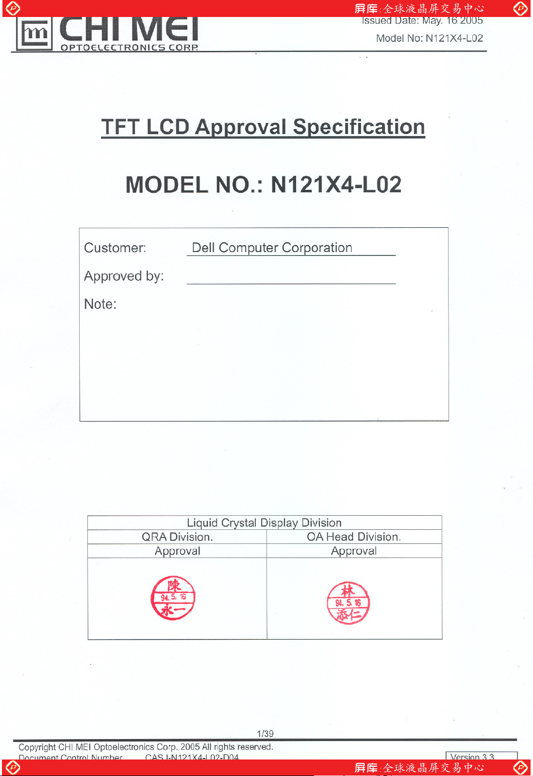
Issued Date: May. 16 2005
Model No: N121X4-L02
1. Handling Precautions ............................................................................................................................. 4
2. General Description................................................................................................................................5
2.1 Product Summary ............................................................................................................................... 6
2.2 Functional Block Diagram ................................................................................................................... 7
3. Absolute Maximum Ratings.................................................................................................................... 8
4. Pixel Format Image ................................................................................................................................9
5. Mechanical Characteristics................................................................................................................... 10
6. Optical Characteristics...........................................................................................................................11
6.1 Optical Characteristics .......................................................................................................................11
6.2 Luminance Uniformity ....................................................................................................................... 13
7. Electrical Characteristics ...................................................................................................................... 14
7.1 Interface Connector .......................................................................................................................... 14
7.2 LVDS Receiver.................................................................................................................................. 16
7.3 Interface Timings............................................................................................................................... 20
7.4 EEDID............................................................................................................................................... 21
7.5 Power Consumption.......................................................................................................................... 26
7.6 Power ON/OFF Sequence ................................................................................................................ 27
7.7 BIST.................................................................................................................................................. 28
8. Inverter ................................................................................................................................................. 30
8.1 Interface Connector .......................................................................................................................... 30
8.2 Electrical Characteristics................................................................................................................... 31
9. Qualifications and CFL Life................................................................................................................... 33
9.1 Visual Screen Quality........................................................................................................................ 33
9.2 Line Defect........................................................................................................................................ 33
9.3 Bright and Black Dots ....................................................................................................................... 34
9.4 CFL Life ............................................................................................................................................ 34
10. Packaging Specifications...................................................................................................................... 35
11. Labels................................................................................................................................................... 37
11.1 Serial Number Label ......................................................................................................................... 37
11.2 Date Label ........................................................................................................................................ 37
11.3 PPID Label........................................................................................................................................ 38
11.4 UL Label............................................................................................................................................ 38
12. Appendix .............................................................................................................................................. 39
12.1 National Test Lab Requirement ..................................................................................................... 39
12.2 Conditions of Acceptability............................................................................................................. 39
2/39
Copyright CHI MEI Optoelectronics Corp. 2005 All rights reserved.
Document Control Number CAS I-N121X4-L02-D04 Version 3.3
One step solution for LCD / PDP / OLED panel application: Datasheet, inventory and accessory!
www.panelook.com
Page 3
Global LCD Panel Exchange Center
www.panelook.com
Issued Date: May. 16 2005
Model No: N121X4-L02
REVISION HISTORY
Date Document Revision Page Summary
March 24, 2004 OEM I-N121X4-L02 All First Edition for customer.
July 7, 2004 OEM I-N121X4-L02-02 Second edition
Oct. 6, 2004 OEM I-N121X4-L02-03 Page 6
Page 11
Oct. 25, 2004 OEM I-N121X4-L02-04 Page 10 5Mechanical Characteristics: mounting hole position 2.8mm -> 2.5mm
Nov.11, 2004 CAS-I-N121X4-L02-D01 Page 13
Page 28
Page 21
Page 33
Page 35
Page 37
Dec. 6, 2004 CAS-I-N121X4-L02-D02 Page 4
Page 6
Page 11
2.1Product Summary: fixed typo: Storage temp –20 to 60degC
6Optical Characteristics: Color chromaticity changed
Added 6.2 Luminance Uniformity
Added 7.7BIST
Added 7.4EEDID
Added 9Qualifications and CFL Life
Added 10Packaging
Added 11Labels
1 Handling Precautions: UL 1950 => UL 60950
Table 1 Product summary: B/L power consumption 4.6W max => 4.4W max
6.1 Optical Characteristics: Viewing angle 40 typ => 40 min, etc.
Page 11
Page 20
Page 21
Page 27
Page 30
Page 31
Page 31
Page 32
Page 39
Mar. 8, 2005 CAS-I-N121X4-L02-D03 Page 7
Page 10
Page 21
Page 30
Page 36
May. 16, 2005 CAS-I-N121X4-L02-D04 Page 38 11.3 PPID Label; Corrected REV code (A00 => A02)
6.1 Optical Characteristics: White luminance 120 min => 127 min
7.3.1 Timing Characteristics: changed V-total time min 777 => 780
7.4 EEDID: Revision X02 data
7.6 Power ON/OFF Sequence: VESA style symbols
8.1 Interface Connector: Added description of LAMP_STAT pin
Table 19 Electrical Specifications: Input power changed(4.6W max=-> 4.4W
max), P(5VSUS) 25mW max => 70mW max, P(5VALW) 10mW max => 10mW
max
8.2 Electrical Characteristics: Removed dimming table
Figure 16 SMData – Luminance: Updated.
12 Appendix Fixed typo: UL 60960 => UL 90950, SELF => SELV
2.2 Functional Block Diagram: Added BISTEN to block diagram
5 Mechanical Characteristics: Corrected label position in reference drawing
7.4 EEDID: Corrected BIST Enable Flag(7Ah) 0 => 1
8.1 Interface Connector: Corrected part number(lead-free type)
10 Packaging Specifications: Added packaging type (B)
3/39
Copyright CHI MEI Optoelectronics Corp. 2005 All rights reserved.
Document Control Number CAS I-N121X4-L02-D04 Version 3.3
One step solution for LCD / PDP / OLED panel application: Datasheet, inventory and accessory!
www.panelook.com
Page 4
Global LCD Panel Exchange Center
www.panelook.com
Issued Date: May. 16 2005
Model No: N121X4-L02
1. Handling Precautions
z If any signals or power lines deviate from the power on/off sequence, it may cause shorten the life of the LCD module.
z The LCD panel and the CFL are made of glass and may break or crack if dropped on a hard surface, so please handle
them with care.
z CMOS ICs are included in the LCD panel. They should be handled with care, to prevent electrostatic discharge.
z Do not press the reflector sheet at the LCD module to any directions.
z Do not stick the adhesive tape on the reflector sheet at the back of the LCD module.
z Please handle with care when mount in the system cover. Mechanical damage for lamp cable/lamp connector may
cause safety problems.
z Small amount of materials having no flammability grade is used in the LCD module. The LCD module should be supplied
by power complied with requirements of Limited Power Source (2.11, IEC60950 or UL60950), or be applied exemption
conditions of flammability requirements (4.4.3.3, IEC60950 or UL60950) in an end product.
z The LCD module is designed so that the CFL in it is supplied by Limited Current Circuit (2.4, IEC60950 or UL60950).
z The fluorescent lamp in the liquid crystal display (LCD) contains mercury. Do not put it in trash that is disposed of in
landfills. Dispose of it as required by local ordinances or regulations.
z Never apply detergent or other liquid directly to the screen.
z Wipe off water drop immediately. Long contact with water may cause discoloration or spots.
z When the panel surface is soiled, wipe it with absorbent cotton or other soft cloth; do not use solvents or abrasives.
z Do not touch the front screen surface in your system, even bezel.
z Gently wipe the covers and the screen with a soft cloth.
z The information contained herein is presented only as a guide for the applications of our products. No
responsibility is assumed by CHI MEI Optoelectronics for any infringements of patents or other right of the
third partied which may result from its use. No license is granted by implication or otherwise under any patent
or patent rights of CHI MEI Optoelectronics or others.
4/39
Copyright CHI MEI Optoelectronics Corp. 2005 All rights reserved.
Document Control Number CAS I-N121X4-L02-D04 Version 3.3
One step solution for LCD / PDP / OLED panel application: Datasheet, inventory and accessory!
www.panelook.com
Page 5

Global LCD Panel Exchange Center
www.panelook.com
Issued Date: May. 16 2005
Model No: N121X4-L02
2. General Description
z This specification applies to 12.1 inch Color TFT/LCD Module 'N121X4-L02'.
z This module is designed for a display unit of notebook style personal computer.
z The screen format and electrical interface are intended to support the XGA (1024(H) x768 (V)) screen.
z This module contains an inverter card for backlight.
z BIST (Built-In Self Test) function
z VESA CVT reduced blanking mode support
z Compliant with RoHS (Restriction of the Use of Certain Hazardous Substances) directive
5/39
Copyright CHI MEI Optoelectronics Corp. 2005 All rights reserved.
Document Control Number CAS I-N121X4-L02-D04 Version 3.3
One step solution for LCD / PDP / OLED panel application: Datasheet, inventory and accessory!
www.panelook.com
Page 6
Global LCD Panel Exchange Center
www.panelook.com
Issued Date: May. 16 2005
Model No: N121X4-L02
2.1 Product Summary
Table 1 shows the summary of this LCD module. Unless otherwise noted, all characteristics are at 25 degree C
condition.
Table 1 Product summary
ITEMS SPECIFICATIONS
Screen Diagonal [mm] 307.2
Active Area [mm] 245.76(H) x 184.32(V)
Pixels H x V 1024(x3) x 768
Pixel Pitch [mm] 0.240(per one triad) x 0.240
Pixel Arrangement R.G.B. Vertical Stripe
Display Mode Normally White
White Luminance [cd/m2] 150 typ. (5 Points average, SMData=00H)
Contrast Ratio 300: 1 Typ.
Optical Rise Time + Fall Time [msec] 50Max.
Nominal Input Voltage[Volt]
VDD
5VSUS, 5VALW line
PWR_SRC line
Logic Power Consumption [watt](VDD Line) 0.9 Typ. (All Black Pattern)
Backlight Power Consumption [watt] 4.4 Max(SMData=00H)
Weight [grams] 280 Typ, 295 max. (with inverter)
Physical Size [mm] 261.0(W) x 209.5(H) x 4.7(D) Typ. (with Inverter space)
Electrical Interface (Logic) Single LVDS(4 pairs LVDS)
Electrical Interface (Inverter) SMB_CLK, SMB_DAT, FPVEE, LAMP_STAT
Support Color Native 262K colors (RGB 6-bit data driver)
Temperature Range (degree C)
Operating
+3.3 Typ
+5.0 Typ
+14.4 Typ.
261.0(W) x 198.0(H) x 4.7(D) Typ. (without inverter space)
EEDID (clock, data)
BISTEN
0 to +50
Storage (Shipping)
-20 to +60
6/39
Copyright CHI MEI Optoelectronics Corp. 2005 All rights reserved.
Document Control Number CAS I-N121X4-L02-D04 Version 3.3
One step solution for LCD / PDP / OLED panel application: Datasheet, inventory and accessory!
www.panelook.com
Page 7
Global LCD Panel Exchange Center
www.panelook.com
2.2 Functional Block Diagram
Figure 1 shows the functional block of the color TFT/LCD Module:
Figure 1 Block Diagram
TFT LCD Module
LCD Drive Card
VDD
GND
BISTEN
4 pairs s ingle
channel LVDS
RxIN0+/RxIN1+/RxIN2+/RxCLKIN+/-
Signal Connector DF19L-20P-1H
Timing Controller LSI
DC/DC converter
Referenc e
voltage circ uit
Issued Date: May. 16 2005
Model No: N121X4-L02
X-Driver
Y-Driver
TFT Array/Cell
1024(R/G/B) x 768
VEEDID
ClkEDID
DataEDID
PWR_SRC
GND
5VSUS
5VALW
SMB_DAT
SMB_CLK
FPVEE
LAMP_STAT
Connector LVC-
D20SYFG3
EEDID EEPROM
Inverter
AMP 1565747-2
Backlight Unit
Lamp Connector
JST BHSR-02VS-1
7/39
Copyright CHI MEI Optoelectronics Corp. 2005 All rights reserved.
Document Control Number CAS I-N121X4-L02-D04 Version 3.3
One step solution for LCD / PDP / OLED panel application: Datasheet, inventory and accessory!
www.panelook.com
Page 8
Global LCD Panel Exchange Center
www.panelook.com
Issued Date: May. 16 2005
Model No: N121X4-L02
3. Absolute Maximum Ratings
Table 2 Absolute maximum ratings
Item Symbol Min Max Unit Conditions
Supply Voltage
Input Voltage of Signal
VDD -0.3 +4.0 V
5VSUS
5VALW
PWR_SRC -0.3 +25 V
Logic input
signals(LVDS,
EDID, BISTEN)
FPVEE -0.3 5.5 V
SMB_CLK
SMB_DAT
-0.3 +5.5 V
-0.3 VDD+0.3 V
-1.0 7.0 V
Operating Temperature TOP 0 +50 deg. C (Note)
Operating Humidity HOP 8 95 %RH (Note)
Storage Temperature TST -20 +60 deg. C (Note)
Storage Humidity HST 5 95 %RH (Note)
Vibration 1.5 10-200 G Hz
Shock 50 18 G ms Rectangle Wave
Note: Maximum Wet-Bulb should be 39 degree C and No condensation.
8/39
Copyright CHI MEI Optoelectronics Corp. 2005 All rights reserved.
Document Control Number CAS I-N121X4-L02-D04 Version 3.3
One step solution for LCD / PDP / OLED panel application: Datasheet, inventory and accessory!
www.panelook.com
Page 9
Global LCD Panel Exchange Center
www.panelook.com
4. Pixel Format Image
Figure 2 shows the relationship of the input signals and LCD pixel format image.
Figure 2 Pixel Format
0
1
R
G
B
G
R
1st Line
BR
Issued Date: May. 16 2005
Model No: N121X4-L02
1022 1023
G
G
B
BR
768th Line
B
R
R
G
B
G
RG
B
G
B
R
9/39
Copyright CHI MEI Optoelectronics Corp. 2005 All rights reserved.
Document Control Number CAS I-N121X4-L02-D04 Version 3.3
One step solution for LCD / PDP / OLED panel application: Datasheet, inventory and accessory!
www.panelook.com
Page 10
Global LCD Panel Exchange Center
www.panelook.com
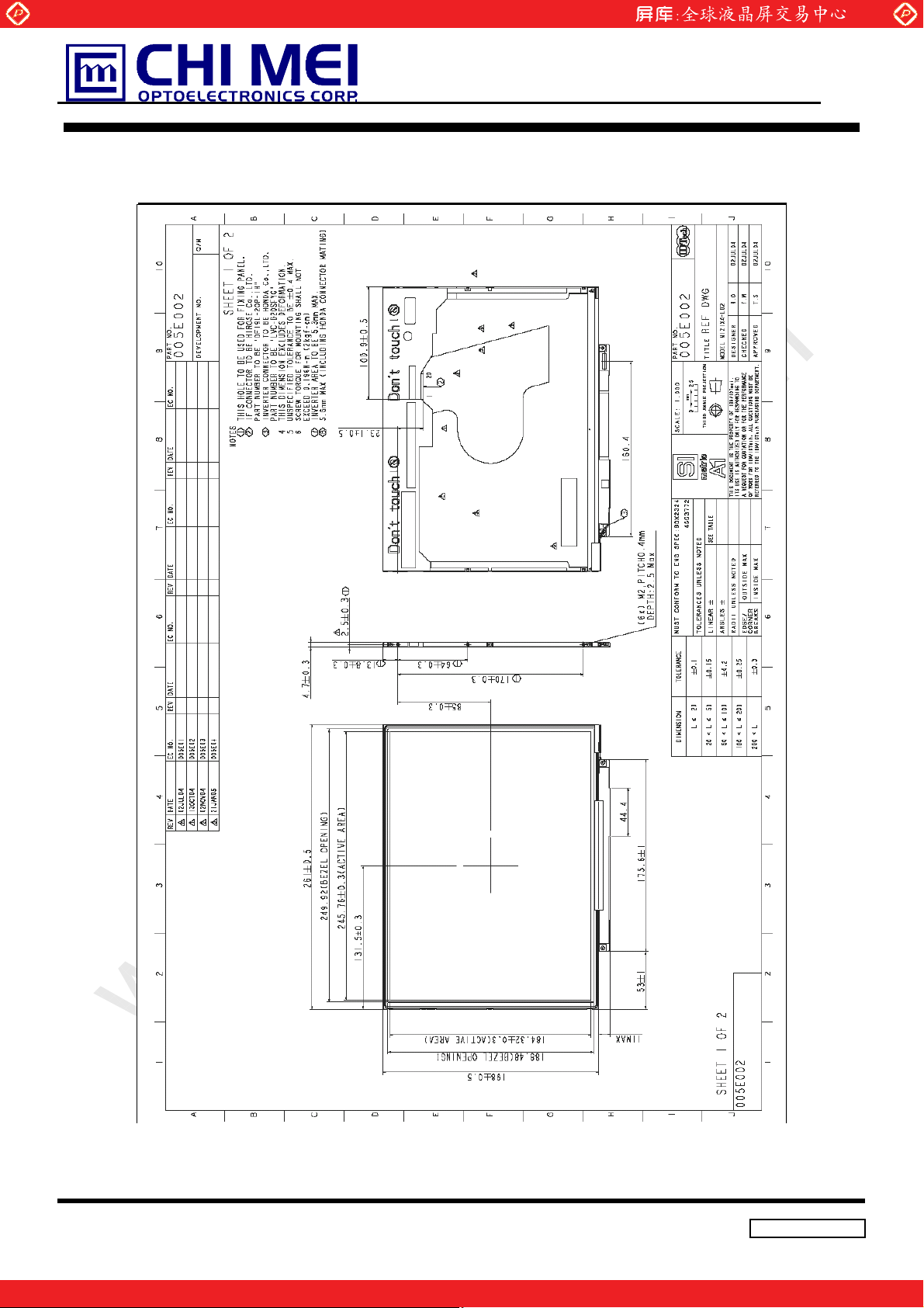
5. Mechanical Characteristics
Figure 3 Reference outline drawing
Issued Date: May. 16 2005
Model No: N121X4-L02
10/39
Copyright CHI MEI Optoelectronics Corp. 2005 All rights reserved.
Document Control Number CAS I-N121X4-L02-D04 Version 3.3
One step solution for LCD / PDP / OLED panel application: Datasheet, inventory and accessory!
www.panelook.com
Page 11
Global LCD Panel Exchange Center
www.panelook.com
Issued Date: May. 16 2005
Model No: N121X4-L02
6. Optical Characteristics
6.1 Optical Characteristics
The optical characteristics are measured under stable conditions as follows under 25 degree C condition:
Table 3 Optical characteristics
Specification Item Conditions
Min Typ. Max Note
Viewing Angle (Degrees) Horizontal (Right)
K>10(Left)
K: Contrast Ratio Vertical (Upper)
K>10 (Lower)
Contrast ratio 230 300 -
Response Time(ms) Rising + Falling - - 50
Color Chromaticity(CIE)
White Luminance(cd/m2) 5 Points average
Red x 0.558 0.584 0.610 +/-0.026
Red y 0.308 0.336 0.364 +/-0.028
Green x 0.296 0.322 0.348 +/-0.026
Green y 0.506 0.534 0.562 +/-0.028
Blue x 0.125 0.151 0.177 +/-0.026
Blue y 0.100 0.128 0.156 +/-0.028
White x 0.287 0.313 0.339 +/-0.026
White y 0.301 0.329 0.357 +/-0.028
SMData=00H
40
40
15
30
127 150
-
-
-
-
-
-
-
-
11/39
Copyright CHI MEI Optoelectronics Corp. 2005 All rights reserved.
Document Control Number CAS I-N121X4-L02-D04 Version 3.3
One step solution for LCD / PDP / OLED panel application: Datasheet, inventory and accessory!
www.panelook.com
Page 12
Global LCD Panel Exchange Center
www.panelook.com
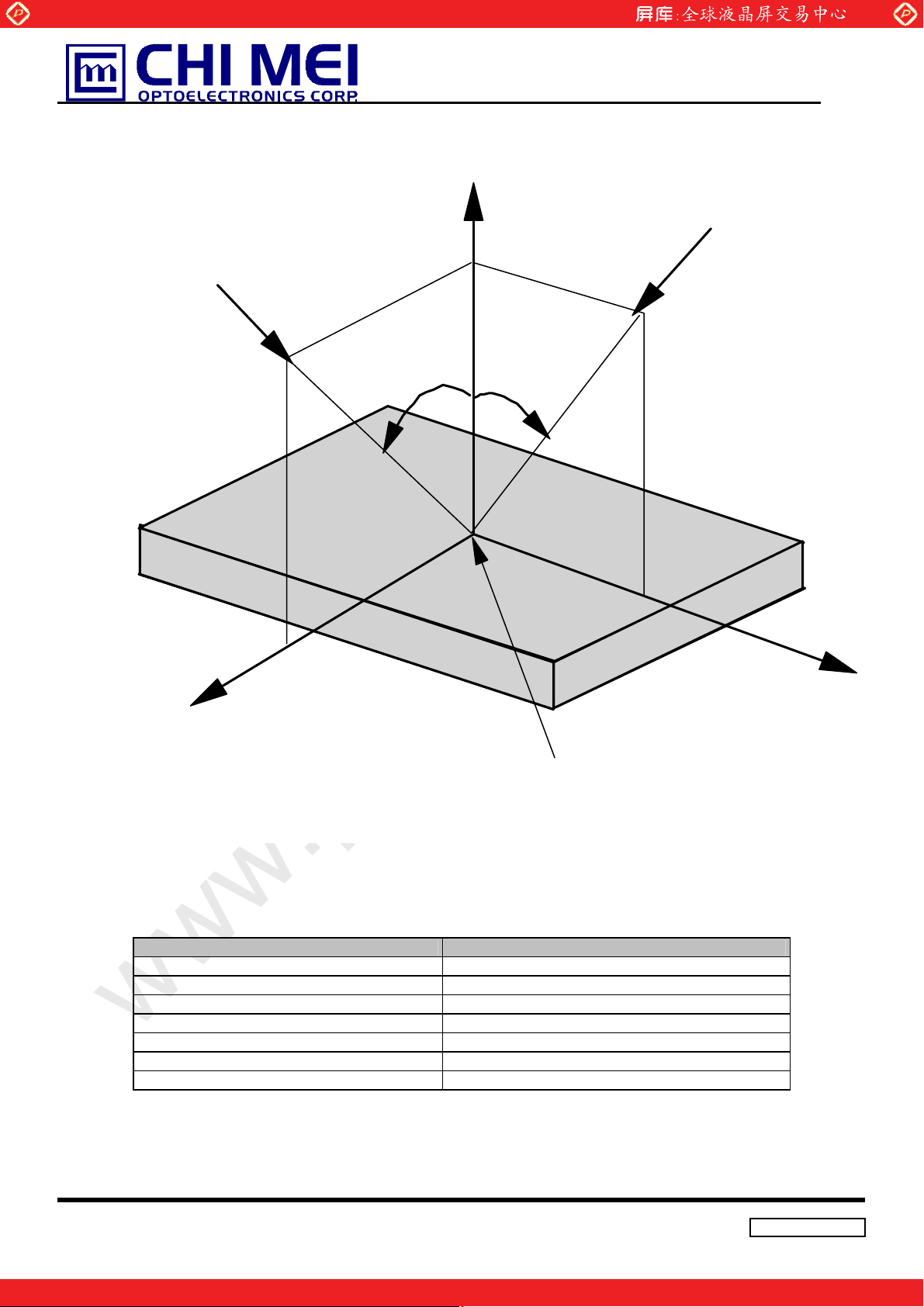
Figure 4 Note for the Optical Characteristics
Issued Date: May. 16 2005
Model No: N121X4-L02
Z
Viewing or Measuring
Direction
Viewing or Measuring
Direction
+h-v
LEFT
UPPER
LOWER
RIGHT
X
CENTER OF LCD
(X=0,Y=0,Z=0)
z Chromaticity and White Balance are defined as the C.I.E. 1931 x,y coordinates at the center of LCD. The Standard
Equipments are as shown below table.
Table 4 Standard Equipments
Item Standard Equipment
Viewing Angle MCPD-7000 by Ohtsuka Elec.
Contrast MCPD-7000 by Ohtsuka Elec.
Response Time BM5A by TOPCON OPTICAL Co.,Ltd.
White Luminance MCPD-7000 by Ohtsuka Elec.
Luminance Uniformity MCPD-7000 by Ohtsuka Elec.
Chromaticity MCPD-7000 by Ohtsuka Elec.
White Balance MCPD-7000 by Ohtsuka Elec.
The measurement is to be done after 30 minutes of Power-on of Backlight.
Unless otherwise specified, the ambient conditions are as following.
Y
12/39
Copyright CHI MEI Optoelectronics Corp. 2005 All rights reserved.
Document Control Number CAS I-N121X4-L02-D04 Version 3.3
One step solution for LCD / PDP / OLED panel application: Datasheet, inventory and accessory!
www.panelook.com
Page 13

Global LCD Panel Exchange Center
www.panelook.com
Issued Date: May. 16 2005
Model No: N121X4-L02
Table 5 Ambient conditions
Ambient Temperature 25 +/-2 (deg C)
Ambient Humidity 25 to 85 (%)
Atmospheric Pressure 86.0 to 104.0 ( kPa )
6.2 Luminance Uniformity
When backlight is on with all pixels in the unselected state(white raster), average luminance and luminance
uniformity(variation) is defined as below.
54321
LLLLL
LuminanceAverage
5
)5,2,1max(
LLL
UNF(5pts) d
UNF(13pts) d
LLL
LLL
LLL
25.1
)5,2,1min(
)13,2,1max(
65.1
)13,2,1min(
Figure 5 Average luminance and Luminance uniformity test points
L6 L7
L9
L11
10mm
L1 L2
L5
L3
L12 L13
256
512
768
L8
L10
L4
10mm
10mm
192
384
576
10mm
13/39
Copyright CHI MEI Optoelectronics Corp. 2005 All rights reserved.
Document Control Number CAS I-N121X4-L02-D04 Version 3.3
One step solution for LCD / PDP / OLED panel application: Datasheet, inventory and accessory!
www.panelook.com
Page 14

Global LCD Panel Exchange Center
www.panelook.com
Issued Date: May. 16 2005
Model No: N121X4-L02
7. Electrical Characteristics
7.1 Interface Connector
Table 6 Connector Name / Designation
Manufacturer HIROSE
Type / Part Number DF19L-20P-1H
Mating Receptacle/Part Number DF19G-20S-1F (FPC Type)
DF19G-20S-1C (Cable Type)
Table 7 Signal pin assignment
Pin # Signal Name Description Remarks
1 GND Ground
2 VDD
3 VDD
+3.3V Power Supply
4 VEDID EEDID 3.3V Power Supply Power source shall be the limited current
circuit that has not exceeding 1A. Refer to
"Enhanced Display Data Channel (E-DDCTM)
Proposed Standard", VESA.
5 BISTEN BIST(Built-In Self Test) enable L: Normal operation
H: BIST enable
See 7.7BIST for detail.
6 ClkEDID EEDID Clock
7 DataEDID (Note 2, 4) EEDID Data
8 RxIN0-
9 RxIN0+
10 GND Ground
11 R x IN1 -
12 RxIN1+
13 GND Ground
14 RxIN2-
15 RxIN2+
LVDS differential data input (Red0-Red5,
Green0)
LVDS differential data input (Green1-Green5,
Blue0-Blue1)
LVDS differential data input (Blue2-Blue5,
HSync, VSync, DSPTMG)
CLKEEDID line and DATAEEDID line are
pulled up with 10k ohm resistor to VEEDID
power source line at LCD panel, respectively.
Has 100ohm termination resistor
Has 100ohm termination resistor
Has 100ohm termination resistor
16 GND Ground
17 RxCLKIN-
18 RxCLKIN+
19 GND Ground
20 GND Ground
LVDS differential clock input Has 100ohm termination resistor
All input signals shall be low or Hi-Z state when VDD is off.
14/39
Copyright CHI MEI Optoelectronics Corp. 2005 All rights reserved.
Document Control Number CAS I-N121X4-L02-D04 Version 3.3
One step solution for LCD / PDP / OLED panel application: Datasheet, inventory and accessory!
www.panelook.com
Page 15

Global LCD Panel Exchange Center
www.panelook.com
Issued Date: May. 16 2005
Model No: N121X4-L02
Table 8 Interface Signal Descriptions
SIGNAL NAME Description
+RED5
+RED4
+RED3
+RED2
+RED1
+RED0
+GREEN 5
+GREEN 4
+GREEN 3
+GREEN 2
+GREEN 1
+GREEN 0
+BLUE 5
+BLUE 4
Red Data 5 (MSB)
Red Data 4
Red Data 3
Red Data 2
Red Data 1
Red Data 0 (LSB)
Green Data 5 (MSB)
Green Data 4
Green Data 3
Green Data 2
Green Data 1
Green Data 0 (LSB)
Blue Data 5 (MSB)
Blue Data 4
Red-pixel Data
Each red pixel's brightness data consists of these 6 bits pixel data.
Green-pixel Data
Each green pixel's brightness data consists of these 6 bits pixel data.
Blue-pixel Data
Each blue pixel's brightness data consists of these 6 bits pixel data.
+BLUE 3
+BLUE 2
+BLUE 1
+BLUE 0
-DTCLK Data Clock The typical frequency is 56MHz. The signal is used to strobe the pixel data.
DSPTMG Display Timing When the signal is high, the pixel data shall be valid to be displayed.
VSYNC Vertical Sync
HSYNC Horizontal Sync
Blue Data 3
Blue Data 2
Blue Data 1
Blue Data 0 (LSB)
15/39
Copyright CHI MEI Optoelectronics Corp. 2005 All rights reserved.
Document Control Number CAS I-N121X4-L02-D04 Version 3.3
One step solution for LCD / PDP / OLED panel application: Datasheet, inventory and accessory!
www.panelook.com
Page 16

Global LCD Panel Exchange Center
www.panelook.com
Issued Date: May. 16 2005
Model No: N121X4-L02
7.2 LVDS Receiver
7.2.1. Signal Electrical Characteristics for LVDS Receiver
The built-in LVDS receiver is compatible with ANSI/TIA/TIA-644 standard.
Table 9 LVDS Receiver Electrical Characteristics
Parameter Symbol Min Typ Max Unit Conditions
Differential Input High Threshold Vth +100 mV Vcm=+1.2V
Differential Input Low Threshold Vtl -100 mV Vcm=+1.2V
Magnitude Differential Input Voltage |Vid| 100 600 mV
Common Mode Voltage Vcm 1.0 1.2 1.4 V Vth - Vtl = 200mV
Common Mode Voltage Offset Vcm -50 +50 mV Vth - Vtl = 200mV
Note:
Input signals shall be low or Hi-Z state when VDD is off.
All electrical characteristics for LVDS signal are defined and shall be measured at the interface connector of
LCD.
Parameter Symbol min typ max unit
Input low voltage VIL 0 0.3VDD V
Input high voltage VIH 0.7VDD VDD V
Input leakage current IIZ -10 10 uA
Table 10 Timing Requirements
Parameter Symbol Min Typ Max Unit Conditions Note
Clock Frequency fc 50 56 67 MHz VESA XGA CVT reduced blanking
Cycle Time tc 14.93 17.86 20.00 ns
Data Setup Time Tsu 600 ps (See Figure 9)
Data Hold Time Thd 600 ps
Cycle-to-cycle jitter tCCJ -150 +150 ps fc = 56MHz
Cycle Modulation
Rate
tCJavg 20 ps/clk fc = 56MHz
fc = 56MHz
tCCJ < 50ps
Vth-Vtl = 200m
Vcm = 1.2V
Vcm = 0
Tsu=Thd=600ps
Tsu=Thd=600ps
(See Figure 9)
Jitter is the magnitude of the change in input
clock period.
tCJavg is maximum average cycle
modulation rate in peak-to-peak transition
within any 100-clock cycles. Figure 10 Cycle
Modulation Rate illustrates a case against
this requirement. This specification is
applied only if input clock peak jitter within
any 100-clock cycles is greater than 300ps.
Note:.All values are at VDD=3.3V, Ta=25 degree C.
Figure 6 Voltage Definitions
16/39
Copyright CHI MEI Optoelectronics Corp. 2005 All rights reserved.
Document Control Number CAS I-N121X4-L02-D04 Version 3.3
One step solution for LCD / PDP / OLED panel application: Datasheet, inventory and accessory!
www.panelook.com
Page 17

Global LCD Panel Exchange Center
www.panelook.com
Issued Date: May. 16 2005
Model No: N121X4-L02
Figure 7 Measurement System
Figure 8 Data mapping
17/39
Copyright CHI MEI Optoelectronics Corp. 2005 All rights reserved.
Document Control Number CAS I-N121X4-L02-D04 Version 3.3
One step solution for LCD / PDP / OLED panel application: Datasheet, inventory and accessory!
www.panelook.com
Page 18

Global LCD Panel Exchange Center
www.panelook.com
Issued Date: May. 16 2005
Model No: N121X4-L02
Figure 9 Timing Definition (detail A)
Note: Tsu and Thd are internal data sampling window of receiver. Trskm is the system skew margin; i.e., the sum
of cable skew, source clock jitter, and other inter-symbol interference, shall be less than Trskm.
18/39
Copyright CHI MEI Optoelectronics Corp. 2005 All rights reserved.
Document Control Number CAS I-N121X4-L02-D04 Version 3.3
One step solution for LCD / PDP / OLED panel application: Datasheet, inventory and accessory!
www.panelook.com
Page 19

Global LCD Panel Exchange Center
www.panelook.com
Issued Date: May. 16 2005
Model No: N121X4-L02
Figure 10 Cycle Modulation Rate
7.2.2. LVDS Receiver Internal Circuit
Figure 11 LVDS Receiver Internal Circuit shows the internal block diagram of the LVDS receiver. This LCD module
equips termination resistors for LVDS link.
19/39
Copyright CHI MEI Optoelectronics Corp. 2005 All rights reserved.
Document Control Number CAS I-N121X4-L02-D04 Version 3.3
One step solution for LCD / PDP / OLED panel application: Datasheet, inventory and accessory!
www.panelook.com
Page 20

Global LCD Panel Exchange Center
www.panelook.com
Issued Date: May. 16 2005
Model No: N121X4-L02
Figure 11 LVDS Receiver Internal Circuit
7.2.3. Recommended Guidelines for Motherboard PCB Design and Cable Selection
Following the suggestions below will help to achieve optimal results.
z Use controlled impedance media for LADS signals. They should have a matched differential impedance of 100 ohm.
z Match electrical lengths between traces to minimize signal skew.
z Isolate TEL signals from LADS signals.
z For cables, twisted pair, twin, or flex circuit with close coupled differential traces are recommended.
7.3 Interface Timings
VESA CVT reduced blanking timing is supported.
If timing signal is invalid, the LCD enters "self protection mode" and the screen becomes whole black. Once the
signal is back, it resumes normal operation.
7.3.1. Timing Characteristics
Table 11 Interface timings
Symbol Parameter MIN TYP MAX Unit Note
20/39
Copyright CHI MEI Optoelectronics Corp. 2005 All rights reserved.
Document Control Number CAS I-N121X4-L02-D04 Version 3.3
One step solution for LCD / PDP / OLED panel application: Datasheet, inventory and accessory!
www.panelook.com
Page 21

Global LCD Panel Exchange Center
www.panelook.com
Issued Date: May. 16 2005
Model No: N121X4-L02
fdck DTCLK Frequency 56.00 MHz See Table 10 Timing
Requirements
tck DTCLK cycle time 17.86 nsec
Htotal H total time 1170 1184 2047 tck
Hac H active time 1024 1024 1024 tck
Hsw H-Sync width 8 32 tck
Hbp H back porch 8 80 tck
32 <= Hsw + Hbp < 515 [tck].
Hfp H front porch 0 48 tck
Vtotal V total time 780 790 1023 tx
Vac V active time 768 768 768 tx
Vsync Frame rate 55 60 61 Hz
Vsw V-sync Width 1 4 tx
Vfp V-sync front porch 1 3 tx
Vbp V-sync back porch 11 15 63 tx Vbp should be static.
7.3.2. Timing Definition
Figure 12 Timing Definitions
HSYNC
Htotal
Hfp Hsw Hbp
DSPTMG
VSYNC
Vtotal
Vfp Vsw Vbp
DSPTMG
Vac
Vac
7.4 EEDID
Table 12 EEDID
Supported Standards VESA ENHANCED EXTENDED DISPLAY IDENTIFICATION
DATA STANDARD Release A, Revision 1" and supports "EEDID
version 1.3
EEPROM IC BR24L02F(ROHM) or equivalent
I2C Device Address A0/A1
Table 13 Data table
Address Category Description Data Remark
00h Header Header 00h Header, Fixed
21/39
Copyright CHI MEI Optoelectronics Corp. 2005 All rights reserved.
Document Control Number CAS I-N121X4-L02-D04 Version 3.3
One step solution for LCD / PDP / OLED panel application: Datasheet, inventory and accessory!
www.panelook.com
Page 22

Global LCD Panel Exchange Center
www.panelook.com
Issued Date: May. 16 2005
Model No: N121X4-L02
01h Header Header FFh Header, Fixed
02h Header Header FFh Header, Fixed
03h Header Header FFh Header, Fixed
04h Header Header FFh Header, Fixed
05h Header Header FFh Header, Fixed
06h Header Header FFh Header, Fixed
07h Header Header 00h Header, Fixed
EISA Manuf. Code LSB 3 character in compressed ASCII:
08h Vendor/Product Identification ID Manufacturer Name 0Dh
09h Vendor/Product Identification ID Manufacturer Name AFh
0Ah Vendor/Product Identification ID Product Code 02h Panel Supplier Reserved - Product code 12 02
0Bh Vendor/Product Identification ID Product Code 12h Panel Supplier Reserved - Product code 12 02
"CMO -> 0D AF
EISA Manuf. Code LSB 3 character in compressed ASCII:
"CMO -> 0D AF
0Ch Vendor/Product Identification ID Serial Number 00h Optional 32-bit serial no. Unused(00h)
0Dh Vendor/Product Identification ID Serial Number 00h Optional 32-bit serial no. Unused(00h)
0Eh Vendor/Product Identification ID Serial Number 00h Optional 32-bit serial no. Unused(00h)
0Fh Vendor/Product Identification ID Serial Number 00h Optional 32-bit serial no. Unused(00h)
10h Vendor/Product Identification Week of Manufacture 00h Week of manufacture 1 - 53 (unused: 00h)
11h Vendor/Product Identification Year of Manufacture 00h Year of manufacture year - 1990(unsed:00h)
12h EDID Structure Version/Revision Version # 01h Version=1
13h EDID Structure Version/Revision Revision # 03h Revision=3
14h Basic Display Parameters/Features Video Input Definition 80h Signal Level: Digital DFP 1.x: no
Horizontal active area, rounded to nearest centimeter.
15h Basic Display Parameters/Features Max. Horitonal Image Size 19h
16h Basic Display Parameters/Features Max. Vertical Image Size 12h
Display Transfer
17h Basic Display Parameters/Features
18h Basic Display Parameters/Features Feature Support 0Ah
Characteristics(Gamma)
24.576cm -> 19h
Vertical active area, rounded to nearest centimeter.
18.432cm -> 12h
gamma=2.2 (gamma * 100-100 = 2.2*100-100 = 120 =
78h)
78h
DPMS:no Active off:no Type:RGB-color sRGB:no
Preferred Timing Mode:yes GTF:no
19h Color Characteristics Red/Green(D1-D0 E7h Rx1 Rx0 Ry1 Ry0 Gx1 Gx0 Gy1 Gy0
1Ah Color Characteristics Blue/White(D1-D0) B5h Bx1 Bx0 By1 By0 Wx1 Wx0 Wy1 Wy0
1Bh Color Characteristics Red-x(D9-D2) 93h Rx=0.577
1Ch Color Characteristics Red-y(D9-D2) 56h Ry=0.338
1Dh Color Characteristics Green-x(D9-D2) 4Fh Gx=0.310
1Eh Color Characteristics Green-y(D9-D2) 8Dh Gy=0.554
1Fh Color Characteristics Blue-x(D9-D2) 28h Bx=0.158
22/39
Copyright CHI MEI Optoelectronics Corp. 2005 All rights reserved.
Document Control Number CAS I-N121X4-L02-D04 Version 3.3
One step solution for LCD / PDP / OLED panel application: Datasheet, inventory and accessory!
www.panelook.com
Page 23

Global LCD Panel Exchange Center
www.panelook.com
Issued Date: May. 16 2005
Model No: N121X4-L02
20h Color Characteristics Blue-y(D9-D2) 1Fh By=0.124
21h Color Characteristics White-x(D9-D2) 50h Wx=0.313
22h Color Characteristics White-y(D9-D2) 54h Wy=0.329
23h Established Timings Established Timings 1 00h Not supported
24h Established Timings Established Timings 2 00h Not supported
Manufacturer's Reserved
25h Established Timings
26h Standard Timing Identification Standard Timing Identification #101h (Established timing: Hactive / 8 - 31 = 1024/8-31)
27h Standard Timing Identification Standard Timing Identification #101h
28h Standard Timing Identification Standard Timing Identification #2 01h 01h: Blank
29h Standard Timing Identification Standard Timing Identification #2 01h 01h: Blank
2Ah Standard Timing Identification Standard Timing Identification #3 01h 01h: Blank
Timings
00h No manufacturer's specific timing
(Established timing: Image aspect ratio=4:3 Refresh
rate=60Hz)
2Bh Standard Timing Identification Standard Timing Identification #3 01h 01h: Blank
2Ch Standard Timing Identification Standard Timing Identification #4 01h 01h: Blank
2Dh Standard Timing Identification Standard Timing Identification #4 01h 01h: Blank
2Eh Standard Timing Identification Standard Timing Identification #5 01h 01h: Blank
2Fh Standard Timing Identification Standard Timing Identification #5 01h 01h: Blank
30h Standard Timing Identification Standard Timing Identification #6 01h 01h: Blank
31h Standard Timing Identification Standard Timing Identification #6 01h 01h: Blank
32h Standard Timing Identification Standard Timing Identification #7 01h 01h: Blank
33h Standard Timing Identification Standard Timing Identification #7 01h 01h: Blank
34h Standard Timing Identification Standard Timing Identification #8 01h 01h: Blank
35h Standard Timing Identification Standard Timing Identification #8 01h 01h: Blank
36h Detailed Timing Descriptions Detailed Timing Description #1 E0h Pixel clock/10000(D7-D0) 56MHz/10000 = 5600 = 15E0h
Pixel clock/10000(D15-D8) 56MHz/10000 = 5600 =
37h Detailed Timing Descriptions Detailed Timing Description #1 15h
38h Detailed Timing Descriptions Detailed Timing Description #1 00h HActive(D7-D0) = 1024 mod 256 = 00h
39h Detailed Timing Descriptions Detailed Timing Description #1 A0h HBlank(D7-D0) = 160 mod 256 = A0h
15E0h
HActive(D11-D8) : HBlank(D11-D8) = 1024/256 : 160/256
3Ah Detailed Timing Descriptions Detailed Timing Description #1 40h
3Bh Detailed Timing Descriptions Detailed Timing Description #1 00h VActive(D7-D0) = 768 mod 256
3Ch Detailed Timing Descriptions Detailed Timing Description #1 16h VBlank(D7-D0) = 22 mod 256 = 16h
3Dh Detailed Timing Descriptions Detailed Timing Description #1 30h
3Eh Detailed Timing Descriptions Detailed Timing Description #1 30h HSyncOffset(D7-D0) = HBorder+HFrontPorch = 48 = 30h
3Fh Detailed Timing Descriptions Detailed Timing Description #1 20h HSyncWidth(D7-D0) = 32 = 20h
= 40h
VActive(D11-D8) : VBlank(D11-D8) = 768/256 : 22 / 256 =
30h
23/39
Copyright CHI MEI Optoelectronics Corp. 2005 All rights reserved.
Document Control Number CAS I-N121X4-L02-D04 Version 3.3
One step solution for LCD / PDP / OLED panel application: Datasheet, inventory and accessory!
www.panelook.com
Page 24

Global LCD Panel Exchange Center
www.panelook.com
Issued Date: May. 16 2005
Model No: N121X4-L02
40h Detailed Timing Descriptions Detailed Timing Description #1 34h VSyncOffset(D3-D0) : VSyncWidth(D3-D0) = 3:4 = 34h
HSyncOffset(D9-D8) : HSyncWidth(D9-D8) :
VSyncOffset(D5-D4) : VSyncWidth(D5-D4) = 0:0:0:0 =
41h Detailed Timing Descriptions Detailed Timing Description #1 00h
42h Detailed Timing Descriptions Detailed Timing Description #1 F6h HImageSize(mm, D7-D0) = 245.76mm = F6h
43h Detailed Timing Descriptions Detailed Timing Description #1 B8h VImageSize(mm, D7-D0) = 184.32mm = B8h
44h Detailed Timing Descriptions Detailed Timing Description #1 00h HImageSize(D11-D8) : VImageSize(D11-D8)
45h Detailed Timing Descriptions Detailed Timing Description #1 00h HBorder=0(Zero for notebook LCD)
46h Detailed Timing Descriptions Detailed Timing Description #1 00h VBorder=0(Zero for notebook LCD)
47h Detailed Timing Descriptions Detailed Timing Description #1 18h
48h Detailed Timing Descriptions Detailed Timing Description #2 00h Timimg Descriptor #2 Alternate Panel Timing -- not used
49h Detailed Timing Descriptions Detailed Timing Description #2 00h
00h
Non-interlaced, Normal Display, Digital separate,
Negative V/H sync porality, no DE-only mode support
4Ah Detailed Timing Descriptions Detailed Timing Description #2 00h
4Bh Detailed Timing Descriptions Detailed Timing Description #2 00h
4Ch Detailed Timing Descriptions Detailed Timing Description #2 00h
4Dh Detailed Timing Descriptions Detailed Timing Description #2 00h
4Eh Detailed Timing Descriptions Detailed Timing Description #2 00h
4Fh Detailed Timing Descriptions Detailed Timing Description #2 00h
50h Detailed Timing Descriptions Detailed Timing Description #2 00h
51h Detailed Timing Descriptions Detailed Timing Description #2 00h
52h Detailed Timing Descriptions Detailed Timing Description #2 00h
53h Detailed Timing Descriptions Detailed Timing Description #2 00h
54h Detailed Timing Descriptions Detailed Timing Description #2 00h
55h Detailed Timing Descriptions Detailed Timing Description #2 00h
56h Detailed Timing Descriptions Detailed Timing Description #2 00h
57h Detailed Timing Descriptions Detailed Timing Description #2 00h
58h Detailed Timing Descriptions Detailed Timing Description #2 00h
59h Detailed Timing Descriptions Detailed Timing Description #2 00h
5Ah Detailed Timing Descriptions Detailed Timing Description #3 00h Header flag 00h
5Bh Detailed Timing Descriptions Detailed Timing Description #3 00h Header flag 00h
5Ch Detailed Timing Descriptions Detailed Timing Description #3 00h Header flag 00h
5Dh Detailed Timing Descriptions Detailed Timing Description #3 FEh Header Data type tag(Monitor) ASCII String FEh
5Eh Detailed Timing Descriptions Detailed Timing Description #3 00h Header flag 00h
5Fh Detailed Timing Descriptions Detailed Timing Description #3 55h Dell P/N 1st Character - "U"
60h Detailed Timing Descriptions Detailed Timing Description #3 35h Dell P/N 1st Character - "5"
61h Detailed Timing Descriptions Detailed Timing Description #3 31h Dell P/N 1st Character - "1"
24/39
Copyright CHI MEI Optoelectronics Corp. 2005 All rights reserved.
Document Control Number CAS I-N121X4-L02-D04 Version 3.3
One step solution for LCD / PDP / OLED panel application: Datasheet, inventory and accessory!
www.panelook.com
Page 25

Global LCD Panel Exchange Center
www.panelook.com
Issued Date: May. 16 2005
Model No: N121X4-L02
62h Detailed Timing Descriptions Detailed Timing Description #3 32h Dell P/N 1st Character - "2"
63h Detailed Timing Descriptions Detailed Timing Description #3 32h Dell P/N 1st Character - "2"
64h Detailed Timing Descriptions Detailed Timing Description #3 03h LCD Supplier EEDID Revision #: X02 -> 03h
65h Detailed Timing Descriptions Detailed Timing Description #3 4Eh Manufacturer model name "N121X4" - "N"
66h Detailed Timing Descriptions Detailed Timing Description #3 31h Manufacturer model name "N121X4" - "1"
67h Detailed Timing Descriptions Detailed Timing Description #3 32h Manufacturer model name "N121X4" - "2"
68h Detailed Timing Descriptions Detailed Timing Description #3 31h Manufacturer model name "N121X4" - "1"
69h Detailed Timing Descriptions Detailed Timing Description #3 58h Manufacturer model name "N121X4" - "X"
6Ah Detailed Timing Descriptions Detailed Timing Description #3 34h Manufacturer model name "N121X4" - "4"
Empty: 20h(if <13 char, terminate with 0Ah, remaining
6Bh Detailed Timing Descriptions Detailed Timing Description #3 0Ah
6Ch Detailed Timing Descriptions Detailed Timing Description #4 00h Flag: 00h when block used as monitor descriptor
6Dh Detailed Timing Descriptions Detailed Timing Description #4 00h Flag: 00h when block used as monitor descriptor
char =20h)
6Eh Detailed Timing Descriptions Detailed Timing Description #4 00h Reserved: 00h when block used as monitor descriptor
6Fh Detailed Timing Descriptions Detailed Timing Description #4 FEh Data tag: FEh(ASCII string)
70h Detailed Timing Descriptions Detailed Timing Description #4 00h Flag: 00h when block used as descriptor
71h Detailed Timing Descriptions Detailed Timing Description #4 E5h SMBUS value @10[cd/m2] = E5h
72h Detailed Timing Descriptions Detailed Timing Description #4 D1h SMBUS value @17[cd/m2] = D1h
73h Detailed Timing Descriptions Detailed Timing Description #4 C3h SMBUS value @24[cd/m2] = C3h
74h Detailed Timing Descriptions Detailed Timing Description #4 BAh SMBUS value @30[cd/m2] = BAh
75h Detailed Timing Descriptions Detailed Timing Description #4 91h SMBUS value @60[cd/m2] = 91h
76h Detailed Timing Descriptions Detailed Timing Description #4 6Ch SMBUS value @90[cd/m2] = 6Ch
77h Detailed Timing Descriptions Detailed Timing Description #4 44h SMBUS value @120[cd/m2] = 44h
78h Detailed Timing Descriptions Detailed Timing Description #4 00h SMBUS value @150[cd/m2] = 00h
79h Detailed Timing Descriptions Detailed Timing Description #4 01h Number of LVDS receiver chip = 1
7Ah Detailed Timing Descriptions Detailed Timing Description #4 01 BIST Enable: Yes=01h
7Bh Detailed Timing Descriptions Detailed Timing Description #4 0Ah Terminator 0Ah
7Ch Detailed Timing Descriptions Detailed Timing Description #4 20h Empty: 20h
7Dh Detailed Timing Descriptions Detailed Timing Description #4 20h Empty: 20h
7Eh Extension Flag Extension Flag 00h No extension
One-byte checksum of entire 128 bytes EDED equals
7Fh Checksum Checksum EEh
00h.
25/39
Copyright CHI MEI Optoelectronics Corp. 2005 All rights reserved.
Document Control Number CAS I-N121X4-L02-D04 Version 3.3
One step solution for LCD / PDP / OLED panel application: Datasheet, inventory and accessory!
www.panelook.com
Page 26

Global LCD Panel Exchange Center
www.panelook.com
Issued Date: May. 16 2005
Model No: N121X4-L02
7.5 Power Consumption
Table 14 shows input power specifications.
Table 14 Power consumption
SYMBOL PARAMETER Min Typ Max UNITS CONDITION
VDD Logic/LCD Drive Voltage 3.0 3.3 3.6 [V] Load Capacitance 20[uF]
PDD VDD Power 1.2 [W] Max pattern
VDD=3.6[V]
PDD VDD Power 0.9 [W] All Black Pattern
VDD=3.3[V]
IDD VDD Current 340 [mA] Max Pattern
VDD=3.6[V]
IDD VDD Current 250 [mA] All Black Pattern
VDD=3.3[V]
VDDrp Allowable Logic/LCD
Drive Ripple Voltage
100 [mVp-p]
26/39
Copyright CHI MEI Optoelectronics Corp. 2005 All rights reserved.
Document Control Number CAS I-N121X4-L02-D04 Version 3.3
One step solution for LCD / PDP / OLED panel application: Datasheet, inventory and accessory!
www.panelook.com
Page 27

Global LCD Panel Exchange Center
www.panelook.com
7.6 Power ON/OFF Sequence
Figure 13 and Table 15 show VDD power and lamp on/off sequence requirements.
Signals from any system shall be Hi-Z state or low level when VDD is off.
Figure 13 Power sequence
T1
VDD
LVDS signals
0V
0V
10%
90%
T2 T3 T4
Valid
T5 T6
Issued Date: May. 16 2005
Model No: N121X4-L02
FPVEE
5VALW/5VSUS
PWR_SRC
0V
0V
0V
T9 T10 T11
10%
90%
T7 T8
Table 15 Power Sequencing Requirements
Parameter Symbol Unit min typ max
VDD rise time T1 ms 0.5 - 10
VDD on => signal on T2 ms 0 - 50
Signal off => VDD off T3 ms 0 - 50
VDD off T4 ms 500 - -
Signal on => B/L on T5 ms 200 - -
B/L off => signal off T6 ms 200 - -
5VALW/5VSUS on => FPVEE on T7 ms 0 - -
FPVEE off => 5VALW/5VSUS off T8 ms 0 - -
PWR_SRC rise time T9 ms 1 - 30
PWR_SRC on => FPVEE on T10 ms 10 - -
FPVEE off => PWR_SRC off T11 ms 0 - -
27/39
Copyright CHI MEI Optoelectronics Corp. 2005 All rights reserved.
Document Control Number CAS I-N121X4-L02-D04 Version 3.3
One step solution for LCD / PDP / OLED panel application: Datasheet, inventory and accessory!
www.panelook.com
Page 28

Global LCD Panel Exchange Center
www.panelook.com
Issued Date: May. 16 2005
Model No: N121X4-L02
7.7 BIST
This LCD has BIST(Built-In Self Test) function.
When in BIST mode, LCD display 5 rotating patterns automatically every two seconds, as shown in “Figure 14
BIST display data patterns”.
To enter BIST mode, BISTEN pin must be set to H and LVDS clock must be suspended. Note that logic level of
differential inputs must be stable; i.e., RxCLK+ = L and RxCLK- = H, or vice versa. See “Table 16 Operation mode”
and “Figure 15 Entering/leaving BIST mode”.
In any circumstances, do not drive BISTEN to H while VDD is off. Such reverse voltage bias may damage the
timing controller LSI.
.
Table 16 Operation mode
LVDS clock is active LVDS clock is suspended
BISTEN=L Normal operation: displays the image from
host graphics system.
BISTEN=H If previous state is “normal
operation”(BIST=H and LVDS clock is active),
continues normal operation.
Otherwise, displays all black for five seconds,
then enters LCD manufacturer’s test mode.
This state is considered “transitional” and
should not continue more than 100ms.
Self-protection mode: displays whole black
screen.
BIST mode: displays 5 self-rotating patterns
every 2 seconds.
Figure 14 BIST display data patterns
0: All white(R=63 G=63 B=63) 1: All black(R=0 G=0 B=0) 2: All red(R=63 G=0 B=0)
2 seconds 2 seconds 2 seconds
4: All blue(R=0 G=0 B=63) 3: All red(R=0 G=63 B=0)
2 seconds 2 seconds
28/39
Copyright CHI MEI Optoelectronics Corp. 2005 All rights reserved.
Document Control Number CAS I-N121X4-L02-D04 Version 3.3
One step solution for LCD / PDP / OLED panel application: Datasheet, inventory and accessory!
www.panelook.com
Page 29

Global LCD Panel Exchange Center
www.panelook.com
BISTEN
BISTEN
LVDSCLK
LVDSCLK
Op.mode
Op.mode
LVDSCLK
LVDSCLK
BISTEN
BISTEN
VDD
VDD
VDD
VDD
Figure 15 Entering/leaving BIST mode
Entering BIST mode Leaving BIST mode
Entering BIST mode Leaving BIST mode
<100ms <5ms
<100ms <5ms
uvyths
uvyths
Entering BIST mode,
Entering BIST mode,
alternative sequence
alternative sequence
ipz{ uvyths
ipz{ uvyths
Leaving BIST mode,
Leaving BIST mode,
alternative sequence
alternative sequence
<100ms
<100ms
Issued Date: May. 16 2005
Model No: N121X4-L02
Op.mode
Op.mode
uvyths
uvyths
ipz{ uvy ths
ipz{ uvy ths
29/39
Copyright CHI MEI Optoelectronics Corp. 2005 All rights reserved.
Document Control Number CAS I-N121X4-L02-D04 Version 3.3
One step solution for LCD / PDP / OLED panel application: Datasheet, inventory and accessory!
www.panelook.com
Page 30

Global LCD Panel Exchange Center
www.panelook.com
8. Inverter
8.1 Interface Connector
Manufacturer HONDA
Type / Part Number HONDA LVC-D20SFYG3
Mating Type / Part Number HONDA
Pin# Signal Name Description
1 PWR_SRC
2 PWR_SRC
3 PWR_SRC
Power rail to drive the backlight inverter
Issued Date: May. 16 2005
Model No: N121X4-L02
Table 17 Connector Name / Designation
LVC-C20LPMSG or
LVC-D20LPMSG
Table 18 Signal pin assignment
4 NC No connection
5 GND Ground
6 5VSUS Power source for the control circuit on the inverter.
7 5VALW Power source for storing the brightness value and for the interfacing with SMB-CLK & SMB-DAT
8 GND Ground
9 SMB-DAT
10 SMB-CLK
11 GND
12 FPVEE Control signal input into the inverter to turn the backlight ON/OFF
13 GND Ground
14 LAMP_STAT Status output
15 NC No connection
16 NC No connection
SMBus interface for sending brightness information to the inverter
L: Failure
H: Good
Note: LAMP_STAT is open drain node pulled up with 200Kohms resistor to 5VALW line. DC characteristics
of logic low output is: VOL=0.4V max @ IOL=1mA
17 NC No connection
18 NC No connection
19 NC No connection
20 NC No connection
Note: Output signals from any system shall be low or hi-fi state when VDD is off.
30/39
Copyright CHI MEI Optoelectronics Corp. 2005 All rights reserved.
Document Control Number CAS I-N121X4-L02-D04 Version 3.3
One step solution for LCD / PDP / OLED panel application: Datasheet, inventory and accessory!
www.panelook.com
Page 31

Global LCD Panel Exchange Center
www.panelook.com
Issued Date: May. 16 2005
Model No: N121X4-L02
8.2 Electrical Characteristics
Table 19 Electrical Specifications
Item Symbol Min. Typ. Max. UNITS CONDITION
PWR_SRC 7.5 14.4 21 [V] (Ta=25degree C) Input Voltage
5VSUS, 5VALW 4.85 5.0 5.2 [V]
Input Power
PWR_SRC=14.4[V]
P (5VSUS) 50 70 [mW]
P (5VALW) - 10 [mW]
ON/OFF FPVEE 2.0 [V] ON
FPVEE 0.8 [V] OFF
Lamp Frequency F 52 58 66 [KHz]
Burst Frequency FB 180 210 240 [Hz]
Device Identifier Device Address SMBUS
0101 100
3.9 4.4 [W] SMData=00H P(PWR_SRC)
0.4 0.6 [W] SMData=FFH
Table 20 SMBUS Data
31/39
Copyright CHI MEI Optoelectronics Corp. 2005 All rights reserved.
Document Control Number CAS I-N121X4-L02-D04 Version 3.3
One step solution for LCD / PDP / OLED panel application: Datasheet, inventory and accessory!
www.panelook.com
Page 32

Global LCD Panel Exchange Center
www.panelook.com
Issued Date: May. 16 2005
Model No: N121X4-L02
Figure 16 SMData – Luminance
SMData - Luminance(typical characteristics)
100%
90%
80%
70%
60%
50%
40%
Luminance[cd/m2]
30%
20%
10%
0%
0 32 64 96 128 160 192 224 256
SMData
32/39
Copyright CHI MEI Optoelectronics Corp. 2005 All rights reserved.
Document Control Number CAS I-N121X4-L02-D04 Version 3.3
One step solution for LCD / PDP / OLED panel application: Datasheet, inventory and accessory!
www.panelook.com
Page 33

Global LCD Panel Exchange Center
www.panelook.com
Issued Date: May. 16 2005
Model No: N121X4-L02
9. Qualifications and CFL Life
This Quality Specification is supplied from CHI MEI Optoelectronics to the customer.
Please pay attention the following items, when this LCD Module is checked in your inspection.
z You should consider the LCD Module to mount that uneven force is not applied to this LCD Module.
z Do not push and put a label on the rear side that is located backlight.
z Do not joggle the LCD Module, there will be some ripple on the screen.
z Display qualifications depend on the power on time. The visual screen quality is applied the state since 30 seconds after
power on.
9.1 Visual Screen Quality
Table 21 shows the visual screen quality of the general TFT-LCD module at power-off.
Table 21 Visual screen quality
Polarizer Scratch/Bubble Size (mm) Allowable maximum counts
Elliptical defects d < 0.2 Disregarded
Linear defects w < 0.07 Disregarded
z d : diameter, d= (longaxis + shortaxis) / 2
z w : line width
z l : line length
0.2 < d < 0.4 5
0.4 < d 0
0.07 < w < 0.1 and I < 3.0 5
0.1 < w or 3.0 < l 0
9.2 Line Defect
z No visible line defect is allowed in entire screen.
z A Line Defect is defined as a horizontal and vertical apparent line, visible through 5% ND-filter, that differs from adjacent
lines at any gray raster pattern.
33/39
Copyright CHI MEI Optoelectronics Corp. 2005 All rights reserved.
Document Control Number CAS I-N121X4-L02-D04 Version 3.3
One step solution for LCD / PDP / OLED panel application: Datasheet, inventory and accessory!
www.panelook.com
Page 34

Global LCD Panel Exchange Center
www.panelook.com
Issued Date: May. 16 2005
Model No: N121X4-L02
9.3 Bright and Black Dots
The following Table describes the specification of bright and black dots in the visual screen quality of the TFT-LCD
module at power-ON.
Table 22 Pixel defects
Items Specification
Any Bright Dots
Any Black Dots
Bright and Black Dots(total)
Two Joined Bright Dots
Two Joined Black Dots
Three Joined Black Dots
Bright/Black Dots Distance (Any Combination)
Definitions:
1. A Bright Dot is any one of a stuck Red, Green or Blue pixel visible through 5% ND-filter under
all black background.
2. A Black Dot is an unlit pixel under any of White, Red, Green or Blue bright raster.
Note : A lit is agreed separately by demonstrated module.
Basic Conditions:
Viewing Distance
Ambient Illumination
Ambient Temperature
350 to 500 mm
300 to 700 lux
20 to 25 degreeC
0
8 Max
8 Max
0
3 Pair Max
1 Max
5 mm Min
9.4 CFL Life
Table 23 CFL life
CFL Life Time 10,000 Hours condition 25 deg.C and
4.5mArms
The assumed CFL Life will be until the luminance becomes 50% of its initial value.
34/39
Copyright CHI MEI Optoelectronics Corp. 2005 All rights reserved.
Document Control Number CAS I-N121X4-L02-D04 Version 3.3
One step solution for LCD / PDP / OLED panel application: Datasheet, inventory and accessory!
www.panelook.com
Page 35

Global LCD Panel Exchange Center
www.panelook.com
10. Packaging Specifications
z 20 LCD modules / 1 Box
z Box dimensions: 383(L) x 323(W) x 341(H)
z Meets 90 cm drop test
Figure 17 Packaging(type-A)
Issued Date: May. 16 2005
Model No: N121X4-L02
35/39
Copyright CHI MEI Optoelectronics Corp. 2005 All rights reserved.
Document Control Number CAS I-N121X4-L02-D04 Version 3.3
One step solution for LCD / PDP / OLED panel application: Datasheet, inventory and accessory!
www.panelook.com
Page 36

Global LCD Panel Exchange Center
www.panelook.com
Figure 18 Packaging(type-B)
Issued Date: May. 16 2005
Model No: N121X4-L02
36/39
Copyright CHI MEI Optoelectronics Corp. 2005 All rights reserved.
Document Control Number CAS I-N121X4-L02-D04 Version 3.3
One step solution for LCD / PDP / OLED panel application: Datasheet, inventory and accessory!
www.panelook.com
Page 37

Global LCD Panel Exchange Center
www.panelook.com
11. Labels
There are labels on the rear side of the Module.
11.1 Serial Number Label
Figure 19 Serial Number Label
Figure 20 Barcode Character Sequence
Issued Date: May. 16 2005
Model No: N121X4-L02
11.2 Date Label
YY and WW of the Week Code stand for the Year and the Week of the Year of manufacturing of the Module
respectively.
Figure 21 Date label
37/39
Copyright CHI MEI Optoelectronics Corp. 2005 All rights reserved.
Document Control Number CAS I-N121X4-L02-D04 Version 3.3
One step solution for LCD / PDP / OLED panel application: Datasheet, inventory and accessory!
www.panelook.com
Page 38

Global LCD Panel Exchange Center
www.panelook.com
11.3 PPID Label
Issued Date: May. 16 2005
Model No: N121X4-L02
Figure 22 PPID label
11.4 UL Label
Figure 23 UL Label
38/39
Copyright CHI MEI Optoelectronics Corp. 2005 All rights reserved.
Document Control Number CAS I-N121X4-L02-D04 Version 3.3
One step solution for LCD / PDP / OLED panel application: Datasheet, inventory and accessory!
www.panelook.com
Page 39

Global LCD Panel Exchange Center
www.panelook.com
Issued Date: May. 16 2005
Model No: N121X4-L02
12. Appendix
12.1 National Test Lab Requirement
The display module will satisfy all requirements for compliance to UL 60950, 3rd Edition. U.S.A. Information
Technology Equipment.
12.2 Conditions of Acceptability
When installed on the end product, consideration shall be given to the following.
zThis component has been judged on the basis of the required specification in
Safety of Information Technology Equipment
Edition, which would cover the component itself if submitted for listing.
zThe inverter output circuit is Limited Current Circuits.
zThe unit is intended to be supply by SELV and Limited Power Source. Also separated from
electrical parts, which may produce high temperature that could cause ignition by as least 13mm
of air or by a solid barrio of material of V-1 minimum.
zThe terminals and connectors are suitable for factory wiring only.
zA suitable electrical enclosure shall be provided.
, CAN/CSA C22.2 No.60950-00 *UL60950, Third
The Standard for
39/39
Copyright CHI MEI Optoelectronics Corp. 2005 All rights reserved.
Document Control Number CAS I-N121X4-L02-D04 Version 3.3
One step solution for LCD / PDP / OLED panel application: Datasheet, inventory and accessory!
www.panelook.com
 Loading...