

Page 1
Global LCD Panel Exchange Center
ಖᙕ
ՠ܂
ᐉு
ߡۥ
ދป
A
Issued Date: Aug. 30, 2006
www.panelook.com
Doc No.: 14068530
Model No.: M300F1-M01
Preliminary
TFT LCD Preliminary Specification
MODEL NO.: M300F1- M01
Customer:
pproved by:
Note:
2006-09-07
11:40:16 CST
2006-09-01
14:12:00 CST
One step solution for LCD / PDP / OLED panel application: Datasheet, inventory and accessory!
Approve by Dept.
Mgr.(QA RA)
Approve by Director
tomy_chen(ຫةԫ
/52720/54140/43150)
jack_fan(ૃഏ/56810/ 54910)
1 / 28
Assignee Accept
Director Accept
Version 1.0
www.panelook.com
Page 2
Global LCD Panel Exchange Center
Issued Date: Aug. 30, 2006
www.panelook.com
Doc No.: 14068530
Model No.: M300F1-M01
Preliminary
- CONTENTS -
REVISION HISTORY ............................................................................................................................... 3
1. GENERAL DESCRIPTION .................................................................................................................. 4
1.1 OVERVIEW
1.2 FEATURES
1.3 APPLICATION
1.4 GENERAL SPECIFICATIONS
1.5 MECHANICAL SPECIFICATIONS
2. ABSOLUTE MAXIMUM RATINGS ....................................................................................................... 5
2.1 ABSOLUTE RATINGS OF ENVIRONMENT
2.2 ELECTRICAL ABSOLUTE RATINGS
2.2.1 TFT LCD MODULE
2.2.2 BACKLIGHT UNIT
3. ELECTRICAL CHARACTERISTICS .................................................................................................... .7
3.1 TFT LCD MODULE
3.2 BACKLIGHT UNIT
INVERTER SPECIFICATION
3.3
4. BLOCK DIAGRAM ............................................................................................................................... 11
4.1 TFT LCD MODULE
4.2 BACKLIGHT UNIT
5. INPUT TERMINAL PIN ASSIGNMENT................................................................................................ 12
5.1 INPUT SIGNAL
5.2 INPUT POWER
5.3 INVERTER INPUT SIGNAL
5.4 COLOR DATA INPUT ASSIGNMENT
6. INTERFACE TIMING ...........................................................................................................................16
6.1 INPUT SIGNAL TIMING SPECIFICATIONS
6.2
SIGNAL TIMING WAVEFORMS
6.3 POWER ON/OFF SEQUENCE
7. OPTICAL CHARACTERISTICS........................................................................................................... 19
7.1 TEST CONDITIONS
7.2 OPTICAL SPECIFICATIONS
8. PACKAGING ........................................................................................................................................ 22
8.1 PACKING SPECIFICATIONS
8.2 PACKING METHOD
9. DEFINITION OF LABELS .................................................................................................................... 23
9.1 CMO MODULE LABEL
10. PRECAUTIONS ................................................................................................................................. 25
10.1 ASSEMBLY AND HANDLING PRECAUTIONS
10.2 SAFETY PRECAUTIONS
11. MECHANICAL CHARACTERISTICS................................................................................................. 26
2 / 28
One step solution for LCD / PDP / OLED panel application: Datasheet, inventory and accessory!
Version 1.0
www.panelook.com
Page 3
Global LCD Panel Exchange Center
Issued Date: Aug. 30, 2006
www.panelook.com
Doc No.: 14068530
Model No.: M300F1-M01
Preliminary
REVISION HISTORY
Version Date Section Description
Ver 1.0 Aug. 30, 06’ - M300F1-M01 tentative specification was first issued.
3 / 28
One step solution for LCD / PDP / OLED panel application: Datasheet, inventory and accessory!
Version 1.0
www.panelook.com
Page 4
Global LCD Panel Exchange Center
Issued Date: Aug. 30, 2006
www.panelook.com
Doc No.: 14068530
Model No.: M300F1-M01
Preliminary
1. GENERAL DESCRIPTION
1.1 OVERVIEW
M300F1-M01 is a 30” TFT Liquid Crystal Display module with 16 CCFL Backlight unit and dual link TMDS
serial interface. This module supports 2560 x 1600 WQXGA mode and can display up to 16.7M colors. The
inverter module for Backlight is not built in.
1.2 FEATURES
- Super MVA extra-wide viewing angle.
- High contrast ratio.
- Fast response time.
- High color saturation.
- Low color shift
- WQXGA (2560 x 1600 pixels) resolution.
- Sync & DE (Data Enable) only mode.
- Dual Link TMDS serial interface (4 pixels/clock).
- RoHS compliance.
- TCO’03 compliance.
1.3 APPLICATION
- Workstation & desktop monitor
- Monitors for industrial machine
- HDTV, medical machine
1.4 GENERAL SPECIFICATI0NS
Item Specification Unit Note
Active Area 641.28 (H) x 400.8 (V) (30” diagonal) mm
Bezel Opening Area 646.3 (H) x 405.8 (V) mm
Driver Element a-Si TFT active matrix - -
Pixel Number 2560 x R.G.B. x 1600 pixel -
Pixel Pitch 0.2505 (H) x 0.2505 (V) mm -
Pixel Arrangement RGB vertical stripe - -
Display Colors 16.7M color -
Transmissive Mode Normally black - -
Surface Treatment
AG type: 3H hard coating, Haze 25
Glare type: 2H hard coating, Reflection < 3%
(1)
- -
1.5 MECHANICAL SPECIFICATIONS
Item Min. Typ. Max. Unit Note
Horizontal(H) - 677.3 - mm
Module Size
Note (1) Please refer to the attached drawings for more information of front and back outline dimensions.
Vertical(V) - 436.8 - mm
Depth(D) - - 42.3 mm
Weight - - 5100 g -
4 / 28
One step solution for LCD / PDP / OLED panel application: Datasheet, inventory and accessory!
(1)
Version 1.0
www.panelook.com
Page 5
Global LCD Panel Exchange Center
A
Issued Date: Aug. 30, 2006
www.panelook.com
Doc No.: 14068530
Model No.: M300F1-M01
Preliminary
2. ABSOLUTE MAXIMUM RATINGS
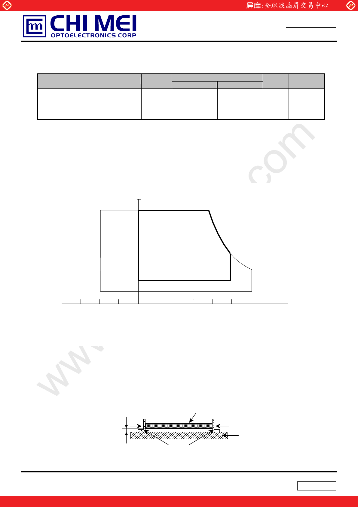
2.1 ABSOLUTE RATINGS OF ENVIRONMENT
Item Symbol
Storage Temperature TST -20 +60 ºC (1)
Operating Ambient Temperature TOP 0 +50 ºC (1), (2)
Shock (Non-Operating) S
Vibration (Non-Operating) V
Note (1) Temperature and relative humidity range is shown in the figure below.
(a) 90 %RH Max. (Ta Љ 40 ºC).
(b) Wet-bulb temperature should be 39 ºC Max. (Ta > 40 ºC).
(c) No condensation.
Note (2) The temperature of panel display surface area should be 0 ºC Min. and 60 ºC Max.
NOP
NOP
Min. Max.
ѧ
ѧ
Value
Unit Note
50 G (3), (5)
1.5 G (4), (5)
Relative Humidity (%RH)
100
90
80
60
Operating Range
40
20
10
Storage Range
Temperature (ºC)
Note (3) 11ms, half sine wave, 1 time for ± X, ± Y, ± Z.
8060-20 400 20-40
Note (4) 10 ~ 300 Hz, 10min/cycle, 3 cycles each X, Y, Z.
Note (5) At testing Vibration and Shock, the fixture in holding the module has to be hard and rigid enough
so that the module would not be twisted or bent by the fixture.
The fixing condition is shown as below:
t Room Temperature
Side Mount Fixing Screw
Gap=2mm
Bracket
LCD Module
Side Mount Fixing Screw
Stage
5 / 28
One step solution for LCD / PDP / OLED panel application: Datasheet, inventory and accessory!
Version 1.0
www.panelook.com
Page 6
Global LCD Panel Exchange Center
Issued Date: Aug. 30, 2006
www.panelook.com
Doc No.: 14068530
Model No.: M300F1-M01
Preliminary
2.2 ELECTRICAL ABSOLUTE RATINGS
2.2.1 TFT LCD MODULE
Item Symbol
Power Supply Voltage Vcc GND-0.3 21.0 V
Interface Type
Dual Link
TMDS
Min. Max.
2.2.2 BACKLIGHT UNIT
Item Symbol
Lamp Voltage VL --- 3.0K V
Lamp Current IL 3.0 6.5 mA
Lamp Frequency FL 40 80 KHz
Note (1) Permanent damage to the device may occur if maximum values are exceeded. Function operation
Min. Max.
Value
TMDS (Sil178 or Sil170 TX)
Value
Unit Note
(1)
Unit Note
(1), (2)
RMS
RMS
(1), (2)
should be restricted to the conditions described under Normal Operating Conditions.
Note (2) Specified values are for lamp (Refer to 3.2 for further information).
6 / 28
One step solution for LCD / PDP / OLED panel application: Datasheet, inventory and accessory!
Version 1.0
www.panelook.com
Page 7
Global LCD Panel Exchange Center
Issued Date: Aug. 30, 2006
www.panelook.com
Doc No.: 14068530
Model No.: M300F1-M01
Preliminary
3. ELECTRICAL CHARACTERISTICS
3.1 TFT LCD MODULE Ta = 25 ± 2 ºC
Parameter Symbol
Power Supply Voltage Vcc 17 18 19 V -
Ripple Voltage VRP 500 mV -
Rush Current I
White 900 1000 1100 mA (3)a
Power Supply Current
Vsync Frequency fV - 59.97 - Hz
Hsync Frequency fH - 74 - kHz
Main Frequency f
Note (1) The module should be always operated within above ranges.
Note (2) Measurement Conditions:
Black 540 640 740 mA (3)b
Vertical Stripe
RUSH
Icc
DCLK
Min. Typ. Max.
4.0 A (2)
1100 1200 1300 mA (3)c
- 134.25 - MHz
Value
Unit Note
Rush current I
can be measured when Vcc rising time is 470Ӵs.
RUSH
Vcc rising time is 470Ps
+5.0V
0.9Vcc
0.1Vcc
GND
470Ps
7 / 28
One step solution for LCD / PDP / OLED panel application: Datasheet, inventory and accessory!
Version 1.0
www.panelook.com
Page 8
Global LCD Panel Exchange Center
Issued Date: Aug. 30, 2006
www.panelook.com
Doc No.: 14068530
Model No.: M300F1-M01
Preliminary
Note (3) The specified power supply current is under the conditions at Vcc = 18.0 V, Ta = 25 ± 2 ºC, fV =
59.97 Hz, f
a. White Pattern
c. Vertical Stripe Pattern
= 134.25MHz whereas a power dissipation check pattern below is displayed.
DCLK
Active Area
b. Black Pattern
Active Area
R
G
R
B
G
R
B
G
B
B
B
R
R
R
G
G
G
B
B
B
R
R
Active Area
R R
G
B
G
B
8 / 28
One step solution for LCD / PDP / OLED panel application: Datasheet, inventory and accessory!
Version 1.0
www.panelook.com
Page 9
Global LCD Panel Exchange Center
www.panelook.com
Doc No.: 14068530
Issued Date: Aug. 30, 2006
Model No.: M300F1-M01
Preliminary
3.2 BACKLIGHT UNIT Ta = 25 ± 2 ºC
Parameter Symbol
Lamp Input Voltage V
Lamp Current I
Lamp Turn On Voltage V
Operating Frequency F
Lamp Life Time L
Power Consumption at
Gray level 255
Power Consumption at
Gray level 128
P
P
Power Consumption at
Gray level 0
P
L
BL
255
128
Min. Typ. Max.
L
1044 1160 1276
--- 5.5 ---
S
L
--- ---
--- ---
50 55 60
50000 --- ---
--- 102.08 ---
--- TBD ---
0
--- TBD ---
Value
mA
2250 (25 oC) V
2440 (0 oC) V
Unit Note
V
I
RMS
RMS
(2)
RMS
(2)
RMS
= 5.5 mA
L
(1)
KHz (3)
Hrs (5), IL= 5.5 mA
W (4), IL = 5.5 mA
W (4)
W (4)
Note (1) Lamp current is measured by current amplify & oscilloscope as shown below:
+
LCD
Module
ΗΗΗΗ
-
ΗΗΗΗ
Inverter
Current
Amplify
Oscilloscope
+
Current
Probe
Measure equipment:
Current Amplify: Tektronix TCPA300
Current probe: Tektronix TCP312
Oscilloscope: TDS3054B
Note (2) The voltage that must be larger than Vs should be applied to the lamp for more than 1 second
after startup. Otherwise, the lamp may not be turned on normally.
Note (3) The lamp frequency may produce interference with horizontal synchronization frequency from the
display, which might cause line flow on the display. In order to avoid interference, the lamp
frequency should be detached from the horizontal synchronization frequency and its harmonics as
far as possible.
Note (4) P
VL 16 x=255,128,0
= I
x
L
Note (5) The lifetime of lamp can be defined as the time in which it continues to operate under the condition
Ta = 25 2
o
C and IL = 5.5 mArms until one of the following events occurs:
(a) When the brightness becomes or lower than 50% of its original value.
(b) When the effective ignition length becomes or lower than 80% of its original value. (Effective
ignition length is defined as an area that has less than 70% brightness compared to the
brightness in the center point.)
9 / 28
One step solution for LCD / PDP / OLED panel application: Datasheet, inventory and accessory!
Version 1.0
www.panelook.com
Page 10

Global LCD Panel Exchange Center
Issued Date: Aug. 30, 2006
www.panelook.com
Doc No.: 14068530
Model No.: M300F1-M01
Preliminary
Note (6) The waveform of the voltage output of inverter must be area-symmetric and the design of the
inverter must have specifications for the modularized lamp. The performance of the Backlight,
such as lifetime or brightness, is greatly influenced by the characteristics of the DC-AC inverter for
the lamp. All the parameters of an inverter should be carefully designed to avoid producing too
much current leakage from high voltage output of the inverter. When designing or ordering the
inverter please make sure that a poor lighting caused by the mismatch of the Backlight and the
inverter (miss-lighting, flicker, etc.) never occurs. If the above situation is confirmed, the module
should be operated in the same manners when it is installed in your instrument.
The output of the inverter must have symmetrical (negative and positive) voltage waveform and
symmetrical current waveform.(Unsymmetrical ratio is less than 10%) Please do not use the inverter
which has unsymmetrical voltage and unsymmetrical current and spike wave. Lamp frequency may
produce interface with horizontal synchronous frequency and as a result this may cause beat on the
display. Therefore lamp frequency shall be as away possible from the horizontal synchronous
frequency and from its harmonics in order to prevent interference.
Requirements for a system inverter design, which is intended to have a better display performance, a
better power efficiency and a more reliable lamp. It shall help increase the lamp lifetime and reduce its
leakage current.
a. The asymmetry rate of the inverter waveform should be 10% below;
b. The distortion rate of the waveform should be within Ѕ2 ± 10%;
c. The ideal sine wave form shall be symmetric in positive and negative polarities
* Asymmetry rate:
I p
I -p
| I
* Distortion rate
I
– I –p | / I
p
(or I –p) / I
p
rms
rms
* 100%
10 / 28
One step solution for LCD / PDP / OLED panel application: Datasheet, inventory and accessory!
Version 1.0
www.panelook.com
Page 11

Global LCD Panel Exchange Center
Issued Date: Aug. 30, 2006
www.panelook.com
Doc No.: 14068530
Model No.: M300F1-M01
Preliminary
3.3 INVERTER SPECIFICATION
Symbol Description Condition Min. Typ. Max. Unit
Vin
lin
BLON Backlight ON/OFF Control
VDIM
lout(max) Vin=24V, VDIM=3.3V
lout(min)
Freq.
Vlamp
Vstart Lamp ignite voltage
Ts
Vpwm
Fpwm
Toff
Asymmetry Current waveform symmetrical
Distortion Current waveform distortion
Efficiency
Input Voltage
Input Current
Lamp Current Control
Output current
Lamp Frequency
Lamp voltage
Lamp ignite time
PWM signal
Shutdown time
ʳʳʳ
ʳ ʳ ˅˄ˁˉʳ ˅ˇʳ ˅ˉˁˇʳ
Vin=21.6V, VDIM=3.3V -- --ʳ
ON
OFF
ʳʳ ˃ʳ
Vin=24V, VDIM=0.0V 2.0 2.5 3.0 mArms
Vin=24V, VDIM=3.3V 50 55 60 KHz
ʳ 1053 1170 1287 Vrms
0к
25к
ʳ 1 -- 2 Sec.
High (ON)
Low (OFF) 0.0 --
ʳʳ
Lamp open 0.7 1 1.5 sec
ʳʳ
ʳʳ 0.9Ѕ2 Ѕ2ʳ 1.1Ѕ2
˅ˁˇʳ
˃ʳ
ˈˁ˃ʳ ˈˁˈʳ ˉˁ˃ʳ
-- -- 2440 Vrms
-- -- 2250 Vrms
˅ˁˈʳ
-- 160 240 Hz
-- -- 10 %
85 -- -- %
--
--
--
-- 5 V
ˈʳ
ˈˁˈʳ
˃ˁˋʳ
ˆˁˆʳ
˃ˁˋʳ
VDC
A
V
V
V
mArms
V
--
11 / 28
One step solution for LCD / PDP / OLED panel application: Datasheet, inventory and accessory!
Version 1.0
www.panelook.com
Page 12

Global LCD Panel Exchange Center
r
)
)
)
)
r
Issued Date: Aug. 30, 2006
www.panelook.com
Doc No.: 14068530
Model No.: M300F1-M01
Preliminary
4. BLOCK DIAGRAM
4.1 TFT LCD MODULE
(Starconn 093G30-B0001A)
INPUT CONNECTOR
RX2(+/-)
RX1(+/-)
RX0(+/-)
RXC(+/-)
RX5(+/-)
RX4(+/-)
RX3(+/-)
GND
DC Power
Supply
Power
connecto
VL
Inverter Connecto
4.2 BACKLIGHT UNIT
Dual TMDS INPUT /
TIMING CONTROLLER
DC/DC CONVERTER &
REFERENCE VOLTAGE
SCAN DRIVER IC
TFT LCD PANEL
(2560x1600)
DATA DRIVER IC
BACKLIGHT UNIT
HV (+
LV(-
HV (+
LV (-
12 / 28
One step solution for LCD / PDP / OLED panel application: Datasheet, inventory and accessory!
Version 1.0
www.panelook.com
Page 13

Global LCD Panel Exchange Center
Issued Date: Aug. 30, 2006
www.panelook.com
Doc No.: 14068530
Model No.: M300F1-M01
Preliminary
5. INPUT TERMINAL PIN ASSIGNMENT
5.1 INPUT SIGNAL
Pin Name Description
1 NC
NC NC
2
NC NC
3
4 NC
5 SHLD2 Shield for TMDS Channel 2
6 Rx2+ TMDS positive differential
7 Rx2- TMDS negative differential
8 SHLD1 Shield for TMDS Channel 1
9 Rx1+ TMDS positive differential
10 Rx1- TMDS negative differential
11 SHLD0 Shield for TMDS Channel 0
12 Rx0+ TMDS positive differential
13 Rx0- TMDS negative differential
14 SHLDC Shield for TMDS Channel C
15 Rxc+ TMDS positive differential
16 RxC- TMDS negative differential
17 SHLD5 Shield for TMDS Channel 5
18 Rx5+ TMDS positive differential
19 Rx5- TMDS negative differential
20 SHLD4 Shield for TMDS Channel 4
21 Rx4+ TMDS positive differential
22 Rx4- TMDS negative differential
23 SHLD3 Shield for TMDS Channel 3
24 Rx3+ TMDS positive differential
25 Rx3- TMDS negative differential
26 NC NC
27 NC NC
28 NC NC
29 NC NC
30 NC NC
Note (1) Connector Part No.: JAE FI-X30SSL-HF.or Compatible
NC
NC
13 / 28
One step solution for LCD / PDP / OLED panel application: Datasheet, inventory and accessory!
Version 1.0
www.panelook.com
Page 14

Global LCD Panel Exchange Center
Issued Date: Aug. 30, 2006
www.panelook.com
Doc No.: 14068530
Model No.: M300F1-M01
Preliminary
5.2 INPUT POWER
Pin Symbol Description Remark
1 GND Ground
2 GND Ground Reserved
3 PWR_ON LCM ON control signal input
4 GND Ground
5 V
6 V
7 V
8 V
9 GND Ground
10 NC NC
11 NC NC
12 GND Ground
13 HSYNC Hsync Output
14 VSYNC Vsync Output
15 PS_ON Dual/Single mode Output
Note (1) Connector (Receptacle): Molex 53261 or Compatible
LCD
LCD
LCD
LCD
LCM power supply, +18V
LCM power supply
LCM power supply
LCM power supply
(2) Matting connector (Plug): Molex 51021 or Compatible
5.3 INVERTER INPUT SIGNAL
Pin Symbol Description Remark
1 V
2
3
4
5
V
V
V
V
BL
BL
BL
BL
BL
Power Supply, +24V
Power Supply, +24V
Power Supply, +24V
Power Supply, +24V
Power Supply, +24V
6 GND Power Ground
7 GND Power Ground
8 GND Power Ground
9 GND Power Ground
10 GND Power Ground
11 NC No connection
˄˅ʳ
BLON Backlight On/Off Control signal
ONΚ2.4V~5.0V
OFFΚ0.0~0.8V
13 VDIM PWM Dimming control Signal Max 3.3V/Min 0.0V
˄ˇʳ
Status Lamp Operating Status
NormalΚ0~0.8V
AbnormalΚ3.0~5.0V
14 / 28
One step solution for LCD / PDP / OLED panel application: Datasheet, inventory and accessory!
Version 1.0
www.panelook.com
Page 15

Global LCD Panel Exchange Center
Issued Date: Aug. 30, 2006
www.panelook.com
Doc No.: 14068530
Model No.: M300F1-M01
Preliminary
5.4 COLOR DATA INPUT ASSIGNMENT
The brightness of each primary color (red, green and blue) is based on the 8-bit gray scale data input for
the color. The higher the binary input, the brighter the color. The table below provides the assignment of
color versus data input.
Data Signal
Basic
Colors
Gray
Scale
Of
Red
Color
Black
Red
Green
Blue
Cyan
Magenta
Yellow
White
Red(0) / Dark
Red(1)
Red(2)
Red(253)
Red(254)
Red(255)
R7 R6 R5 R4 R3 R2 R1 R0 R7 R6 G5 G4 G3 G2 G1 G0 R7 R6 B5 B4 B3 B2 B1 B0
0
0
1
1
0
0
0
0
0
0
1
1
1
1
1
1
0
0
0
0
0
0
:
:
:
:
:
:
1
1
1
1
1
1
Red Green Blue
0
0
0
0
0
0
0
0
0
0
0
0
0
0
0
0
0
0
0
0
0
1
1
1
1
1
1
0
0
0
0
0
0
0
0
0
0
0
0
0
0
0
0
0
0
0
0
0
1
1
1
1
1
1
1
1
0
0
0
0
0
0
0
0
0
0
0
0
0
0
0
0
0
0
0
0
0
1
1
1
1
1
1
1
0
0
0
0
0
0
1
1
1
1
1
1
1
1
1
1
1
1
1
1
1
1
1
1
1
1
1
0
0
0
0
0
0
0
0
1
1
1
1
1
1
1
1
1
1
1
1
1
1
1
1
1
1
1
1
1
0
0
0
0
0
0
0
1
1
1
1
1
1
1
1
1
1
1
1
1
1
1
1
1
1
1
1
1
0
0
0
0
0
0
0
0
0
0
0
0
0
0
0
0
0
0
0
0
0
0
0
0
0
0
1
0
0
0
0
0
0
0
0
0
0
0
0
0
0
0
0
0
0
0
1
0
0
0
0
0
0
0
0
0
0
0
0
0
0
0
0
:
:
:
:
:
:
:
:
:
:
:
:
:
:
:
:
:
:
:
:
:
:
:
:
:
:
:
:
:
:
:
:
:
:
:
:
:
:
:
:
:
:
1
1
1
1
0
1
0
0
0
0
0
0
0
0
0
0
0
0
0
0
0
1
1
1
1
1
0
0
0
0
0
0
0
0
0
0
0
0
0
0
0
0
1
1
1
1
1
1
0
0
0
0
0
0
0
0
0
0
0
0
0
0
0
0
0
0
1
1
1
0
1
0
0
0
:
:
0
0
0
Green(0) / Dark
Green(1)
Gray
Scale
Of
Green
Gray
Scale
Of
Blue
Note (1) 0: Low Level Voltage, 1: High Level Voltage
Green(2)
Green(253)
Green(254)
Green(255)
Blue(0) / Dark
Blue(1)
Blue(2)
Blue(253)
Blue(254)
Blue(255)
0
0
0
0
0
0
0
0
0
0
0
0
0
0
0
0
0
0
0
0
0
:
:
:
:
:
:
:
:
:
:
:
:
:
:
:
:
0
0
0
0
0
0
0
0
0
0
0
0
0
0
0
0
0
0
0
0
0
0
0
0
0
0
0
0
0
0
0
0
0
0
0
0
0
0
0
0
0
0
:
:
:
:
:
:
:
:
:
:
:
:
:
:
:
:
0
0
0
0
0
0
0
0
0
0
0
0
0
0
0
0
0
0
0
0
0
0
0
0
0
0
0
0
0
0
0
0
0
0
0
0
0
0
0
0
0
0
0
0
0
0
1
0
0
0
0
0
0
0
0
0
0
0
0
0
0
0
1
0
0
0
0
0
0
0
0
0
:
:
:
:
:
:
:
:
:
:
:
:
:
:
:
:
:
:
:
:
:
:
:
:
:
:
:
:
:
:
:
:
:
:
0
1
1
1
1
1
1
0
1
0
0
0
0
0
0
0
0
0
1
1
1
1
1
1
1
0
0
0
0
0
0
0
0
0
0
1
1
1
1
1
1
1
1
0
0
0
0
0
0
0
0
0
0
0
0
0
0
0
0
0
0
0
0
0
0
0
0
0
0
0
0
0
0
0
0
0
0
0
0
0
0
0
0
0
1
0
0
0
0
0
0
0
0
0
0
0
0
0
0
0
1
0
:
:
:
:
:
:
:
:
:
:
:
:
:
:
:
:
:
:
:
:
:
:
:
:
:
:
:
:
:
:
:
:
:
:
0
0
0
0
0
0
0
0
0
1
1
1
1
1
1
0
1
0
0
0
0
0
0
0
0
0
1
1
1
1
1
1
1
0
0
0
0
0
0
0
0
0
0
1
1
1
1
1
1
1
1
15 / 28
One step solution for LCD / PDP / OLED panel application: Datasheet, inventory and accessory!
Version 1.0
www.panelook.com
Page 16

Global LCD Panel Exchange Center
www.panelook.com
Doc No.: 14068530
Issued Date: Aug. 30, 2006
Model No.: M300F1-M01
Preliminary
6. INTERFACE TIMING
6.1 INPUT SIGNAL TIMING SPECIFICATIONS (Dual ModeΚ2560 1600)
The input signal timing specifications are shown as the following table and timing diagram.
Signal Item Symbol Min. Typ. Max. Unit Note
DCLK
HSync
VSync
Data Enable
Period t
Frequency f
Width-Total t
Period t
Frequency f
Width t
Width-Total t
Period t
Frequency f
Width t
Horizontal Valid t
Horizontal Back Porch t
Horizontal Front Porch t
Horizontal Blank Vertical Valid t
Vertical Back Porch t
Vertical Front Porch t
CLK
CLK
HP
HP
H
WH
VT
VP
V
WV
HV
HBP
HFP
VV
VBP
VFP
Vertical Blank -
Note: This module is operated by DE only mode.
7.45 7.45 7.45 ns
134.25 134.25 134.25 MHz 268.5/2
2720 2720 2720 Tc
10.13 10.13 10.13 us
98.71 98.71 98.71 kHz
32 32 32 t
1646 1646 1646 t
CLK
HP
16.68 16.68 16.68
59.97 59.97 59.97 Hz
6 6 6 t
HP
2560 2560 2560
80 80 80
48 48 48
t
CLK
160 160 160
1600 1600 1600
38 38 38
2 2 2
t
HP
46 46 46
tWH+ t
tWV + t
HBP
VBP
-
-
-
-
-
-
-
-
-
-
+ t
HFP
-
-
+ t
VFP
16 / 28
One step solution for LCD / PDP / OLED panel application: Datasheet, inventory and accessory!
Version 1.0
www.panelook.com
Page 17

Global LCD Panel Exchange Center
Issued Date: Aug. 30, 2006
www.panelook.com
Doc No.: 14068530
Model No.: M300F1-M01
Preliminary
6.2 SIGNAL TIMING WAVEFORMS
17 / 28
One step solution for LCD / PDP / OLED panel application: Datasheet, inventory and accessory!
Version 1.0
www.panelook.com
Page 18

Global LCD Panel Exchange Center
www.panelook.com
Doc No.: 14068530
Issued Date: Aug. 30, 2006
Model No.: M300F1-M01
Preliminary
6.3 POWER ON/OFF SEQUENCE
To prevent a latch-up or DC operation of LCD module, the power on/off sequence should be as the
diagram below.
Power Supply
for LCD, Vcc
0V
- Interface Signal
(LVDS Signal of
Transmitter), V
0V
I
- Power for Lamp
Timing Specifications:
0.5< t1 Љ 10 msec
0 < t2 Љ 50 msec
0 < t3 Љ 50 msec
t4 Њ 500 msec
Power On
90%
10%
Power Off
90%
t1
t3t2
Valid Data
t6t5
50%50%
ONOFF OFF
Restart
10%
t4
t5 Њ 500 msec
t6 Њ 90 msec
18 / 28
One step solution for LCD / PDP / OLED panel application: Datasheet, inventory and accessory!
Version 1.0
www.panelook.com
Page 19

Global LCD Panel Exchange Center
Issued Date: Aug. 30, 2006
www.panelook.com
Doc No.: 14068530
Model No.: M300F1-M01
Preliminary
7. OPTICAL CHARACTERISTICS
7.1 TEST CONDITIONS
Item Symbol Value Unit
Ambient Temperature Ta
Ambient Humidity Ha
Supply Voltage VCC 5.0 V
Input Signal According to typical value in "3. ELECTRICAL CHARACTERISTICS"
Lamp Current IL 5.5 mA
Inverter Operating Frequency FL 55 KHz
Inverter VK.89144.109
25r2
50r10
7.2 OPTICAL SPECIFICATIONS
The relative measurement methods of optical characteristics are shown in 7.2. The following items should
be measured under the test conditions described in 7.1 and stable environment shown in Note (5).
o
C
%RH
Item Symbol Condition Min. Typ. Max. Unit Note
Red
Color
Chromaticity
(CIE 1931)
Center Luminance of White
(Center of Screen)
Contrast Ratio CR
Gray to Gray Response Time T
White Variation
Viewing Angle
Green
Blue
White
Horizontal
Vertica l
Rx
Ry
Gx
Gy
Bx (0.154)
By
Wx 0.313
Wy
L
C
GtG_AVE_
GW
Tx+
-
T
x
TY+
T
-
Y
T
=0q, TY =0q
x
CS-1000T
Tx=0q, TY =0q
T
=0q, TY =0q
x
USB2000
CR Њ 10
USB2000
TYP
-0.03
220 300 cd/m2(3), (5)
700 1000 --- --- (2), (5)
(0.648)
(0.335)
(0.285)
(0.608)
TYP
+0.03
--- (1), (5)
(0.087)
0.329
---
--- 1.25 1.4 - (5), (6)
80 88 --80 88 --80 88 --80 88 ---
8 12 ms (4)
Deg. (1), (5)
19 / 28
One step solution for LCD / PDP / OLED panel application: Datasheet, inventory and accessory!
Version 1.0
www.panelook.com
Page 20

Global LCD Panel Exchange Center
y
y
y
www.panelook.com
Doc No.: 14068530
Issued Date: Aug. 30, 2006
Model No.: M300F1-M01
Preliminary
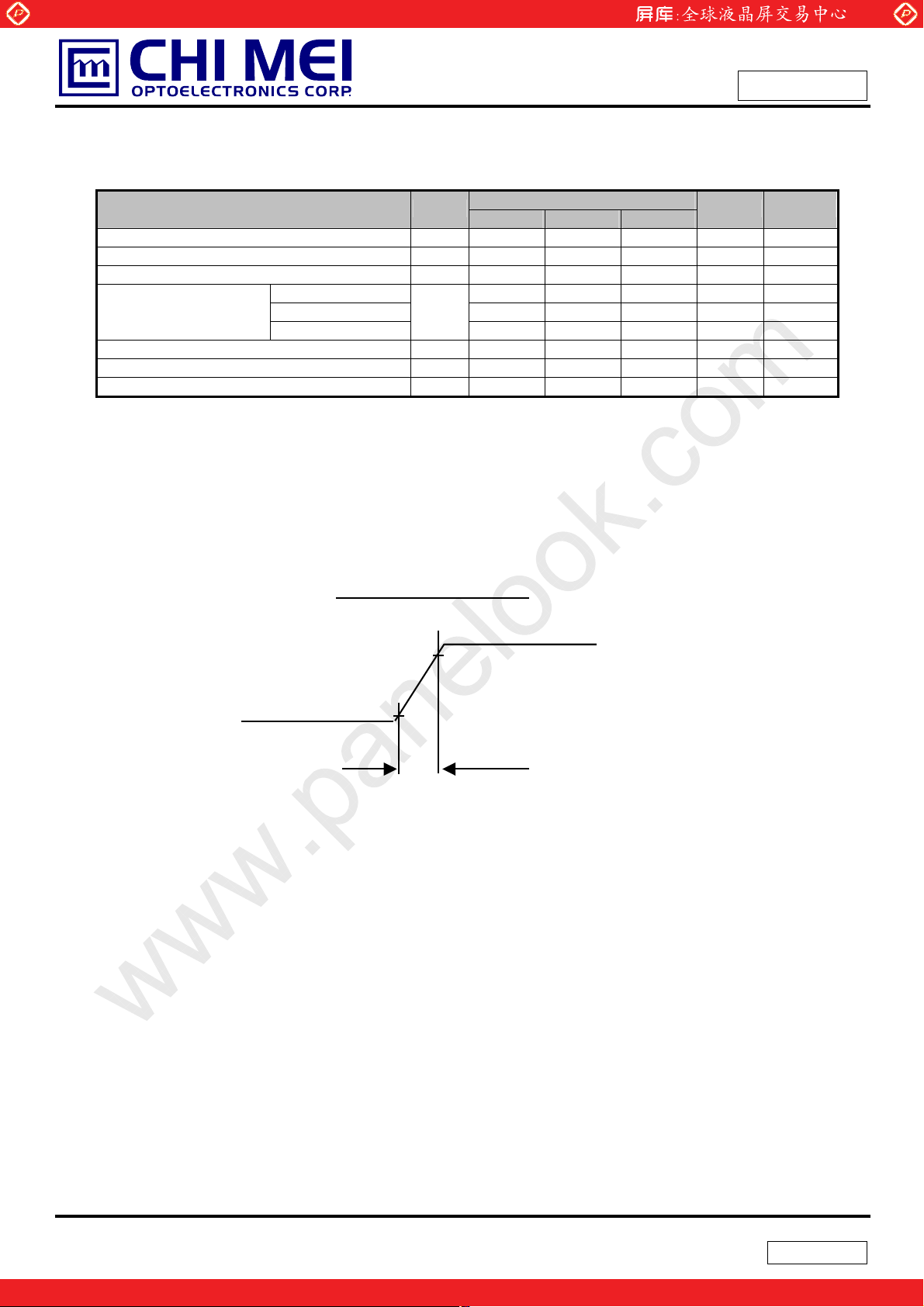
Note (1) Definition of Viewing Angle (Tx, Ty):
Normal
TX- = 90º
6 o’clock
T
- = 90º
x-
y-
Note (2) Definition of Contrast Ratio (CR):
The contrast ratio can be calculated by the following expression.
Contrast Ratio (CR) = L255 / L0
L255: Luminance of gray level 255
L 0: Luminance of gray level 0
Tx = T
= 0º
Ty- Ty
Tx
Tx
12 o’clock direction
y+
T
+ = 90º
x+
TX+ = 90º
CR = CR (1)
CR (X) is corresponding to the Contrast Ratio of the point X at Figure in Note (6).
Note (3) Definition of Luminance of White (L
Measure the luminance of gray level 255 at center point
L
= L (1)
C
L (x) is corresponding to the luminance of the point X at Figure in Note (6).
Note (4) Definition of Response Time (T
T
GTG_AVE
is defined as the total average response time for “Gray To Gray “.
The Gray to Gray response time is defined as the following chart.
Gray to Gray
G0
G63
Initial Gray
G127
G191
G255
):
C
):
GTG_AVE
Target Gray
G0 G63 G127 G191 G255
20 / 28
One step solution for LCD / PDP / OLED panel application: Datasheet, inventory and accessory!
Version 1.0
www.panelook.com
Page 21

Global LCD Panel Exchange Center
Issued Date: Aug. 30, 2006
www.panelook.com
Doc No.: 14068530
Model No.: M300F1-M01
Preliminary
Note (5) Measurement Setup:
The LCD module should be stabilized at given temperature for 30 minutes to avoid abrupt
temperature change during measuring. In order to stabilize the luminance, the measurement
should be executed after lighting Backlight for 30 minutes in a windless room.
LCD Module
LCD Panel
USB2000
Center of the Screen
CS-1000T
Field of View = 2º
Note (6) Definition of White Variation (GW):
Measure the luminance of gray level 255 at 13 points
Maximum [L(1), L(2), L(3), L(4), L(5), L(6), L(7), L(8), L(9), L(10), L(11), L(12), L(13)]
GW =
Minimum [L(1), L(2), L(3), L(4), L(5), L(6), L(7), L(8), L(9), L(10), L(11), L(12), L(13)]
Light Shield Room
(Ambient Luminance < 2 lux)
21 / 28
One step solution for LCD / PDP / OLED panel application: Datasheet, inventory and accessory!
Version 1.0
www.panelook.com
Page 22

Global LCD Panel Exchange Center
X
A
Issued Date: Aug. 30, 2006
www.panelook.com
Doc No.: 14068530
Model No.: M300F1-M01
Preliminary
˄˂˄˃˛
ˉ
˛˂ˇ
˛˂ˇ˛˂ˇ
˛
ˌ
Vertical Line Number
˛˂ˇ
˄˄
˄˂˄˃˛
Horizontal Line Number
˅
ˇ
˄˂˄˃˪
˪˂ˇ ˪˂ˇ
ˊ
˄
˄˅
˪
ctive Area
˪˂ˇ
ˋ
ˆ
˄˃
ΚTest Point
XЈ1 to 13
ˈ
˄ˆ
˄˂˄˃˪
˪˂ˇ
8. PACKAGING
8.1 PACKING SPECIFICATIONS
(1) 5 LCD modules / 1 Box
(2) Box dimensions: 680(L) X 400(W) X 360(H) mm
(3) Weight: approximately 17.5Kg (5 modules per box)
8.2 PACKING METHOD
(1) Carton Packing should have no failure in the following reliability test items.
Test Item Test Conditions Note
ISTA STANDARD
Random, Frequency Range: 1 – 200 Hz
Vibration
Dropping Test 1 Angle, 3 Edge, 6 Face, 60cm Non Operation
Top & Bottom: 30 minutes (+Z), 10 min (-Z),
Right & Left: 10 minutes (X)
Back & Forth 10 minutes (Y)
Non Operation
22 / 28
One step solution for LCD / PDP / OLED panel application: Datasheet, inventory and accessory!
Version 1.0
www.panelook.com
Page 23

Global LCD Panel Exchange Center
Issued Date: Aug. 30, 2006
www.panelook.com
Doc No.: 14068530
Model No.: M300F1-M01
Preliminary
For ocean shipping
Figure. 8-1 Packing method
23 / 28
One step solution for LCD / PDP / OLED panel application: Datasheet, inventory and accessory!
Version 1.0
www.panelook.com
Page 24

Global LCD Panel Exchange Center
Issued Date: Aug. 30, 2006
www.panelook.com
Doc No.: 14068530
Model No.: M300F1-M01
Preliminary
For air transport
Figure. 8-2 Packing method
Figure. 8-3 Packing method
Figure. 8-3 Packing method
9. DEFINITION OF LABELS
9.1 CMO MODULE LABEL
The barcode nameplate is pasted on each module as illustration, and its definitions are as following explanation.
24 / 28
One step solution for LCD / PDP / OLED panel application: Datasheet, inventory and accessory!
Version 1.0
www.panelook.com
Page 25

Global LCD Panel Exchange Center
www.panelook.com
Doc No.: 14068530
Issued Date: Aug. 30, 2006
Model No.: M300F1-M01
Preliminary
(a) Model Name: M300F1-M01
(b) Revision: Rev. XX, for example: A0, A1… B1, B2… or C1, C2…etc.
(c) CMO barcode definition:
Serial ID: XX
-XX-X-XX-YMD-L-NNNN
Code Meaning Description
XX CMO internal use -
XX Revision Cover all the change
X CMO internal use -
XX CMO internal use -
Year: 2001=1, 2002=2, 2003=3, 2004=4…
YMD Year, month, day
Month: 1~12=1, 2, 3, ~, 9, A, B, C
Day: 1~31=1, 2, 3, ~, 9, A, B, C, ~, W, X, Y, exclude I, O, and U.
L Product line # Line 1=1, Line 2=2, Line 3=3, …
NNNN Serial number Manufacturing sequence of product
(d) Customer’s barcode definition:
Serial ID: CM
-30F11-X-X-X-XX-L-XX-L-YMD-NNNN
Code Meaning Description
CM Supplier code CMO=CM
30F11 Model number M300F1-M01 = 30F11
X Revision code Non ZBD: 1,~,9,0 / ZBD: A~Z
X Source driver IC code
X Gate driver IC code
Century=1, CLL=2, Demos=3, Epson=4, Fujitsu=5, Himax=6, Hitachi=7, Hynix=8,
LDI=9, Matsushita=A, NEC=B, Novatec=C, OKI=D, Philips=E, Renasas=F,
Samsung=G, Sanyo=H, Sharp=I, TI=J, Topro=K, Toshiba=L, Windbond=M
XX Cell location Tainan Taiwan=TN, Ningbo China=CN
L Cell line # 1~12=0~C
XX Module location Tainan Taiwan=TN, Ningbo China=CN
L Module line # 1~12=0~C
Year: 2001=1, 2002=2, 2003=3, 2004=4…
YMD Year, month, day
Month: 1~12=1, 2, 3, ~, 9, A, B, C
Day: 1~31=1, 2, 3, ~, 9, A, B, C, ~, T, U, V
NNNN Serial number By LCD supplier
10. PRECAUTIONS
10.1 ASSEMBLY AND HANDLING PRECAUTIONS
(1) Do not apply rough force such as bending or twisting to the module during assembly.
25 / 28
One step solution for LCD / PDP / OLED panel application: Datasheet, inventory and accessory!
Version 1.0
www.panelook.com
Page 26

Global LCD Panel Exchange Center
Issued Date: Aug. 30, 2006
www.panelook.com
Doc No.: 14068530
Model No.: M300F1-M01
Preliminary
(2) To assemble or install module into user’s system can be only in clean working areas. The dust and oil
may cause electrical short or worsen the polarizer.
(3) It’s not permitted to have pressure or impulse on the module because the LCD panel and Backlight will
be damaged.
(4) Always follow the correct power sequence when LCD module is connecting and operating. This can
prevent damage to the CMOS LSI chips during latch-up.
(5) Do not pull the I/F connector in or out while the module is operating.
(6) Do not disassemble the module.
(7) Use a soft dry cloth without chemicals for cleaning, because the surface of polarizer is very soft and
easily scratched.
(8) It is dangerous that moisture come into or contacted the LCD module, because moisture may damage
LCD module when it is operating.
(9) High temperature or humidity may reduce the performance of module. Please store LCD module within
the specified storage conditions.
(10) When ambient temperature is lower than 10ºC may reduce the display quality. For example, the
response time will become slowly, and the starting voltage of CCFL will be higher than room
temperature.
10.2 SAFETY PRECAUTIONS
(1) The startup voltage of Backlight is approximately 1000 Volts. It may cause electrical shock while
assembling with inverter. Do not disassemble the module or insert anything into the Backlight unit.
(2) If the liquid crystal material leaks from the panel, it should be kept away from the eyes or mouth. In
case of contact with hands, skin or clothes, it has to be washed away thoroughly with soap.
(3) After the module’s end of life, it is not harmful in case of normal operation and storage.
26 / 28
One step solution for LCD / PDP / OLED panel application: Datasheet, inventory and accessory!
Version 1.0
www.panelook.com
Page 27

www.panelook.com
www.panelook.com
Global LCD Panel Exchange Center
One step solution for LCD / PDP / OLED panel application: Datasheet, inventory and accessory!
Page 28

 Loading...