

CMO M260J5-L01 Specification
Global LCD Panel Exchange Center
ுழၴ ຝ ᐉு ߡۥ ދป
ขጥ
吳
柏 勳
Issued Date: Apr.27, 2009
www.panelook.com
Model No.: M260J5-L01
Tentative
TFT LCD Approval Specification
MODEL NO.: M260J5- L01
Customer:
Approved by:
Note:
MTR
2009-07-03
17:41:54
One step solution for LCD / PDP / OLED panel application: Datasheet, inventory and accessory!
2009.07.03
1 / 26
Director Accept
Version 0.0
www.panelook.com
Global LCD Panel Exchange Center
Issued Date: Apr.27, 2009
www.panelook.com
Model No.: M260J5-L01
Tentative
- CONTENTS -
REVISION HISTORY ............................................................................................................................... 3
1. GENERAL DESCRIPTION .................................................................................................................. 4
1.1 OVERVIEW
1.2 FEATURES
1.3 APPLICATION
1.4 GENERAL SPECIFICATIONS
1.5 MECHANICAL SPECIFICATIONS
2. ABSOLUTE MAXIMUM RATINGS ....................................................................................................... 5
2.1 ABSOLUTE RATINGS OF ENVIRONMENT
2.2 ELECTRICAL ABSOLUTE RATINGS
2.2.1 TFT LCD MODULE
2.2.2 BACKLIGHT UNIT
3. ELECTRICAL CHARACTERISTICS .................................................................................................... 7
3.1 TFT LCD MODULE
3.2 BACKLIGHT UNIT
4. BLOCK DIAGRAM ............................................................................................................................... 11
4.1 TFT LCD MODULE
4.2 BACKLIGHT UNIT
5. INPUT TERMINAL PIN ASSIGNMENT................................................................................................ 12
5.1 TFT LCD MODULE
5.2 LVDS DATA MAPPING TABLE
5.3 BACKLIGHT UNIT
5.4 COLOR DATA INPUT ASSIGNMENT
6. INTERFACE TIMING ...........................................................................................................................15
6.1 INPUT SIGNAL TIMING SPECIFICATIONS
6.2 POWER ON/OFF SEQUENCE
7. OPTICAL CHARACTERISTICS........................................................................................................... 17
7.1 TEST CONDITIONS
7.2 OPTICAL SPECIFICATIONS
8. PACKAGING ........................................................................................................................................ 22
8.1 PACKING SPECIFICATIONS
8.2 PACKING METHOD
9. DEFINITION OF LABELS .................................................................................................................... 24
10. PRECAUTIONS ................................................................................................................................. 25
10.1 ASSEMBLY AND HANDLING PRECAUTIONS
10.2 SAFETY PRECAUTIONS
11. MECHANICAL CHARACTERISTICS................................................................................................. 26
2 / 26
One step solution for LCD / PDP / OLED panel application: Datasheet, inventory and accessory!
Version 0.0
www.panelook.com
Global LCD Panel Exchange Center
Issued Date: Apr.27, 2009
www.panelook.com
Model No.: M260J5-L01
Tentative
REVISION HISTORY
Version Date Section Description
Ver 0.0 Apr.27 , 09’ - M260J5 -L01 Tentative specifications was first issued.
3 / 26
One step solution for LCD / PDP / OLED panel application: Datasheet, inventory and accessory!
Version 0.0
www.panelook.com
Global LCD Panel Exchange Center
Issued Date: Apr.27, 2009
www.panelook.com
Model No.: M260J5-L01
Tentative
1. GENERAL DESCRIPTION
1.1 OVERVIEW
M260J5-L01 is a 25.54” TFT Liquid Crystal Display module with 4 CCFL Backlight unit and 30 pins
2ch-LVDS interface. This module supports 1920 x 1200 WUXGA mode and can display up to 16.7M colors.
The inverter module for Backlight is not built in.
1.2 FEATURES
- Extra-wide viewing angle.
- High contrast ratio.
- Fast response time.
- WUXGA (1920 x 1200 pixels) resolution.
- DE (Data Enable) only mode.
- LVDS (Low Voltage Differential Signaling) interface.
- RoHS compliance.
1.3 APPLICATION
- TFT LCD Monitor
1.4 GENERAL SPECIFICATI0NS
Item Specification Unit Note
Active Area 550.08 (H) x 343.8 (V) (25.54” diagonal) mm
Bezel Opening Area 554.1 (H) x 347.8 (V) mm
Driver Element a-Si TFT active matrix - -
Pixel Number 1920 x R.G.B. x 1200 pixel -
Pixel Pitch 0.2865 (H) x 0.2865 (V) mm -
Pixel Arrangement RGB vertical stripe - -
Display Colors 16.7M color -
Transmissive Mode Normally White - -
Surface Treatment AG type, 3H hard coating, Haze 25
Module Power Consumption 33.05 Watt (2)
(1)
1.5 MECHANICAL SPECIFICATIONS
Item Min. Typ. Max. Unit Note
Horizontal(H) 577.8 578.3 578.8 mm
Module Size
Note (1) Please refer to the attached drawings for more information of front and back outline dimensions.
Note (2) Please refer to sec.3.1 & 3.2 for more information of power consumption.
Vertical(V) 368.35 368.85 369.35 mm
Depth(D) 15.8 16.3 16.8 mm
Weight - 3310 3360 g -
4 / 26
One step solution for LCD / PDP / OLED panel application: Datasheet, inventory and accessory!
(1)
Version 0.0
www.panelook.com
Global LCD Panel Exchange Center
A
Issued Date: Apr.27, 2009
www.panelook.com
Model No.: M260J5-L01
Tentative
2. ABSOLUTE MAXIMUM RATINGS
2.1 ABSOLUTE RATINGS OF ENVIRONMENT
Item Symbol
Storage Temperature TST -20 60 ºC (1)
Operating Ambient Temperature TOP 0 50 ºC (1), (2)
Shock (Non-Operating) S
Vibration (Non-Operating) V
LCD Cell Life Time L
Note (1) Temperature and relative humidity range is shown in the figure below.
(a) 90 %RH Max. (Ta Љ 40 ºC).
(b) Wet-bulb temperature should be 39 ºC Max. (Ta > 40 ºC).
(c) No condensation.
- 50 G (3), (5)
NOP
1.5 G (4), (5)
NOP
50,000 - Hrs
CELL
Min. Max.
Value
Unit Note
MTBF
based
Note (2) The temperature of panel display surface area should be 0 ºC Min. and 60 ºC Max.
Relative Humidity (%RH)
100
90
80
60
Operating Range
40
20
10
Storage Range
Temperature (ºC)
8060-20 40 0 20 -40
Note (3) 11ms, half sine wave, 1 time for ± X, ± Y, ± Z.
Note (4) 10 ~ 300 Hz, 10min/cycle, 3 cycles each X, Y, Z.
Note (5) At testing Vibration and Shock, the fixture in holding the module has to be hard and rigid enough
so that the module would not be twisted or bent by the fixture.
The fixing condition is shown as below:
t Room Temperature
Side Mount Fixing Screw
Gap=2mm
Bracket
LCD Module
Side Mount Fixing Screw
Stage
5 / 26
One step solution for LCD / PDP / OLED panel application: Datasheet, inventory and accessory!
Version 0.0
www.panelook.com
Global LCD Panel Exchange Center
Issued Date: Apr.27, 2009
www.panelook.com
Model No.: M260J5-L01
Tentative
2.2 ELECTRICAL ABSOLUTE RATINGS
2.2.1 TFT LCD MODULE
Item Symbol
Power Supply Voltage Vcc -0.3 +6.0 V (1)
Logic Input Voltage Vlogic -0.3 +3.6 V
Min. Max.
2.2.2 BACKLIGHT UNIT
Item Symbol
Lamp Voltage VL -- 2.5K V
Lamp Current IL 3.0 8.0 mA
Lamp Frequency FL 40 80 KHz
Note (1) Permanent damage to the device may occur if maximum values are exceeded. Function operation
should be restricted to the conditions described under Normal Operating Conditions.
Min. Max.
Value
Value
Unit Note
Unit Note
(1), (2)
RMS
RMS
(1), (2)
Note (2) Specified values are for lamp (Refer to 3.2 for further information).
6 / 26
One step solution for LCD / PDP / OLED panel application: Datasheet, inventory and accessory!
Version 0.0
www.panelook.com
Global LCD Panel Exchange Center
Issued Date: Apr.27, 2009
www.panelook.com
Model No.: M260J5-L01
Tentative
3. ELECTRICAL CHARACTERISTICS
3.1 TFT LCD MODULE Ta = 25 ± 2 ºC
Parameter Symbol
Min. Typ. Max.
Power Supply Voltage Vcc 4.5 5.0 5.5 V -
Ripple Voltage VRP - - 100 mV -
Rush Current I
Power Supply Current
Power Consumption P
RUSH
White (0.65) (0.81) A (3)a
Black (1.23) (1.45) A (3)b
Vertical Stripe
-
-
-
LCD
(3) A (2)
(1.21) (1.34) A (3)c
(6.15) (7.25) Watt (4)
LVDS differential input voltage Vid 100 - 600 mV
LVDS common input voltage Vic - 1.2 - V
Logic High Input Voltage VIH 2.64 3.6 V
Logic Low Input Voltage VIL -0.3 0.66 V
Note (1) The module should be always operated within above ranges.
Value
Unit Note
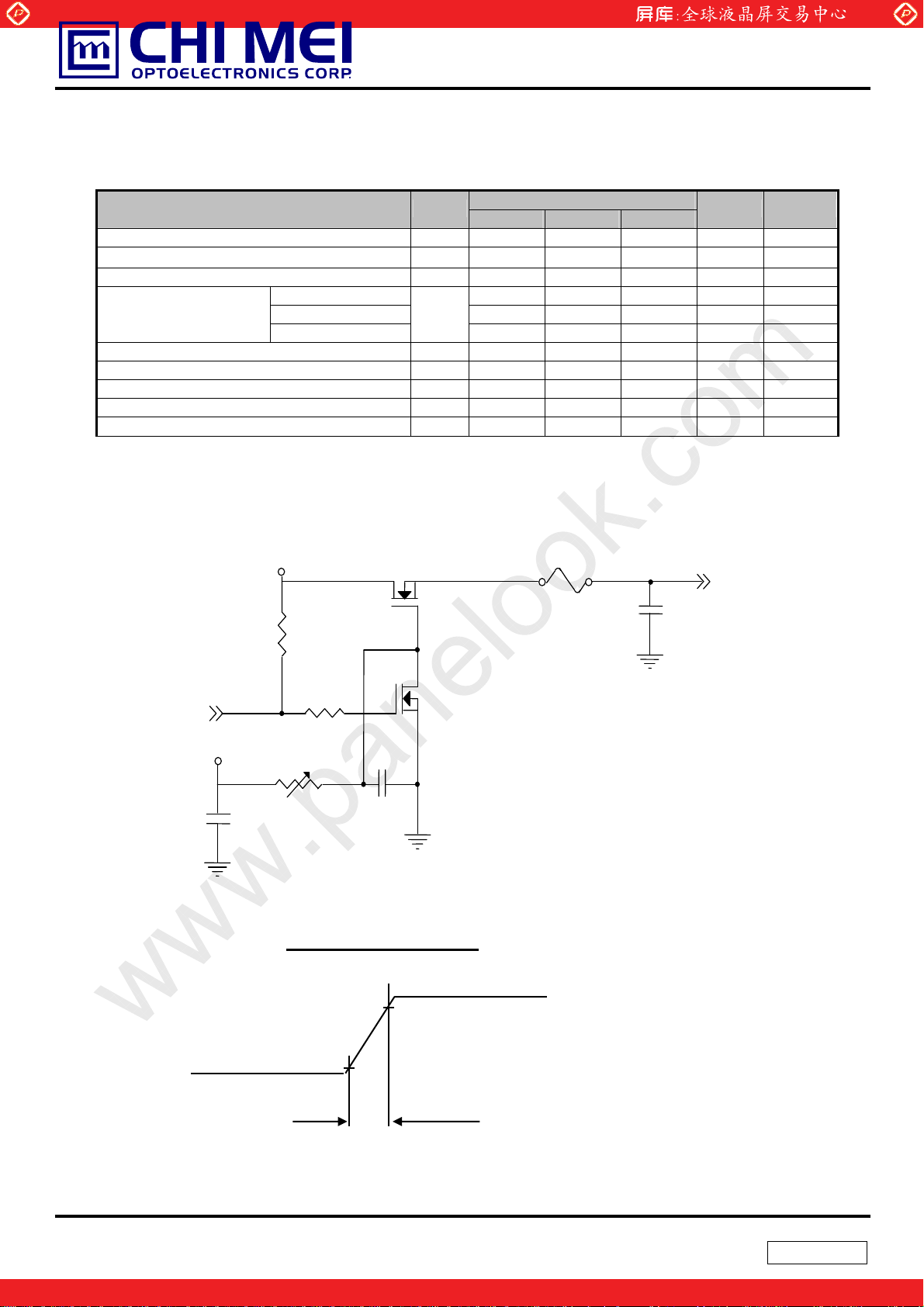
Note (2) Measurement Conditions:
+5.0V
R1
47K
(High to Low)
(Control Signal)
SW
+12V
C1
1uF
VR1
R2
1K
47K
Q1 2SK147 5
C2
0.01uF
Q2
2SK1470
FUSE
C3
1uF
Vcc
(LCD Module Input)
Vcc rising time is 470μs
Vcc
0.9Vcc
0.1Vcc
GND
470μs
7 / 26
One step solution for LCD / PDP / OLED panel application: Datasheet, inventory and accessory!
Version 0.0
www.panelook.com
Global LCD Panel Exchange Center
≤≤≤
Issued Date: Apr.27, 2009
www.panelook.com
Model No.: M260J5-L01
Tentative
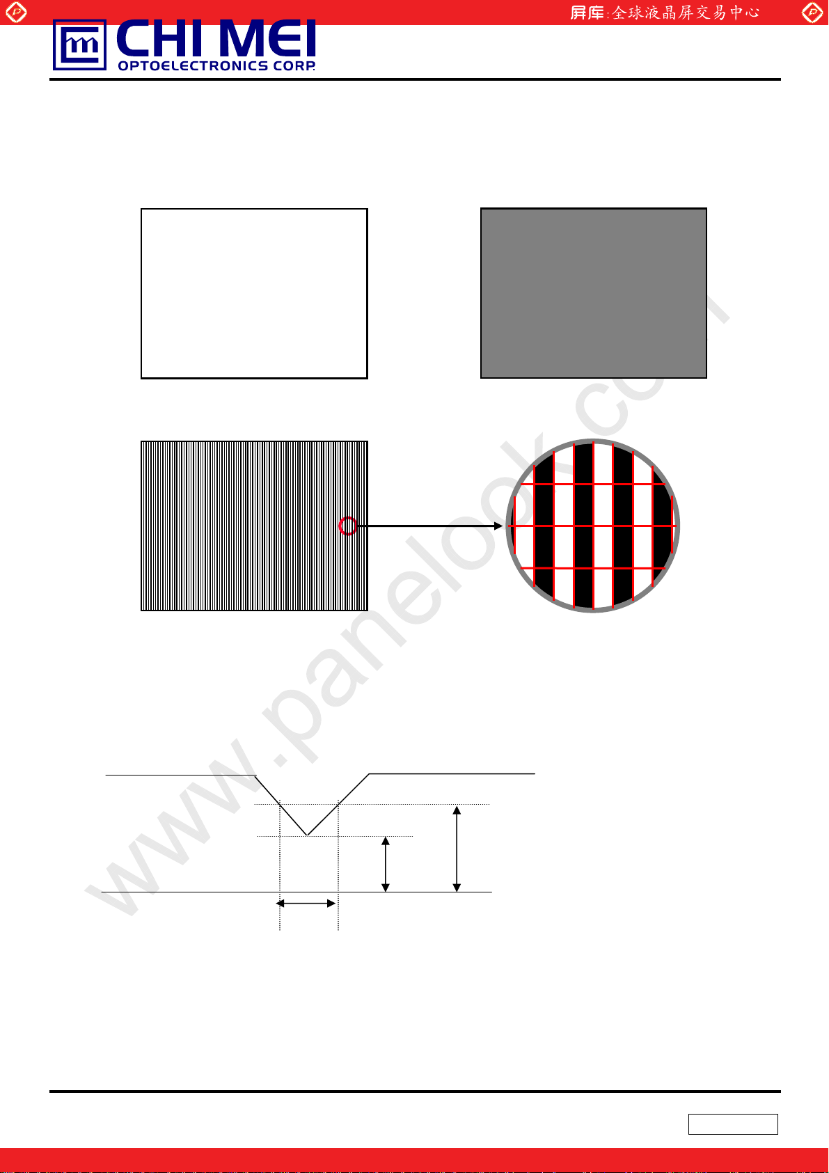
Note (3) The specified power supply current is under the conditions at Vcc = 5.0 V, Ta = 25 ± 2 ºC, fv = 60
Hz, whereas a power dissipation check pattern below is displayed.
a. White Pattern
Active Area
c. Vertical Stripe Pattern
b. Black Pattern
Active Area
R
G
R
B
G
R
B
G
R R
G
B
B
B
B
R
R
R
G
G
G
G
B
B
B
B
R
R
Active Area
Note (4) The power consumption is specified at the pattern with the maximum current.
3.1.2 Vcc Power Dip Condition:
Vcc
4.5V
4.0V
Td
Dip condition:
msTdVVccV 20,5.40.4
8 / 26
One step solution for LCD / PDP / OLED panel application: Datasheet, inventory and accessory!
Version 0.0
www.panelook.com
 Loading...