

Page 1
Global LCD Panel Exchange Center
ಖᙕ
ՠ܂
ᐉு
ߡۥ
ދป
Issued Date: Feb. 26, 2007
www.panelook.com
Doc No.:
Model No.: M240J1-L03
Approval
TFT LCD Approval Specification
MODEL NO.: M240J1- L03
Customer: JVC
Approved by:
Note:
2007-03-05
21:22:50 CST
2007-02-26
15:18:15 CST
One step solution for LCD / PDP / OLED panel application: Datasheet, inventory and accessory!
Approve by
Dept. Mgr.(QA
RA)
Approve by
Director
tomy_chen(ຫةԫ
/52720/54140/43150)
teren_lin(ࣥո
/56910/36064)
1 / 30
Department
Manager(QA RA)
Director Accept
Accept
Version 3.0
www.panelook.com
Page 2
Global LCD Panel Exchange Center
Issued Date: Feb. 26, 2007
www.panelook.com
Doc No.:
Model No.: M240J1-L03
Approval
- CONTENTS -
REVISION HISTORY ............................................................................................................................... 3
1. GENERAL DESCRIPTION .................................................................................................................. 4
1.1 OVERVIEW
1.2 FEATURES
1.3 APPLICATION
1.4 GENERAL SPECIFICATIONS
1.5 MECHANICAL SPECIFICATIONS
2. ABSOLUTE MAXIMUM RATINGS ....................................................................................................... 5
2.1 ABSOLUTE RATINGS OF ENVIRONMENT
2.2 ELECTRICAL ABSOLUTE RATINGS
2.2.1 TFT LCD MODULE
2.2.2 BACKLIGHT UNIT
3. ELECTRICAL CHARACTERISTICS .................................................................................................... 7
3.1 TFT LCD MODULE
3.2 BACKLIGHT UNIT
4. BLOCK DIAGRAM ............................................................................................................................... 9
4.1 TFT LCD MODULE
4.2 BACKLIGHT UNIT
5. INPUT TERMINAL PIN ASSIGNMENT................................................................................................ 10
5.1 TFT LCD MODULE
5.2 BACKLIGHT UNIT
5.3 COLOR DATA INPUT ASSIGNMENT
6. INVERTER SPECIFICATIONS ............................................................................................................ 13
6.1 CONNECTOR TYPE
6.2 INPUT CONNECTOR PIN ASSIGNMENT
6.3 OUTPUT CONNECTOR PIN ASSIGNMENT
6.4 GENERAL ELECTRICAL SPECIFICATION
7. INTERFACE TIMING ...........................................................................................................................18
7.1 INPUT SIGNAL TIMING SPECIFICATIONS
7.2 POWER ON/OFF SEQUENCE
8. OPTICAL CHARACTERISTICS........................................................................................................... 20
8.1 TEST CONDITIONS
8.2 OPTICAL SPECIFICATIONS
9. PACKAGING ........................................................................................................................................ 25
9.1 PACKING SPECIFICATIONS
9.2 PACKING METHOD
10. DEFINITION OF LABELS .................................................................................................................. 27
11. PRECAUTIONS ................................................................................................................................. 28
11.1 ASSEMBLY AND HANDLING PRECAUTIONS
11.2 SAFETY PRECAUTIONS
11. MECHANICAL CHARACTERISTICS ................................................................................................. 29
2 / 30
One step solution for LCD / PDP / OLED panel application: Datasheet, inventory and accessory!
Version 3.0
www.panelook.com
Page 3

Global LCD Panel Exchange Center
Issued Date: Feb. 26, 2007
www.panelook.com
Doc No.:
Model No.: M240J1-L03
Approval
REVISION HISTORY
Version Date Section Description
Ver 2.0
Ver 3.0
Oct. 9, 06’
Feb. 26, 07’
-
10.1
M240J1 -L03 Approval specifications was first issued.
Customer’s barcode definition is QLD0466-002.
3 / 30
One step solution for LCD / PDP / OLED panel application: Datasheet, inventory and accessory!
Version 3.0
www.panelook.com
Page 4
Global LCD Panel Exchange Center
Issued Date: Feb. 26, 2007
www.panelook.com
Doc No.:
Model No.: M240J1-L03
Approval
1. GENERAL DESCRIPTION
1.1 OVERVIEW
M240J1-L03 is an 24.0” TFT Liquid Crystal Display module with 6 CCFL Backlight unit and 30 pins
2ch-LVDS interface. This module supports 1920 x 1200 WUXGA mode and can display up to 16.7M colors.
The inverter module for Backlight is built in.
1.2 FEATURES
- Super MVA extra-wide viewing angle.
- High contrast ratio.
- Fast response time.
- High color saturation.
- WUXGA (1920 x 1200 pixels) resolution.
- DE (Data Enable) only mode.
- LVDS (Low Voltage Differential Signaling) interface.
- RoHS compliance.
- TCO’03 compliance.
- Scan function support by the inverter module that built in the Backlight unit.
1.3 APPLICATION
- TFT LCD Monitor
1.4 GENERAL SPECIFICATI0NS
Item Specification Unit Note
Active Area 518.4 (H) x 324 (V) (24.0” diagonal) mm
Bezel Opening Area 522.4 (H) x 328.0 (V) mm
Driver Element a-si TFT active matrix - -
Pixel Number 1920 x R.G.B. x 1200 pixel -
Pixel Pitch 0.270 (H) x 0.270 (V) mm -
Pixel Arrangement RGB vertical stripe - -
Display Colors 16.7M color -
Transmissive Mode Normally black - -
Surface Treatment
AG type: Hard coating (3H), Anti-glare (Haze 25)
Glare type: 2H hard coating, reflection<3%
(1)
- -
1.5 MECHANICAL SPECIFICATIONS
Item Min. Typ. Max. Unit Note
Horizontal(H) 545.9 546.4 546.9 mm
Module Size
Note (1) Please refer to the attached drawings for more information of front and back outline dimensions.
Vertical(V) 351.5 352.0 352.5 mm
Depth(D) 41.2 41.7 mm
Weight - - 3000 g -
4 / 30
One step solution for LCD / PDP / OLED panel application: Datasheet, inventory and accessory!
(1)
Version 3.0
www.panelook.com
Page 5
Global LCD Panel Exchange Center
A
Issued Date: Feb. 26, 2007
www.panelook.com
Doc No.:
Model No.: M240J1-L03
Approval
2. ABSOLUTE MAXIMUM RATINGS
2.1 ABSOLUTE RATINGS OF ENVIRONMENT
Item Symbol
Storage Temperature TST -20 60 ºC (1)
Operating Ambient Temperature TOP 0 50 ºC (1), (2)
Shock (Non-Operating) S
Vibration (Non-Operating) V
Note (1) Temperature and relative humidity range is shown in the figure below.
(a) 90 %RH Max. (Ta Љ 40 ºC).
(b) Wet-bulb temperature should be 39 ºC Max. (Ta > 40 ºC).
(c) No condensation.
Note (2) The temperature of panel display surface area should be 0 ºC Min. and 60 ºC Max.
- 50 G (3), (5)
NOP
- 1.5 G (4), (5)
NOP
Min. Max.
Value
Unit Note
Relative Humidity (%RH)
100
90
80
60
Operating Range
40
20
10
Storage Range
Temperature (ºC)
Note (3) 11ms, half sine wave, 1 time for ± X, ± Y, ± Z.
8060-20 400 20-40
Note (4) 10 ~ 300 Hz, 10min/cycle, 3 cycles each X, Y, Z.
Note (5) At testing Vibration and Shock, the fixture in holding the module has to be hard and rigid enough
so that the module would not be twisted or bent by the fixture.
The fixing condition is shown as below:
t Room Temperature
Side Mount Fixing Screw
Gap=2mm
Bracket
LCD Module
Side Mount Fixing Screw
Stage
5 / 30
One step solution for LCD / PDP / OLED panel application: Datasheet, inventory and accessory!
Version 3.0
www.panelook.com
Page 6
Global LCD Panel Exchange Center
Issued Date: Feb. 26, 2007
www.panelook.com
Doc No.:
Model No.: M240J1-L03
Approval
2.2 ELECTRICAL ABSOLUTE RATINGS
2.2.1 TFT LCD MODULE
Item Symbol
Power Supply Voltage Vcc -0.3 +6.0 V
Logic Input Voltage VIN -0.3 4.3 V
Min. Max.
2.2.2 BACKLIGHT UNIT
Item Symbol
Lamp Voltage VL - 4.5K V
Lamp Current IL 4.0 7.0 mA
Lamp Frequency FL 40 80 KHz
Note (1) Permanent damage to the device may occur if maximum values are exceeded. Function operation
should be restricted to the conditions described under Normal Operating Conditions.
Min. Max.
Value
Value
Unit Note
(1)
Unit Note
(1), (2)
RMS
RMS
(1), (2)
Note (2) Specified values are for lamp (Refer to 3.2 for further information).
6 / 30
One step solution for LCD / PDP / OLED panel application: Datasheet, inventory and accessory!
Version 3.0
www.panelook.com
Page 7
Global LCD Panel Exchange Center
www.panelook.com
Doc No.:
Issued Date: Feb. 26, 2007
Model No.: M240J1-L03
Approval
3. ELECTRICAL CHARACTERISTICS
3.1 TFT LCD MODULE Ta = 25 ± 2 ºC
Parameter Symbol
Min. Typ. Max.
Power Supply Voltage Vcc 4.5 5.0 5.5 V -
Ripple Voltage VRP - - 100 mV -
Rush Current I
Power Supply Current
RUSH
White 1.8 2.2 A (3)a
Black 1.3 1.7 A (3)b
Vertical Stripe
-
-
-
- 2 4 A (2)
1.7 2.1 A (3)c
LVDS differential input voltage Vid 100 - 600 mV
LVDS common input voltage Vic - 1.2 - V
Logic “L” input voltage Vil Vss - 0.8 V
Note (1) The module should be always operated within above ranges.
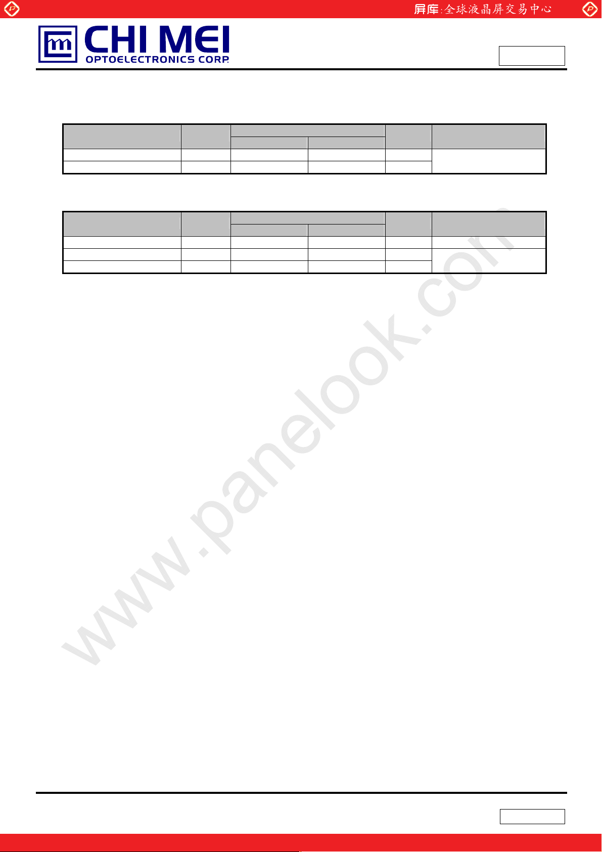
Note (2) Measurement Conditions:
Value
Unit Note
+5.0V
R1
47K
Q1 2SK1475
FUSE
C3
1uF
Vcc
(LCD Module Input)
(High to Low)
(Control Signal)
SW
+12V
C1
1uF
VR1
R2
1K
47K
0.01uF
Q2
2SK1470
C2
Vcc rising time is 470Ps
+5.0V
0.9Vcc
0.1Vcc
GND
470Ps
7 / 30
One step solution for LCD / PDP / OLED panel application: Datasheet, inventory and accessory!
Version 3.0
www.panelook.com
Page 8
Global LCD Panel Exchange Center
Issued Date: Feb. 26, 2007
www.panelook.com
Doc No.:
Model No.: M240J1-L03
Approval
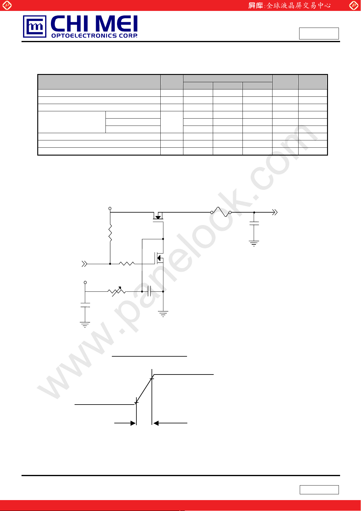
Note (3) The specified power supply current is under the conditions at Vcc = 5.0 V, Ta = 25 ± 2 ºC, fv = 60
Hz, whereas a power dissipation check pattern below is displayed.
a. White Pattern
Active Area
c. Vertical Stripe Pattern
b. Black Pattern
Active Area
R
G
R
B
G
R
B
G
R R
G
B
B
B
B
R
R
R
G
G
G
G
B
B
B
B
R
R
Active Area
8 / 30
One step solution for LCD / PDP / OLED panel application: Datasheet, inventory and accessory!
Version 3.0
www.panelook.com
Page 9
Global LCD Panel Exchange Center
)
)
)
(
)
Issued Date: Feb. 26, 2007
www.panelook.com
Doc No.:
Model No.: M240J1-L03
Approval
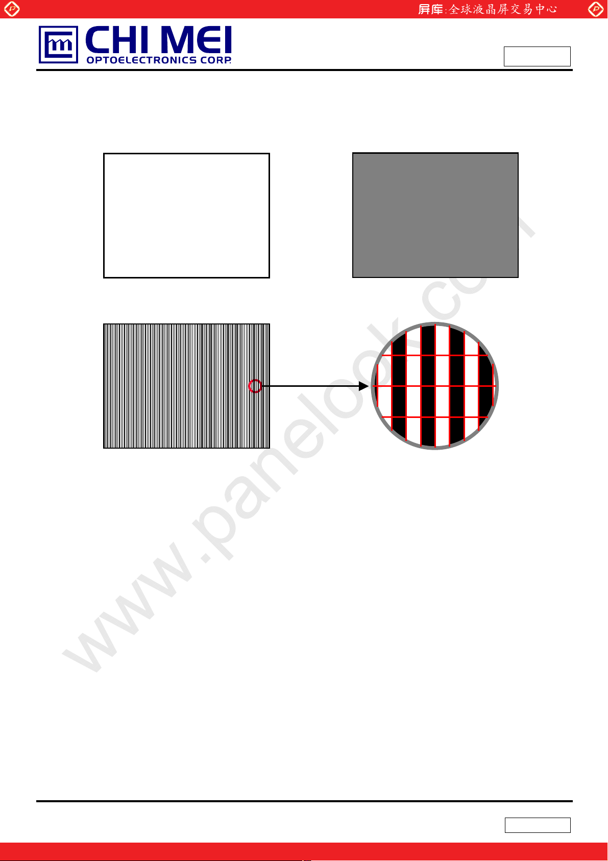
4. BLOCK DIAGRAM
4.1 TFT LCD MODULE
RXO0(+/-)
RXO1(+/-)
RXO2(+/-)
RXO3(+/-)
RXOC(+/-)
RXE0(+/-)
RXE1(+/-)
RXE2(+/-)
RXE3(+/-)
RXEC(+/-)
NC
Vcc
GND
(Starconn 093G30-B0001A
or JAE FI-X30SSL-HF)
INPUT CONNECTOR
TIMING CONTROLLER
DC/DC CONVERTER &
REFERENCE VOLTAGE
LVDS INPUT /
SCAN DRIVER IC
TFT LCD PANEL
(1920x3x1200)
DATA DRIVER IC
VL
(YEONHO 20015HS-04LB)
4.2 BACKLIGHT UNIT
LAMP CONNECTOR
BACKLIGHT UNIT
HV (+
HV (-
.
.
.
.
HV (+
9 / 30
One step solution for LCD / PDP / OLED panel application: Datasheet, inventory and accessory!
HV
-
Version 3.0
www.panelook.com
Page 10

Global LCD Panel Exchange Center
Issued Date: Feb. 26, 2007
www.panelook.com
Doc No.:
Model No.: M240J1-L03
Approval
5. INPUT TERMINAL PIN ASSIGNMENT
5.1 TFT LCD MODULE
Pin Name Description
1 RXO0- Negative LVDS differential data input. Channel O0 (odd)
2 RXO0+ Positive LVDS differential data input. Channel O0 (odd)
3 RXO1- Negative LVDS differential data input. Channel O1 (odd)
4 RXO1+ Positive LVDS differential data input. Channel O1 (odd)
5 RXO2- Negative LVDS differential data input. Channel O2 (odd)
6 RXO2+ Positive LVDS differential data input. Channel O2 (odd)
7 GND Ground
8 RXOC- Negative LVDS differential clock input. (odd)
9 RXOC+ Positive LVDS differential clock input. (odd)
10 RXO3- Negative LVDS differential data input. Channel O3(odd)
11 RXO3+ Positive LVDS differential data input. Channel O3 (odd)
12 RXE0- Negative LVDS differential data input. Channel E0 (even)
13 RXE0+ Positive LVDS differential data input. Channel E0 (even)
14 GND Ground
15 RXE1- Negative LVDS differential data input. Channel E1 (even)
16 RXE1+ Positive LVDS differential data input. Channel E1 (even)
17 GND Ground
18 RXE2- Negative LVDS differential data input. Channel E2 (even)
19 RXE2+ Positive LVDS differential data input. Channel E2 (even)
20 RXEC- Negative LVDS differential clock input. (even)
21 RXEC+ Positive LVDS differential clock input. (even)
22 RXE3- Negative LVDS differential data input. Channel E3 (even)
23 RXE3+ Positive LVDS differential data input. Channel E3 (even)
24 GND Ground
25 NC No connection
26 NC Not connection.
27 VCC +5.0V power supply
28 VCC +5.0V power supply
29 VCC +5.0V power supply
30 VCC +5.0V power supply
Note (1) Connector Part No.: Starconn 093G30-B0001A or JAE FI-X30SSL-HF.
Note (2) The first pixel is odd.
Note (3) Input signal of even and odd clock should be the same timing.
10 / 30
Version 3.0
One step solution for LCD / PDP / OLED panel application: Datasheet, inventory and accessory!
www.panelook.com
Page 11

Global LCD Panel Exchange Center
Issued Date: Feb. 26, 2007
www.panelook.com
Doc No.:
Model No.: M240J1-L03
Approval
SELLVDS = Low or Open
LVDS Channel E0
LVDS Channel E1
LVDS Channel E2
LVDS Channel E3
LVDS Channel O0
LVDS Channel O1
LVDS Channel O2
LVDS Channel O3
LVDS output D7 D6 D4 D3 D2 D1 D0
Data order EG0 ER5 ER4 ER3 ER2 ER1 ER0
LVDS output D18 D15 D14 D13 D12 D9 D8
Data order EB1 EB0 EG5 EG4 EG3 EG2 EG1
LVDS output D26 D25 D24 D22 D21 D20 D19
Data order DE NA NA EB5 EB4 EB3 EB2
LVDS output D23 D17 D16 D11 D10 D5 D27
Data order NA EB7 EB6 EG7 EG6 ER7 ER6
LVDS output D7 D6 D4 D3 D2 D1 D0
Data order OG0 OR5 OR4 OR3 OR2 OR1 OR0
LVDS output D18 D15 D14 D13 D12 D9 D8
Data order OB1 OB0 OG5 OG4 OG3 OG2 OG1
LVDS output D26 D25 D24 D22 D21 D20 D19
Data order DE NA NA OB5 OB4 OB3 OB2
LVDS output D23 D17 D16 D11 D10 D5 D27
Data order NA OB7 OB6 OG7 OG6 OR7 OR6
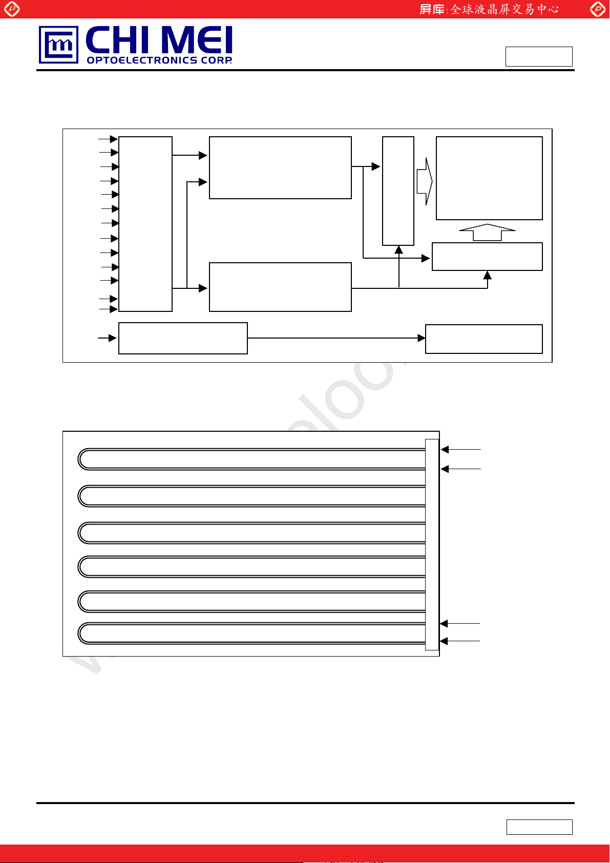
5.2 BACKLIGHT UNIT:
Pin Symbol Description Remark
1-1 HV High Voltage Pink
1-2 HV High Voltage White
2-3 HV High Voltage Pink
2-4 HV High Voltage White
3-5 HV High Voltage Pink
3-6 HV High Voltage White
4-7 HV High Voltage Pink
4-8 HV High Voltage White
5-9 HV High Voltage Pink
5-10 HV High Voltage White
6-11 HV High Voltage Pink
6-12 HV High Voltage White
Note (1) Connector Part No.: 20015HS-04LB (YEONHO) or equivalent
11 / 30
One step solution for LCD / PDP / OLED panel application: Datasheet, inventory and accessory!
Version 3.0
www.panelook.com
Page 12

Global LCD Panel Exchange Center
Issued Date: Feb. 26, 2007
www.panelook.com
Doc No.:
Model No.: M240J1-L03
Approval
5.3 COLOR DATA INPUT ASSIGNMENT
The brightness of each primary color (red, green and blue) is based on the 8-bit gray scale data input for
the color. The higher the binary input, the brighter the color. The table below provides the assignment of
color versus data input.
Data Signal
Basic
Colors
Gray
Scale
Of
Red
Color
Black
Red
Green
Blue
Cyan
Magenta
Yellow
White
Red(0) / Dark
Red(1)
Red(2)
Red(253)
Red(254)
Red(255)
R7 R6 R5 R4 R3 R2 R1 R0 R7 R6 G5 G4 G3 G2 G1 G0 R7 R6 B5 B4 B3 B2 B1 B0
0
0
1
1
0
0
0
0
0
0
1
1
1
1
1
1
0
0
0
0
0
0
:
:
:
:
:
:
1
1
1
1
1
1
Red Green Blue
0
0
0
0
0
0
0
0
0
0
0
0
0
0
0
0
0
0
0
0
1
1
1
1
1
1
0
0
0
0
0
0
0
0
0
0
0
0
0
0
0
0
0
0
0
0
1
1
1
1
1
1
1
1
0
0
0
0
0
0
0
0
0
0
0
0
0
0
0
0
0
0
0
0
1
1
1
1
1
1
0
0
0
0
0
0
1
1
1
1
1
1
1
1
1
1
1
1
1
1
1
1
1
1
1
1
0
0
0
0
0
0
0
0
1
1
1
1
1
1
1
1
1
1
1
1
1
1
1
1
1
1
1
1
0
0
0
0
0
0
1
1
1
1
1
1
1
1
1
1
1
1
1
1
1
1
1
1
1
1
0
0
0
0
0
0
0
0
0
0
0
0
0
0
0
0
0
0
0
0
0
0
0
0
0
1
0
0
0
0
0
0
0
0
0
0
0
0
0
0
0
0
0
0
1
0
0
0
0
0
0
0
0
0
0
0
0
0
0
0
:
:
:
:
:
:
:
:
:
:
:
:
:
:
:
:
:
:
:
:
:
:
:
:
:
:
:
:
:
:
:
:
:
:
:
:
:
:
:
:
1
1
1
1
0
1
0
0
0
0
0
0
0
0
0
0
0
0
0
0
1
1
1
1
1
0
0
0
0
0
0
0
0
0
0
0
0
0
0
0
1
1
1
1
1
1
0
0
0
0
0
0
0
0
0
0
0
0
0
0
0
0
0
0
0
0
1
1
1
1
1
1
0
0
1
1
0
0
0
0
0
0
:
:
:
:
0
0
0
0
0
0
Green(0) / Dark
Gray
Scale
Of
Green
Gray
Scale
Of
Blue
Note (1) 0: Low Level Voltage, 1: High Level Voltage
Green(1)
Green(2)
Green(253)
Green(254)
Green(255)
Blue(0) / Dark
Blue(1)
Blue(2)
Blue(253)
Blue(254)
Blue(255)
0
0
0
0
0
0
0
0
0
0
0
0
0
0
0
0
0
0
0
0
0
:
:
:
:
:
:
:
:
:
:
:
:
:
:
:
:
0
0
0
0
0
0
0
0
0
0
0
0
0
0
0
0
0
0
0
0
0
0
0
0
0
0
0
0
0
0
0
0
0
0
0
0
0
0
0
0
0
0
:
:
:
:
:
:
:
:
:
:
:
:
:
:
:
:
0
0
0
0
0
0
0
0
0
0
0
0
0
0
0
0
0
0
0
0
0
0
0
0
0
0
0
0
0
0
0
0
0
0
0
0
0
0
0
0
0
0
0
0
0
0
1
0
0
0
0
0
0
0
0
0
0
0
0
0
0
0
1
0
0
0
0
0
0
0
0
0
:
:
:
:
:
:
:
:
:
:
:
:
:
:
:
:
:
:
:
:
:
:
:
:
:
:
:
:
:
:
:
:
:
:
0
1
1
1
1
1
1
0
1
0
0
0
0
0
0
0
0
0
1
1
1
1
1
1
1
0
0
0
0
0
0
0
0
0
0
1
1
1
1
1
1
1
1
0
0
0
0
0
0
0
0
0
0
0
0
0
0
0
0
0
0
0
0
0
0
0
0
0
0
0
0
0
0
0
0
0
0
0
0
0
0
0
0
0
1
0
0
0
0
0
0
0
0
0
0
0
0
0
0
0
1
0
:
:
:
:
:
:
:
:
:
:
:
:
:
:
:
:
:
:
:
:
:
:
:
:
:
:
:
:
:
:
:
:
:
:
0
0
0
0
0
0
0
0
0
1
1
1
1
1
1
0
1
0
0
0
0
0
0
0
0
0
1
1
1
1
1
1
1
0
0
0
0
0
0
0
0
0
0
1
1
1
1
1
1
1
1
12 / 30
One step solution for LCD / PDP / OLED panel application: Datasheet, inventory and accessory!
Version 3.0
www.panelook.com
Page 13

Global LCD Panel Exchange Center
Issued Date: Feb. 26, 2007
www.panelook.com
Doc No.:
Model No.: M240J1-L03
Approval
6. INVERTER SPECIFICATIONS
6.1 CONNECTOR TYPE
Items Input connector type Output connector type
CN1 YEONHO 20022WR-14L YEONHO 20022HS-14L
CN2 ACES 88260-02001-06 ACES 87214-0200
CAN-CNE YEONHO 20015HS-04LB YEONHO 20015WR-07B
6.2 INPUT CONNECTOR PIN ASSIGNMENT
CN1 : YEONHO 20022WR-14L
No. Signal Feature
1
2
+24 V
3
4
5
V
BL
6
7
8
9
10
11 SOS Shutdown Protection Signal
12 BLON BL ON/OFF
13 ADIM Analog Mode Dimming
14 SCAN ON/OFF SCAN BL ON/OFF
CN2 : ACES 88260-02001-06
No. Signal Feature
1 STV STV Signal Input
2 GND GND
6.3 OUTPUT CONNECTOR PIN ASSIGNMENT
CNA-CNE : YEONHO 20015WR-07B
No. Signal Feature
1 CFL HOT CFL High Voltage
2 CFL HOT CFL High Voltage
GND GND
13 / 30
One step solution for LCD / PDP / OLED panel application: Datasheet, inventory and accessory!
Version 3.0
www.panelook.com
Page 14

Global LCD Panel Exchange Center
www.panelook.com
Doc No.:
Issued Date: Feb. 26, 2007
Model No.: M240J1-L03
Approval
6.4 GENERAL ELECTRICAL SPECIFICATIONS
6.4.1 ABSOLUTE MAXIMUM RATING
NO. ITEM SYMBOL
TEST
CONDITION
MIN. TYP. MAX. UNIT NOTE
(1)
1 INPUT VOLTAGE VIN - 0 - 28 V
SHUTDOWN PROTECTION
2
SIGNAL
3 ON/OFF CONTROL VOLTAGE V
4 ANALOG DIMMING VOLTAGE V
SCAN MODE ON/OFF
5
CONTROL VOLTAGE
6 STV SIGNAL V
7 OPERATING TEMPERATURE TOP 5~90% RH 0 - 75 °C
8 STORAGE TEMPERATURE TST 5~95% RH -30 - 80 °C
SOS -
-
BLON
-
ADIM
-
V
SCAN
-
STV
-0.5 - 6.5 V
Protect
inverters from
moisture
condensation
and freezing.
(Note 1)
Note: The absolute maximum rating that a rated value must not be exceeded during operation. When it is used
exceeding the maximum rating, for a certain reason, a possibility that an inverter may be damaged also
recommends being used fully in operating condition as below.
6.4.2 OPERATING CONDITION
NO. ITEM SYMBOL
TEST
CONDITION
MIN. TYP. MAX. UNIT NOTE
1 POWER CONSUMPTION PBL Normal mode - - 72 W
(1)
2 INPUT VOLTAGE VBL - 21.6 24 26.4 V
3 INPUT CURRENT IIN - - 3 3.5 A
SHUTDOWN PROTECTION
4
SIGNAL
5 ON/OFF CONTROL VOLTAGE V
6 ANALOG DIMMING VOLTAGE V
SCAN MODE ON/OFF
7
CONTROL VOLTAGE
8 STV SIGNAL T
SOS
BLON
ADIM
V
SCAN
STV
9 OPERATING TEMPERATURE TOP
10 STORAGE TEMPERATURE TST
Normal - 0 - V
Abnormal - 5 - V
V
=ON 2.5 - 5 V
BLON
V
=OFF 0 - 0.8 V
BLON
Max. - 5 - V
Min. - 0 - V
V
=H 2.5 - 5 V
SCAN
V
=L 0 - 0.8 V
SCAN
V
=H 2.5 - 5 V
SYN
V
=L 0 - 0.8 V
SYN
20Д95% RH
5Д95% RH
0 - 60 °C
-20 - 75 °C
Protect
inverters from
moisture
condensation
and freezing.
(Note 1)
Note 1 Temperature and relative humidity condition are as below.
(a) 90 %RH Max. (Ta Љ 40 C)
(b) Wet-bulb temperature should be 39 ºC Max. (Ta > 40 ºC).
(c) No condensation of water.
14 / 30
One step solution for LCD / PDP / OLED panel application: Datasheet, inventory and accessory!
Version 3.0
www.panelook.com
Page 15

Global LCD Panel Exchange Center
www.panelook.com
Doc No.:
Issued Date: Feb. 26, 2007
Model No.: M240J1-L03
Approval
6.4.3 INITIAL CHARACTERISTICS (Ta = 25 5 °C)
NO. ITEM SYMBOL
1 INPUT VOLTAGE VBL - 21.6 24 26.4 V
2 INPUT CURRENT IBL Normal Mode - 3 3.5 A
3 INPUT INRUSH CURRENT - VBL=24 V - - 6 A
INDIVIDUAL MAXIMUM LAMP
4
CURRENT
SCAN MODE INDIVIDUAL
5
LAMP CURRENT
6 OSCILLATING FREQUENCY FW - 50 55 70 KHz
7 BURST MODE FREQUENCY FB Normal Mode - 180 - Hz
8 OPEN LAMP VOLTAGE VS
9 LAMP VOLTAGE VW Ta=25 °C - 1900 - V
10 RISING TIME T
11 FALLING TIME T
12 START-UP TIME TS 0.9*IЊ
I
L(max.)
I
L(min.)
- - - 500 μs
RISE
- - - 500 μs
FAL L
TEST
CONDITION
Normal Mode
or
Scan Mode
Scan Mode
or
Scan Mode
Ta=0 °C 3900 - - V
Ta=25 °C 3670 - - V
MIN. TYP. MAX. UNIT NOTE
10.4 - 11.4 mA
2.7 - 3.7 mA
1 - 2 Sec.
L
peak
rms
rms
rms
See Fig. 1,
(Note 3)
Power on to IL
stabilize period
13 TOTAL EFFICIENCY - 80 - - %
PBL / PL, (Load:
CCFL)
Note 2 Lamp for measurement, use back light: 24”back light unit. The measurement result is a result
after 30 minutes of lighting.
Note 3 The definitions of rising time, falling time and remains current are based on high side lamp
current and diagramed as Fig.1.
15 / 30
One step solution for LCD / PDP / OLED panel application: Datasheet, inventory and accessory!
Version 3.0
www.panelook.com
Page 16

Global LCD Panel Exchange Center
www.panelook.com
Doc No.:
Issued Date: Feb. 26, 2007
Model No.: M240J1-L03
Approval
6.4.4 PROTECTION CHARACTERISTICS
NO. ITEM TEST CONDITION
OPEN LAMP PROTECTION
1
(OLP)
OUTPUT SHORT PROTECTION
2
(OSP)
INPUT OVER VOLTAGE PROTECTION
3
(IOP)
INPUT UNDER VOLTAGE PROTECTION
4
(IUP)
Note 4 T
Output Shutter: 2 K
Њ1.25*Vin (typ)
is the duration since inverter ignition till shutdown by protection circuit is triggered.
fault
- Shutdown
Љ0.8*Vin (typ)
RESPONDENCE OF
SUBJECT
Shutdown or
I
(peak value)Љ
short
2.8*I
rms
Shutdown
Shutdown
NOTE
1S<T
fault
(Note 4~7)
Note 5 Any output short outside inverter should be protected.
Note 6 Whatever the above items occurred before inverter turn on or under inverter operating
duration that inverter should be protected.
Note 7 When OLP & OSP protections have been trigged, inverter shall be restarted by input power
source and V
BLON
signal.
6.4.5 INTERFACE CHARACTERISTICS
NO. ITEM SYMBOL
TEST
CONDITION
MIN. TYP. MAX. UNIT NOTE
<2S
(11-12)
ON/OFF CONTROL
1
VOLTAGE
ANALOG DIMMING
2
VOLTAGE
SCAN MODE
3
CONTROL VOLTAGE
4 STV SINGLE VOLTAGE
ON - 2.5 - 5 V
V
BLON
OFF
MAX - - - 5 V
V
ADIM
MIN
ON - 2.5 - 5 V
V
SCAN
OFF
HI - 2.5 - 5 V
V
STV
LO
- 0 - 0.8 V
- - 0 - V
- 0 - 0.8 V
- 0 - 0.8 V
Minimum
Duty
Ratio
Maximum
Duty
Ratio
Ext. Dim.
Control
Int. Dim.
Control
Note 8 Even if control signal over range in any conditions that there must no smell, smoke, and fire
cause by any failure on inverter PCB or components.
Note 9 All the interface circuits without spike suppress component hence the hot plug in or plug out
of all connectors are inhibited.
16 / 30
One step solution for LCD / PDP / OLED panel application: Datasheet, inventory and accessory!
Version 3.0
www.panelook.com
Page 17

Global LCD Panel Exchange Center
www.panelook.com
Doc No.:
Issued Date: Feb. 26, 2007
Model No.: M240J1-L03
Approval
6.4.6 Inverter Operating Mode
ON/OFF CONTROL
VBLON
No O PERAT I N G STATU S
1 INVERTER OFF - - DISABLE
2
3
4
NORMAL MODE
OPERATIONʳ
SCAN MODE
OPERTAION
PROTECTION MODE
OPERATION(NOTE 10)
ON OFF MAX. MIN. ON OFF ENABLE DISABLE
2.5~5V 0~0.8V 5V 0V 2.5~5V 0~0.8V 2.5~5V 0~0.8V
V - ENABLE - V V -
V - ENABLE V - V -
V - DISABLE
ANALOG DIMMING
VADIM.
SCAN MODE
CONTROL
VSCAN
DON’T
CARE
DON’T
CARE
DON’T
CARE
DON’T
CARE
STV SINGLE INPUT
VSTV
DON’T
CARE
- V
DON’T
CARE
17 / 30
One step solution for LCD / PDP / OLED panel application: Datasheet, inventory and accessory!
Version 3.0
www.panelook.com
Page 18

Global LCD Panel Exchange Center
Issued Date: Feb. 26, 2007
www.panelook.com
Doc No.:
Model No.: M240J1-L03
Approval
7. INTERFACE TIMING
7.1 INPUT SIGNAL TIMING SPECIFICATIONS
The input signal timing specifications are shown as the following table and timing diagram.
Signal Item Symbol Min. Typ. Max. Unit Note
Frequency Fc 50.0 77 83.0 MHz -
LVDS Clock
LVDS Da t a
Vertical Active Display Term
Horizontal Active Display Term
Note: Because this module is operated by DE only mode, Hsync and Vsync input signals should be set
Period Tc - 13.0 - ns
High Time Tch - 4/7 - Tc Low Time Tcl - 3/7 - Tc Setup Time Tlvs 600 - - ps Hold Time Tlvh 600 - - ps Frame Rate Fr 40 60 63 Hz Tv=Tvd+Tvb
Total Tv 1209 1235 1245 Th Display Tvd 1200 1200 1200 Th Blank Tvb (9) 35 Tv-Tvd Th Total Th 1030 1040 1075 Tc Th=Thd+Thb
Display Thd 960 960 960 Tc Blank Thb 70 80 Th-Thd Tc -
to low logic level or ground. Otherwise, this module would operate abnormally.
INPUT SIGNAL TIMING DIAGRAM
DE
Th
DCLK
T
C
DE
DATA
Thb
hd
T
18 / 30
One step solution for LCD / PDP / OLED panel application: Datasheet, inventory and accessory!
Version 3.0
www.panelook.com
Page 19

Global LCD Panel Exchange Center
www.panelook.com
Doc No.:
Issued Date: Feb. 26, 2007
Model No.: M240J1-L03
Approval
7.2 POWER ON/OFF SEQUENCE
To prevent a latch-up or DC operation of LCD module, the power on/off sequence should be as the
diagram below.
Restart
Power On
Power Off
Power Supply
for LCD, Vcc
- Interface Signal
(LVDS Signal of
Transmitter), V
- Power for Lamp
Timing Specifications:
0.5< t1 Љ 10 msec
0 < t2 Љ 50 msec
0 < t3 Љ 50 msec
0V
0V
I
t4 Њ 500 msec
t5 Њ 500 msec
10%
90%
90%
10%
t1
t4
t3 t2
Valid Data
t6 t5
50%50%
ONOFF OFF
t6 Њ 90 msec
19 / 30
One step solution for LCD / PDP / OLED panel application: Datasheet, inventory and accessory!
Version 3.0
www.panelook.com
Page 20

Global LCD Panel Exchange Center
www.panelook.com
Doc No.:
Issued Date: Feb. 26, 2007
Model No.: M240J1-L03
Approval
8. OPTICAL CHARACTERISTICS
8.1 TEST CONDITIONS
Item Symbol Value Unit
Ambient Temperature Ta
Ambient Humidity Ha
25r2
50r10
Supply Voltage VCC 5.0 V
Input Signal According to typical value in "3. ELECTRICAL CHARACTERISTICS"
Lamp Current IL (6.0) mA
Inverter Operating Frequency FL 50 KHz
Inverter BSVD24U01A
8.2 OPTICAL SPECIFICATIONS
The relative measurement methods of optical characteristics are shown in 7.2. The following items should
be measured under the test conditions described in 7.1 and stable environment shown in Note (5).
o
C
%RH
Item Symbol Condition Min. Typ. Max. Unit Note
Red
Color
Green
Chromaticity
(CIE 1931)
Blue
White
Center Luminance of White
(Center of Screen)
Contrast Ratio CR
Response Time
Motion Picture Response Time
(For Scan Function)
White Variation
Horizontal
Viewing Angle
Vertica l
Rx
Ry
Gx
Gy
Bx
By
Wx
Wy
L
C
=0q, TY =0q
T
x
CS-1000T
Typ -
0.03
350 400 - cd/m2(4), (5)
0.640
0.348
0.293
0.585
0.143
0.075
0.313
0.329
Typ +
0.03
- (1), (5)
700 1000 - - (2), (5)
TR - 13 18
TF - 7 12
T
GtoG,AVE
Tx=0q, TY =0q
- 8 13
ms (3),(7)
Off - 19 -
T
MPRT
T
=0q, TY =0q
x
ms (8)
On - 14 -
GW T
Tx+
-
T
x
TY+
T
-
Y
=0q, TY =0q
x
CR Њ 10
- 1.25 1.40 - (5), (6)
80 88 80 88 80 88 -
Deg. (1), (5)
80 88 -
20 / 30
One step solution for LCD / PDP / OLED panel application: Datasheet, inventory and accessory!
Version 3.0
www.panelook.com
Page 21

Global LCD Panel Exchange Center
y
y
y
www.panelook.com
Doc No.:
Issued Date: Feb. 26, 2007
Model No.: M240J1-L03
Approval
Note (1) Definition of Viewing Angle (Tx, Ty):
Normal
TX- = 90º
6 o’clock
T
- = 90º
x-
y-
Note (2) Definition of Contrast Ratio (CR):
The contrast ratio can be calculated by the following expression.
Contrast Ratio (CR) = L255 / L0
L255: Luminance of gray level 255
L 0: Luminance of gray level 0
Tx = T
= 0º
Ty- Ty
Tx
Tx
12 o’clock direction
y+
T
+ = 90º
x+
TX+ = 90º
CR = CR (1)
CR (X) is corresponding to the Contrast Ratio of the point X at Figure in Note (6).
Note (3) Definition of Response Time (T
100%
90%
Optical
Response
Gray Level 255
10%
0%
, TF):
R
Gray Level 255
Gray Level 0
T
F
T
R
66.67ms 66.67ms
21 / 30
One step solution for LCD / PDP / OLED panel application: Datasheet, inventory and accessory!
Version 3.0
www.panelook.com
Page 22

Global LCD Panel Exchange Center
Issued Date: Feb. 26, 2007
www.panelook.com
Doc No.:
Model No.: M240J1-L03
Approval
Note (4) Definition of Luminance of White (LC):
Measure the luminance of gray level 255 at center point
LC = L (1)
L (x) is corresponding to the luminance of the point X at Figure in Note (6).
Note (5) Measurement Setup:
The LCD module should be stabilized at given temperature for 40 minutes to avoid abrupt
temperature change during measuring. In order to stabilize the luminance, the measurement
should be executed after lighting Backlight for 40 minutes in a windless room.
LCD Module
LCD Panel
USB2000
Center of the Screen
CS-1000T
Light Shield Room
(Ambient Luminance < 2 lux)
22 / 30
One step solution for LCD / PDP / OLED panel application: Datasheet, inventory and accessory!
Version 3.0
www.panelook.com
Page 23

Global LCD Panel Exchange Center
X
A
Issued Date: Feb. 26, 2007
www.panelook.com
Doc No.:
Model No.: M240J1-L03
Approval
Note (6) Definition of White Variation (GW):
Measure the luminance of gray level 255 at 13 points
GW =
Maximum [L(1), L(2), L(3), L(4), L(5), L(6), L(7), L(8), L(9), L(10), L(11), L(12), L(13)]
Minimum [L(1), L(2), L(3), L(4), L(5), L(6), L(7), L(8), L(9), L(10), L(11), L(12), L(13)]
Horizontal Line Number
˄˃
Vertical Line Number
ˉ
˛˂ˇ
˅
˛
ˌ
ˊ
ˆ
˄
ˋ
˄˃
ΚTest Point
XЈ1 to 13
ˇˈ
˛˂ˇ ˛˂ˇ ˛˂ˇ
˄˄ ˄˅
˄˃ ˄˃
˄˃
˪˂ˇ ˪˂ˇ ˪˂ˇ ˪˂ˇ
˪
˄ˆ
ctive Area
Note (7) Definition of Response Time (T
T
The Gray to Gray response time is defined as the following chart.
Initial Gray
GTG_AVE
Gray to Gray
is defined as the total average response time for “Gray To Gray “.
G0
G32
G64
G96
G128
G160
G192
G224
G255
GTG_AVE
G0 G32 G64 G96 G128 G160 G192 G224 G255
):
Target Gray
23 / 30
Version 3.0
One step solution for LCD / PDP / OLED panel application: Datasheet, inventory and accessory!
www.panelook.com
Page 24

Global LCD Panel Exchange Center
Issued Date: Feb. 26, 2007
www.panelook.com
Doc No.:
Model No.: M240J1-L03
Approval
Note (8) Definition of MPRT (T
The motion picture response time (in mini-second) is the average of
blurred edge widths divided by scroll speed u (10 pixels per frame):
T
uNf
where
b
is 10% to 90% blurred edge width measured by Otsuka MPRT-1000.
ij
f is frame rate.
N is the number of iЋj transitions. For the case of nine gray levels ( i = 0, 31, 63, 91, 127, 191, 223,
255; j = 0, 31, 63, 91, 127, 191, 223, 255, and iЋj).
MPRT
1
b
¦
ijMPRT
z ji
LCD Module
LCD Panel
):
Ostuka
MPRT-1000
The width of measurement area >100 pixels
Light Shield Room
(Ambient Luminance < 2 lux)
24 / 30
One step solution for LCD / PDP / OLED panel application: Datasheet, inventory and accessory!
Version 3.0
www.panelook.com
Page 25

Global LCD Panel Exchange Center
Issued Date: Feb. 26, 2007
www.panelook.com
Doc No.:
Model No.: M240J1-L03
Approval
9. PACKAGING
9.1 PACKING SPECIFICATIONS
(1) 5 LCD modules / 1 Box
(2) Box dimensions: 645(L) X 377(W) X 470(H) mm
(3) Weight: approximately 17.5Kg (5 modules per box)
9.2 PACKING METHOD
(1) Carton Packing should have no failure in the following reliability test items.
Test Item Test Conditions Note
ISTA STANDARD
Random, Frequency Range: 1 – 200 Hz
Vibration
Dropping Test 1 Angle, 3 Edge, 6 Face, 60cm Non Operation
Top & Bottom: 30 minutes (+Z), 10 min (-Z),
Right & Left: 10 minutes (X)
Back & Forth 10 minutes (Y)
Non Operation
Figure. 9-1 Packing method
For ocean shipping
25 / 30
One step solution for LCD / PDP / OLED panel application: Datasheet, inventory and accessory!
Version 3.0
www.panelook.com
Page 26

Global LCD Panel Exchange Center
Issued Date: Feb. 26, 2007
www.panelook.com
Doc No.:
Model No.: M240J1-L03
Approval
For air transport
Figure. 9-2 Packing method
Figure. 9-3 Packing method
10. DEFINITION OF LABELS
26 / 30
One step solution for LCD / PDP / OLED panel application: Datasheet, inventory and accessory!
Version 3.0
www.panelook.com
Page 27

Global LCD Panel Exchange Center
ˤ˟˗˃ˇˉˉˀ˃˃˅
Issued Date: Feb. 26, 2007
www.panelook.com
Doc No.:
Model No.: M240J1-L03
Approval
10.1 CMO MODULE LABEL
The barcode nameplate is pasted on each module as illustration, and its definitions are as following explanation.
(a) Model Name: M240J1-L03
(b) Revision: Rev. XX, for example: A0, A1… B1, B2… or C1, C2…etc.
(c) CMO barcode definition:
Serial ID: XX
Code Meaning Description
XX CMO internal use -
XX Revision Cover all the change
X CMO internal use -
XX CMO internal use -
YMD Year, month, day
L Product line # Line 1=1, Line 2=2, Line 3=3, …
NNNN Serial number Manufacturing sequence of product
(d) Customer’s barcode definition:
Serial ID:
-XX-X-XX-YMD-L-NNNN
Year: 2001=1, 2002=2, 2003=3, 2004=4…
Month: 1~12=1, 2, 3, ~, 9, A, B, C
Day: 1~31=1, 2, 3, ~, 9, A, B, C, ~, W, X, Y, exclude I, O, and U.
11. PRECAUTIONS
11.1 ASSEMBLY AND HANDLING PRECAUTIONS
(1) Do not apply rough force such as bending or twisting to the module during assembly.
(2) To assemble or install module into user’s system can be only in clean working areas. The dust and oil
may cause electrical short or worsen the polarizer.
(3) It’s not permitted to have pressure or impulse on the module because the LCD panel and Backlight will
be damaged.
(4) Always follow the correct power sequence when LCD module is connecting and operating. This can
prevent damage to the CMOS LSI chips during latch-up.
(5) Do not pull the I/F connector in or out while the module is operating.
(6) Do not disassemble the module.
(7) Use a soft dry cloth without chemicals for cleaning, because the surface of polarizer is very soft and
easily scratched.
(8) It is dangerous that moisture come into or contacted the LCD module, because moisture may damage
27 / 30
One step solution for LCD / PDP / OLED panel application: Datasheet, inventory and accessory!
Version 3.0
www.panelook.com
Page 28

Global LCD Panel Exchange Center
Issued Date: Feb. 26, 2007
www.panelook.com
Doc No.:
Model No.: M240J1-L03
Approval
LCD module when it is operating.
(9) High temperature or humidity may reduce the performance of module. Please store LCD module within
the specified storage conditions.
(10) When ambient temperature is lower than 10ºC may reduce the display quality. For example, the
response time will become slowly, and the starting voltage of CCFL will be higher than room
temperature.
11.2 SAFETY PRECAUTIONS
(1) The startup voltage of Backlight is approximately 1000 Volts. It may cause electrical shock while
assembling with inverter. Do not disassemble the module or insert anything into the Backlight unit.
(2) If the liquid crystal material leaks from the panel, it should be kept away from the eyes or mouth. In
case of contact with hands, skin or clothes, it has to be washed away thoroughly with soap.
(3) After the module’s end of life, it is not harmful in case of normal operation and storage.
28 / 30
One step solution for LCD / PDP / OLED panel application: Datasheet, inventory and accessory!
Version 3.0
www.panelook.com
Page 29

www.panelook.com
www.panelook.com
Global LCD Panel Exchange Center
One step solution for LCD / PDP / OLED panel application: Datasheet, inventory and accessory!
Page 30

www.panelook.com
www.panelook.com
Global LCD Panel Exchange Center
One step solution for LCD / PDP / OLED panel application: Datasheet, inventory and accessory!
 Loading...