

Page 1

Global LCD Panel Exchange Center
www.panelook.com
One step solution for LCD / PDP / OLED panel application: Datasheet, inventory and accessory!
www.panelook.com
Page 2
Global LCD Panel Exchange Center
REVISION HISTORY
1. GENERAL DESCRIPTION
1.1 OVERVIEW
1.2 FEATURES
1.3 APPLICATION
1.4 GENERAL SPECIFICATIONS
1.5 MECHANICAL SPECIFICATIONS
2. ABSOLUTE MAXIMUM RATINGS
2.1 ABSOLUTE RATINGS OF ENVIRONMENT
2.2 ELECTRICAL ABSOLUTE RATINGS
2.2.1 TFT LCD MODULE
2.2.2 BACKLIGHT UNIT
3. ELECTRICAL CHARACTERISTICS
3.1 TFT LCD MODULE
3.2 BACKLIGHT UNIT
4. BLOCK DIAGRAM
4.1 TFT LCD MODULE
4.2 BACKLIGHT UNIT
5. INPUT TERMINAL PIN ASSIGNMENT
5.1 TFT LCD MODULE
5.2 LVDS DATA ASSIGNMENT
5.3 BACKLIGHT UNIT
5.4 COLOR DATA INPUT ASSIGNMENT
6. INTERFACE TIMING
6.1 INPUT SIGNAL TIMING SPECIFICATIONS
6.2 POWER ON/OFF SEQUENCE
7. OPTICAL CHARACTERISTICS
7.1 TEST CONDITIONS
7.2 OPTICAL SPECIFICATIONS
8. PRECAUTIONS
8.1 ASSEMBLY AND HANDLING PRECAUTIONS
8.2 SAFETY PRECAUTIONS
9. MODULE DRAWINGS
www.panelook.com
Issued Date: Dec. 26, 2002
Model No.: M201U3 - L01
Tentative
- CONTENTS -
------------------------------------------------------- 3
------------------------------------------------------- 4
------------------------------------------------------- 5
------------------------------------------------------- 6
------------------------------------------------------- 8
------------------------------------------------------- 9
------------------------------------------------------- 12
------------------------------------------------------- 15
------------------------------------------------------- 19
------------------------------------------------------- 20
2 / 21
The information described in this technical specification is tentative and it is possible to be changed without prior
notice. Please contact CMO ’s representative while your product design is based on this specification.
One step solution for LCD / PDP / OLED panel application: Datasheet, inventory and accessory!
Version 0.0
www.panelook.com
Page 3
Global LCD Panel Exchange Center
www.panelook.com
Issued Date: Dec. 26, 2002
Model No.: M201U3 - L01
Tentative
Version Date
Ver 0.0 Dec.26,’02 All
Page
(New)
REVISION HISTORY
Section Description
All Tentative Specification was first issued.
3 / 21
The information described in this technical specification is tentative and it is possible to be changed without prior
notice. Please contact CMO ’s representative while your product design is based on this specification.
One step solution for LCD / PDP / OLED panel application: Datasheet, inventory and accessory!
Version 0.0
www.panelook.com
Page 4
Global LCD Panel Exchange Center
1. GENERAL DESCRIPTION
1.1 OVERVIEW
M201U3 - L01 is a 20.1” TFT Liquid Crystal Display module with a 6-CCFL backlight unit and a 2ch-LVDS
interface. This module supports 1600 x 1200 UXGA mode and can display 16.7M colors. The inverter
module for Backlight is not built in.
1.2 FEATURES
- Wide viewing angle
- High contrast ratio
- Fast response time
- High color saturation
- UXGA (1600 x 1200 pixels) resolution
www.panelook.com
Issued Date: Dec. 26, 2002
Model No.: M201U3 - L01
Tentative
- DE (Data Enable) only mode
- LVDS (Low Voltage Differential Signaling) interface
1.3 APPLICATION
- TFT LCD Monitor
1.4 GENERAL SPECIFICATI0NS
Item Specification Unit Note
Active Area 408.0(H) x 306.0 (V) (20.1” diagonal) mm
Bezel Opening Area 413.0 (H) x 311.0 (V) mm
Driver Element a-si TFT active matrix - Pixel Number 1600 x R.G.B. x 1200 pixel Pixel Pitch 0.255 (H) x 0.255 (V) mm Pixel Arrangement RGB vertical stripe - Display Colors 16.7 M color Display Operation Mode Transmissive mode / Normally black - Surface Treatment Hard coating(2H), Anti-glare (Haze 25) - -
1.5 MECHANICAL SPECIFICATIONS
Item Min. Typ. Max. Unit Note
Horizontal(H) (431.5) 432.0 (432.5) mm
Module Size
Note (1) Please refer to the attached drawings for more information of front and back outline dimensions.
Vertical(V) (331.0) 331.5 (332.0) mm
Depth(D) TBD 25 mm
Weight (3700) TBD g -
(1)
(1), (2)
Note (2) Module Depth does not include connectors.
4 / 21
The information described in this technical specification is tentative and it is possible to be changed without prior
notice. Please contact CMO ’s representative while your product design is based on this specification.
One step solution for LCD / PDP / OLED panel application: Datasheet, inventory and accessory!
Version 0.0
www.panelook.com
Page 5
Global LCD Panel Exchange Center
2. ABSOLUTE MAXIMUM RATINGS
2.1 ABSOLUTE RATINGS OF ENVIRONMENT
Item Symbol
Storage Temperature TST -20 +60 ºC
Operation Ambient Temperature TOP 0 +45 ºC
Storage Humidity HST 5 85 %RH
Operation Humidity HOP 20 85 %RH
Shock (Non-Operation) (1) S
Vibration (Non-Operation) (2) V
Note (1) 30G, 6ms, 1time each ± X, ± Y, ± Z direction.
Note (2) 10 ~ 500 Hz, loctave / 20 minutes, 2G, 1.5mm max, 1 hour each X, Y, Z direction.
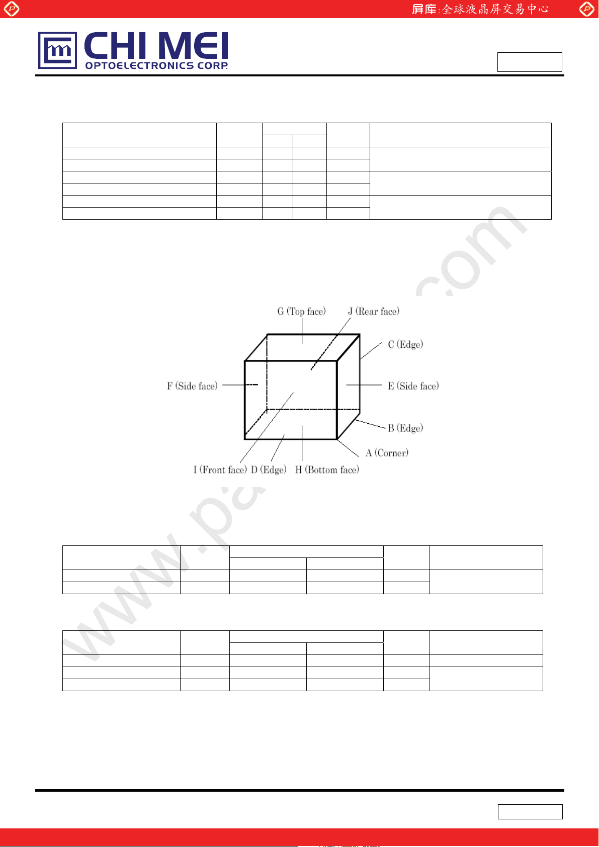
Note (3) Figure below shows the shock directions when module is packed. The shock resistance standards
are dropping location A ~J, dropping height 60 cm, and count 1 time for each direction.
www.panelook.com
Value
Min. Max.
- 30 G
NOP
- 2.0 G
NOP
Unit Note
Issued Date: Dec. 26, 2002
Model No.: M201U3 - L01
Tentative
Temperature on surface of LCD panel
(display area.)
Maximum wet-bulb temperature should
not exceed 29ºC. No condensation
For single module without package.
2.2 ELECTRICAL ABSOLUTE RATINGS
2.2.1 TFT LCD MODULE
Item Symbol
Power Supply Voltage Vcc -0.3 +14.0 V
Logic Input Voltage VIN -0.3 + 3.6 V
Min. Max.
Value
Unit Note
(1)
2.2.2 BACKLIGHT UNIT
Item Symbol
Lamp Voltage VL - (2.5K) V
Lamp Current IL - (6.5) MA
Lamp Frequency FL - (80) KHz
Note (1) Permanent damage to the device may occur if maximum values are exceeded. Function operation
should be restricted to the conditions described under Normal Operating Conditions.
Note (2) Specified values are for lamp (Refer to 3.2 for further information).
Min. Max.
Value
Unit Note
(1), (2), IL = 6.0 mA
RMS
RMS
(1), (2)
5 / 21
The information described in this technical specification is tentative and it is possible to be changed without prior
notice. Please contact CMO ’s representative while your product design is based on this specification.
One step solution for LCD / PDP / OLED panel application: Datasheet, inventory and accessory!
Version 0.0
www.panelook.com
Page 6
Global LCD Panel Exchange Center
www.panelook.com
Issued Date: Dec. 26, 2002
Model No.: M201U3 - L01
3. ELECTRICAL CHARACTERISTICS
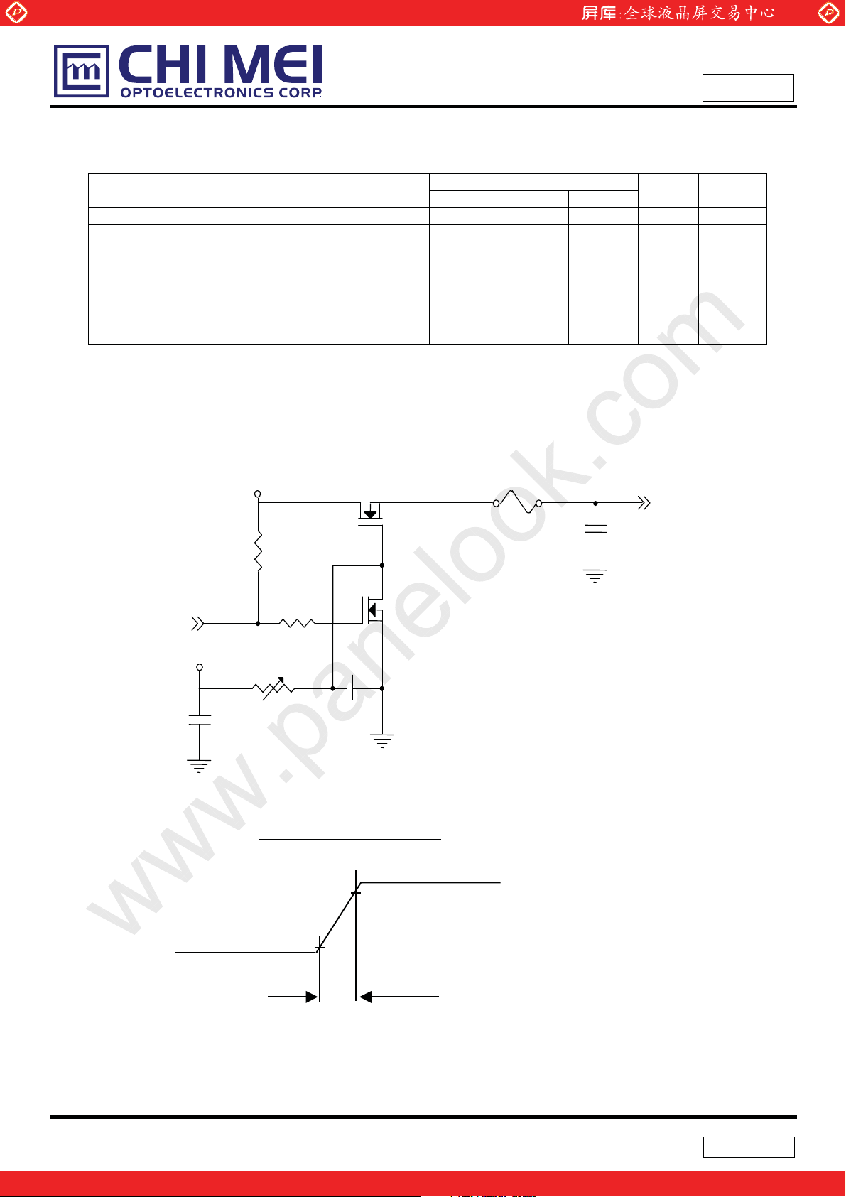
3.1 TFT LCD MODULE Ta = 25 ± 2 ºC
Parameter Symbol
Min. Typ. Max.
Power Supply Voltage Vcc (11.5) 12.0 (12.5) V Ripple Voltage VRP (0.1) mV Power Supply Current Icc - (600) (1,200) mA (1)
Rush Current I
(5.8) A (2)
RUSH
LVDS differential input voltage (High) Vih - - 100 mV
LVDS differential input voltage (Low) Vil -100 - - mV
LVDS common input voltage Vic TBD TBD TBD V
Logic “L” input voltage Vil Vss - TBD V
Note (1) Typical current situation: Color bar pattern, Vcc=12.0V, without rush current.
Maximum current situation: White Screen, Vcc=11.5V, without rush current.
Note (2) Measurement Conditions:
Value
Unit Note
Tentative
+5.0V
R1
47K
Q1 2SK1475
FUSE
C3
1uF
Vcc
(LCD Module Input)
(High to Low)
(Control Signal)
SW
+12V
C1
1uF
VR1
R2
1K
47K
0.01uF
Q2
2SK1470
C2
Vcc rising time is 0.2 ms
+12 V
0.9Vcc
0.1Vcc
GND
0.2 ms
6 / 21
The information described in this technical specification is tentative and it is possible to be changed without prior
notice. Please contact CMO ’s representative while your product design is based on this specification.
One step solution for LCD / PDP / OLED panel application: Datasheet, inventory and accessory!
Version 0.0
www.panelook.com
Page 7
Global LCD Panel Exchange Center
www.panelook.com
Issued Date: Dec. 26, 2002
Model No.: M201U3 - L01
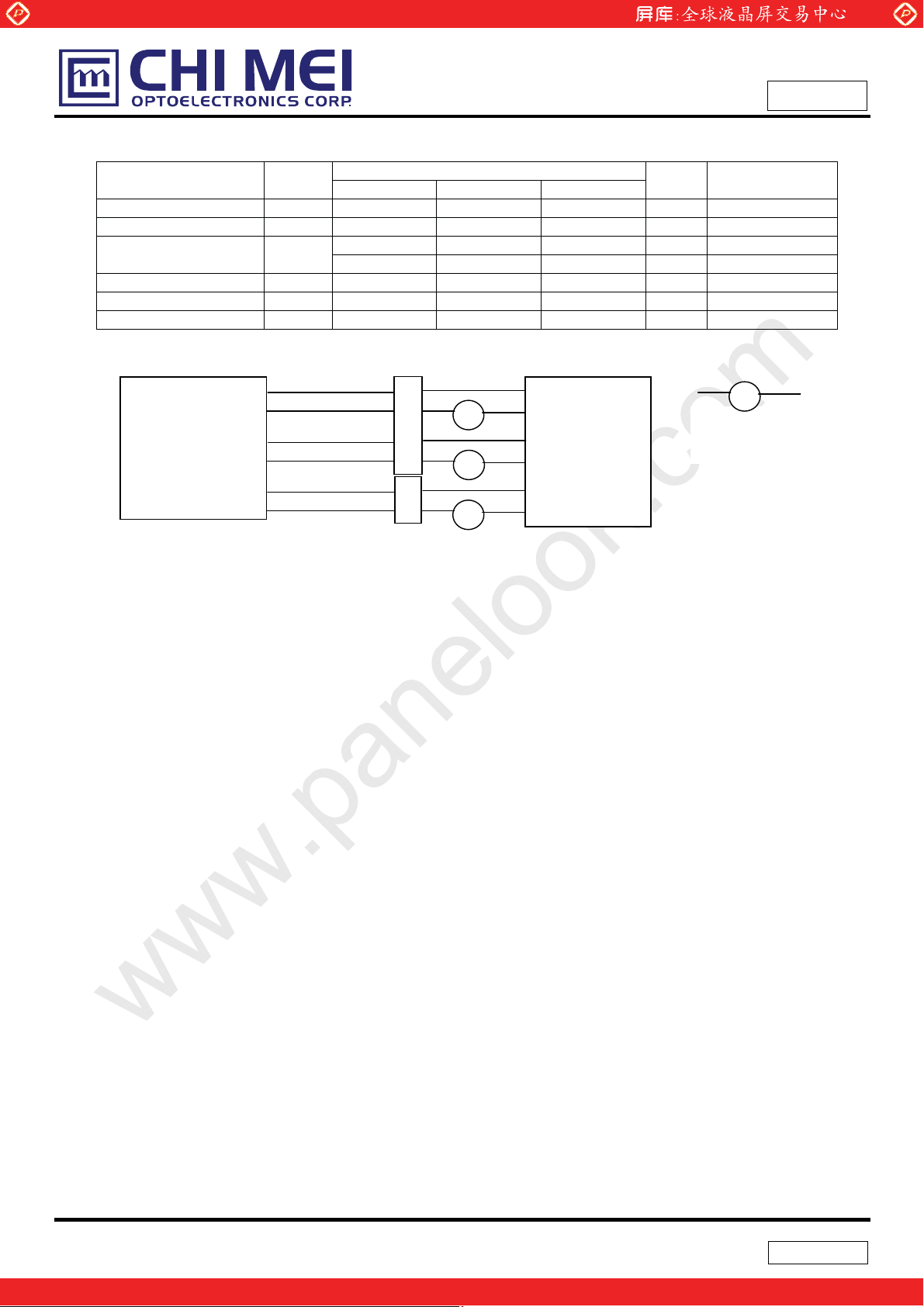
3.2 BACKLIGHT UNIT Ta = 25 ± 2 ºC
Parameter Symbol
Min. Typ. Max.
Lamp Input Voltage VL TBD (800) TBD V
Lamp Current IL (3.0) TBD (7.0) mA
Lamp Turn On Voltage VS
900 (25 oC) V
1,300 (0
Operating Frequency FL (40) (50) (60) KHz (3)
Lamp Life Time LBL 50,000 - - Hrs (5)
Power Consumption PL - (28.8) - W (4), IL = (6.0) mA
Note (1) Lamp current is measured by utilizing high frequency current meters as shown below:
Value
o
C) V
Unit Note
IL = (6.0) mA
RMS
(1)
RMS
(2)
RMS
(2)
RMS
Tentative
LCD
Module
HV (Pink)
LV (White)
HV (Blue)
LV (White)
HV (Pink)
LV (White)
1
1
2
2
3
1
4
2
5
A
Inverter
A
A
Current Meter
YOKOGAWA 2016
1
2
A
Note (2) The voltage shown above should be applied to the lamp for more than 1 second after startup.
Otherwise the lamp may not be turned on.
Note (3) The lamp frequency may produce interference with horizontal synchronous frequency from the
display, and this may cause line flow on the display. In order to avoid interference, the lamp
frequency should be detached from the horizontal synchronous frequency and its harmonics as far
as possible.
Note (4) P
= IL VL
L
Note (5) The lifetime of lamp can be defined as the time in which it continues to operate under the condition
Ta = 25 2
o
C and IL = (3.0) ~ (7.0) mArms until one of the following events occurs:
(a) When the brightness becomes or lower than 50% of its original value.
(b) When the effective ignition length becomes or lower than 80% of its original value. (Effective
ignition length is defined as an area that has less than 70% brightness compared to the
brightness in the center point.)
Note (6) The waveform of the voltage output of inverter must be area-symmetric and the design of the
inverter must have specifications for the modularized lamp. The performance of the Backlight,
such as lifetime or brightness, is greatly influenced by the characteristics of the DC-AC inverter for
the lamp. All the parameters of an inverter should be carefully designed to avoid producing too
much current leakage from high voltage output of the inverter. When designing or ordering the
inverter please make sure that a poor lighting caused by the mismatch of the Backlight and the
inverter (miss-lighting, flicker, etc.) never occurs. If the above situation is confirmed, the module
should be operated in the same manners when it is installed in your instrument.
7 / 21
The information described in this technical specification is tentative and it is possible to be changed without prior
notice. Please contact CMO ’s representative while your product design is based on this specification.
One step solution for LCD / PDP / OLED panel application: Datasheet, inventory and accessory!
Version 0.0
www.panelook.com
Page 8

Global LCD Panel Exchange Center
)
)
)
)
)
)
)
)
)
)
)
)
4. BLOCK DIAGRAM
4.1 TFT LCD MODULE
RXE0(+/-)
RXE1(+/-)
RXE2(+/-)
RXE3(+/-)
RXEC(+/-)
RXO0(+/-)
RXO1(+/-)
RXO2(+/-)
RXO3(+/-)
RXOC(+/-)
SELLVDS
Vcc
GND
INPUT CONNECTOR
(JAE / FI-X30S-HF)
VL
LAMP CONNECTOR
(JST / BHR-05VS-2,
(JST / BHR-05VS-2, BHSR-02VS-1)
LAMP CONNECTOR
www.panelook.com
LVDS RECEIVER /
TIMING CONTROLLER
DC/DC CONVERTER &
REFERENCE VOLTAGE
Issued Date: Dec. 26, 2002
Model No.: M201U3 - L01
Tentative
SCAN DRIVER IC
TFT LCD PANEL
(1600x3x1200)
DATA DRIVER IC
BACKLIGHT UNIT
4.2 BACKLIGHT UNIT
CN1
CN2 CN3
CN4
1 VH1 (TBD
4 VL1 (TBD
2 VH2 (TBD
5 VL2 (TBD
1 VH3 (TBD
2 VL3 (TBD
1 VH4 (TBD
2 VL4 (TBD
1 VH5 (TBD
4 VL5 (TBD
2 VH6 (TBD
5 VL6 (TBD
8 / 21
The information described in this technical specification is tentative and it is possible to be changed without prior
notice. Please contact CMO ’s representative while your product design is based on this specification.
One step solution for LCD / PDP / OLED panel application: Datasheet, inventory and accessory!
Version 0.0
www.panelook.com
Page 9

Global LCD Panel Exchange Center
5. INPUT TERMINAL PIN ASSIGNMENT
5.1 TFT LCD MODULE
Pin Name Description
1 VCC +12V power supply
2 VCC +12V power supply
3 VCC +12V power supply
4 TST Test Pin *3
5 PD LVDS Core Power Down
6 SELLVDS Select LVDS data order *4
7 GND Ground
8 RXE3+ Positive LVDS differential data input. Channel E3 (even)
9 RXE3- Negative LVDS differential data input. Channel E3 (even)
10 RXEC+ Positive LVDS differential clock input. (even)
11 RXEC- Negative LVDS differential clock input. (even)
12 RXE2+ Positive LVDS differential data input. Channel E2 (even)
13 RXE2- Negative LVDS differential data input. Channel E2 (even)
14 GND Ground
15 RXE1+ Positive LVDS differential data input. Channel E1 (even)
16 RXE1- Negative LVDS differential data input. Channel E1 (even)
17 GND Ground
18 RXE0+ Positive LVDS differential data input. Channel E0 (even)
19 RXE0- Negative LVDS differential data input. Channel E0 (even)
20 RXO3+ Positive LVDS differential data input. Channel O3 (odd)
21 RXO3- Negative LVDS differential data input. Channel O3(odd)
22 RXOC+ Positive LVDS differential clock input. (odd)
23 RXOC- Negative LVDS differential clock input. (odd)
24 GND Ground
25 RXO2+ Positive LVDS differential data input. Channel O2 (odd)
26 RXO2- Negative LVDS differential data input. Channel O2 (odd)
27 RXO1+ Positive LVDS differential data input. Channel O1 (odd)
28 RXO1- Negative LVDS differential data input. Channel O1 (odd)
29 RXO0+ Positive LVDS differential data input. Channel O0 (odd)
30 RXO0- Negative LVDS differential data input. Channel O0 (odd)
Note (1) Connector Part No.: FI-X30S-HF (JAE)
www.panelook.com
Issued Date: Dec. 26, 2002
Model No.: M201U3 - L01
Tentative
Note (2) Mating Connector Part No.: FI-X30M or FI-X30H or FI-X30C (JAE)
Note (3) Keep open. (Internal test use only)
Note (4) 3.3V CMOS signal input. (High or Low)
9 / 21
The information described in this technical specification is tentative and it is possible to be changed without prior
notice. Please contact CMO ’s representative while your product design is based on this specification.
Version 0.0
One step solution for LCD / PDP / OLED panel application: Datasheet, inventory and accessory!
www.panelook.com
Page 10

Global LCD Panel Exchange Center
5.2 LVDS DATA ASSIGNMENT
www.panelook.com
Issued Date: Dec. 26, 2002
Model No.: M201U3 - L01
Tentative
Note, RSVD(reserved) pin on a transmitter should be connected with Ground,
Input odd or even data depending on the display position of the LCD module.
10 / 21
The information described in this technical specification is tentative and it is possible to be changed without prior
notice. Please contact CMO ’s representative while your product design is based on this specification.
One step solution for LCD / PDP / OLED panel application: Datasheet, inventory and accessory!
Version 0.0
www.panelook.com
Page 11

Global LCD Panel Exchange Center
5.3 BACKLIGHT UNIT
NO. Pin No. Symbol Description Color
1 VH1 / VH5 High Voltage TBD
CN1 /
CN4 /
CN3 /
Note (1) Connector Part No.: CN1, 4 / BHR-05VS-2, CN2,3 / BHSR-02VS-1 (JST)
Note (2) Mating connector Part No.: CN1,4 / SM05(9.0)B-BHS-1-TB, CN2, 3 / SM02B-BHSS-1-TB (JST)
2 VH2 / VH6 High Voltage TBD
3 - NC
4 VL1 / VL5 Low Voltage TBD
5 VL2 / VL6 Low Voltage TBD
1 VH3 / VH4 High Voltage TBD CN2 /
2 VL3 / VL4 Low Voltage TBD
5.4 COLOR DATA INPUT ASSIGNMENT
The brightness of each primary color (red, green and blue) is based on the 8-bit gray scale data input for
www.panelook.com
Issued Date: Dec. 26, 2002
Model No.: M201U3 - L01
Tentative
the color. The higher the binary input, the brighter the color. The table below provides the assignment of
color versus data input.
Data Signal
Color
R7 R6 R5 R4 R3 R2 R1 R0 R7 R6 G5 G4 G3 G2 G1 G0 R7 R6 B5 B4 B3 B2 B1 B0
Black
Red
Green
Basic
Colors
Gray
Scale
Of
Red
Gray
Scale
Of
Green
Gray
Scale
Of
Blue
Note (1) 0: Low Level Voltage, 1: High Level Voltage
Blue
Cyan
Magenta
Ye ll ow
White
Red(0) / Dark
Red(1)
Red(2)
:
:
Red(253)
Red(254)
Red(255)
Green(0) / Dark
Green(1)
Green(2)
:
:
Green(253)
Green(254)
Green(255)
Blue(0) / Dark
Blue(1)
Blue(2)
:
:
Blue(253)
Blue(254)
Blue(255)
0
0
1
1
0
0
0
0
0
0
1
1
1
1
1
1
0
0
0
0
0
0
:
:
:
:
1
1
1
1
1
1
0
0
0
0
0
0
:
:
:
:
0
0
0
0
0
0
0
0
0
0
0
0
:
:
:
:
0
0
0
0
0
0
Red Green Blue
0
0
0
0
0
0
0
0
0
0
0
0
0
0
0
0
0
0
0
0
0
1
1
1
1
1
1
0
0
0
0
0
0
0
0
0
0
0
0
0
0
0
0
0
0
0
0
0
1
1
1
1
1
1
1
1
0
0
0
0
0
0
0
0
0
0
0
0
0
0
0
0
0
0
0
0
0
1
1
1
1
1
1
1
0
0
0
0
0
0
1
1
1
1
1
1
1
1
1
1
1
1
1
1
1
1
1
1
1
1
1
0
0
0
0
0
0
0
0
1
1
1
1
1
1
1
1
1
1
1
1
1
1
1
1
1
1
1
1
1
0
0
0
0
0
0
0
1
1
1
1
1
1
1
1
1
1
1
1
1
1
1
1
1
1
1
1
1
0
0
0
0
0
0
0
0
0
0
0
0
0
0
0
0
0
0
0
0
0
0
0
0
0
0
1
0
0
0
0
0
0
0
0
0
0
0
0
0
0
0
0
0
0
0
1
0
0
0
0
0
0
0
0
0
0
0
0
0
0
0
0
:
:
:
:
:
:
:
:
:
:
:
:
:
:
:
:
:
:
:
:
:
:
:
:
:
:
:
:
:
:
:
:
:
:
:
:
:
:
:
:
:
:
1
1
1
1
0
1
0
0
0
0
0
0
0
0
0
0
0
0
0
0
0
1
1
1
1
1
0
0
0
0
0
0
0
0
0
0
0
0
0
0
0
0
1
1
1
1
1
1
0
0
0
0
0
0
0
0
0
0
0
0
0
0
0
0
0
0
0
0
0
0
0
0
0
0
0
0
0
0
0
0
0
0
0
0
0
0
0
0
0
0
0
0
0
0
0
0
0
1
0
0
0
0
0
0
0
0
0
0
0
0
0
0
0
0
0
0
0
1
0
0
0
0
0
0
0
0
:
:
:
:
:
:
:
:
:
:
:
:
:
:
:
:
:
:
:
:
:
:
:
:
:
:
:
:
:
:
:
:
:
:
:
:
:
:
:
:
:
:
0
0
0
0
0
0
1
1
1
1
1
1
0
1
0
0
0
0
0
0
0
0
0
0
0
0
0
1
1
1
1
1
1
1
0
0
0
0
0
0
0
0
0
0
0
0
0
0
1
1
1
1
1
1
1
1
0
0
0
0
0
0
0
0
0
0
0
0
0
0
0
0
0
0
0
0
0
0
0
0
0
0
0
0
0
0
0
0
0
0
0
0
0
0
0
0
0
0
0
0
0
0
0
0
0
0
0
0
0
0
0
0
0
0
0
0
0
0
0
0
0
0
0
0
0
1
:
:
:
:
:
:
:
:
:
:
:
:
:
:
:
:
:
:
:
:
:
:
:
:
:
:
:
:
:
:
:
:
:
:
:
:
:
:
:
:
:
:
0
0
0
0
0
0
0
0
0
0
0
0
0
0
1
1
1
1
1
1
0
0
0
0
0
0
0
0
0
0
0
0
0
0
0
1
1
1
1
1
1
1
0
0
0
0
0
0
0
0
0
0
0
0
0
0
1
1
1
1
1
1
1
0
0
0
1
1
1
0
1
0
0
0
:
:
0
0
0
0
0
0
:
:
0
0
0
0
1
0
:
:
1
0
1
11 / 21
The information described in this technical specification is tentative and it is possible to be changed without prior
notice. Please contact CMO ’s representative while your product design is based on this specification.
One step solution for LCD / PDP / OLED panel application: Datasheet, inventory and accessory!
Version 0.0
www.panelook.com
Page 12

Global LCD Panel Exchange Center
6. INTERFACE TIMING
6.1 INPUT SIGNAL TIMING SPECIFICATIONS
The input signal timing specifications are shown as the following table and timing diagram.
Signal Item Symbol Min. Typ. Max. Unit Note
Period Tc 11.765 12.345 20.000 ns
Frequency 1/Tc 60 81 85 MHZ
DCLK signal (Clock)
DCLK-Data Timing
ENAB signal
Note (1) Horizontal display position is specified by the rise of ENAB. The data latched at falling edge of
Duty Tch/Tc 45 50 55 %
High time TclkH 3.5 - - ns
Low time TclkL 3.5 - - ns
Setup time Tset 3 - - ns
Hold time Thold 2 - - ns
Horizontal period Th 865 1080 1130 DCLK *1
Hor. Period Th 13.0 13.3 14.65 us
Hor. Display period Thd 800 800 800 DLCK *2
Vertical period Tv 1207 1250 1280 Hz
Ver. Frequency 1/Tv (50) 60 (62) Hz
Ver. Display period Tvd 1200 1200 1200 Hz
Data-ENAB timing Tdn - 0 - DCLK *3
www.panelook.com
Issued Date: Dec. 26, 2002
Model No.: M201U3 - L01
Tentative
DCLK after rise of ENAB is displayed at the left edge of the display area.
Vertical display position is specified by the rise of ENAB after low level continuation over 5500
DCLK. The data latched at the rise of ENAB is displayed at the top line of the display area.
Note (2) If the “High” level of ENAB is less than 800 DCLK, black color is displayed at the rest of display
area.
Note (3) If ENAB does not synchronize with the effective display data, the display position does not fit to
the display area.
Note (4) Because of this module is operated by DE only mode, Hsync and Vsync input signals should be
set to low logic level or ground. Otherwise, this module would operate abnormally.
12 / 21
The information described in this technical specification is tentative and it is possible to be changed without prior
notice. Please contact CMO ’s representative while your product design is based on this specification.
One step solution for LCD / PDP / OLED panel application: Datasheet, inventory and accessory!
Version 0.0
www.panelook.com
Page 13

Global LCD Panel Exchange Center
www.panelook.com
Issued Date: Dec. 26, 2002
Model No.: M201U3 - L01
Tentative
INPUT SIGNAL TIMING DIAGRAM
13 / 21
The information described in this technical specification is tentative and it is possible to be changed without prior
notice. Please contact CMO ’s representative while your product design is based on this specification.
Version 0.0
One step solution for LCD / PDP / OLED panel application: Datasheet, inventory and accessory!
www.panelook.com
Page 14

Global LCD Panel Exchange Center
6.2 POWER ON/OFF SEQUENCE
The sequence of input signals and On/Off of the power supply of the LCD module should be in the
specification shown as below to prevent latch-up of the driver ICs and DC driving of LCD panel.
www.panelook.com
Issued Date: Dec. 26, 2002
Model No.: M201U3 - L01
Tentative
Power Supply Sequence (Logic)
14 / 21
The information described in this technical specification is tentative and it is possible to be changed without prior
notice. Please contact CMO ’s representative while your product design is based on this specification.
One step solution for LCD / PDP / OLED panel application: Datasheet, inventory and accessory!
Version 0.0
www.panelook.com
Page 15

Global LCD Panel Exchange Center
7. OPTICAL CHARACTERISTICS
7.1 TEST CONDITIONS
Item Symbol Value Unit
Ambient Temperature Ta
Ambient Humidity Ha
Supply Voltage VCC 5.0 V
Input Signal According to typical value in "3. ELECTRICAL CHARACTERISTICS"
Inverter Current IL 6.0 mA
Inverter Driving Frequency FL 50 KHz
Inverter --
7.2 OPTICAL SPECIFICATIONS
The relative measurement methods of optical characteristics are shown in 7.2. The following items should
be measured under the test conditions described in 7.1 and stable environment shown in Note (6).
Item Symbol Condition Min. Typ. Max. Unit Note
Contrast Ratio CR (400) (600) - - (2), (6)
Response Time
Center Luminance of White L
Average Luminance of White L
White Variation
Cross Talk CT - - TBD % (5), (6)
Red
Color
Chromaticity
Viewing Angle
Green
Blue
White
Horizontal
Ver t i c al
www.panelook.com
Issued Date: Dec. 26, 2002
Model No.: M201U3 - L01
Tentative
o
25r2
50r10
TR - (15) (30) ms
- (10) (25) ms
T
F
C
TBD (220) - cd/m2(4), (6)
AVE
GW
T
=0q, TY =0q
x
Rx TBD Ry TBD -
Viewing Normal Angle
(200) (250) - cd/m2(4), (6)
- TBD (1.40) - (6), (7)
Gx TBD Gy TBD Bx TBD -
By TBD Wx (0.283) (0.313) (0.343) Wy
Tx+
T
x
TY+
T
Y
CRt10
-
(0.299) (0.329) (0.359) -
(85) - (85) - (85) - (85) - -
C
%RH
(3)
(1), (6)
Deg.
15 / 21
The information described in this technical specification is tentative and it is possible to be changed without prior
notice. Please contact CMO ’s representative while your product design is based on this specification.
One step solution for LCD / PDP / OLED panel application: Datasheet, inventory and accessory!
Version 0.0
www.panelook.com
Page 16

Global LCD Panel Exchange Center
T
Note (1) Definition of Viewing Angle (Tx, Ty):
www.panelook.com
Issued Date: Dec. 26, 2002
Model No.: M201U3 - L01
Tentative
TX- = 90º
x-
6 o’clock
T
y- = 90º
y-
Note (2) Definition of Contrast Ratio (CR):
The contrast ratio can be calculated by the following expression.
Normal
Tx = Ty = 0º
Ty- Ty
Tx
Tx
y+
12 o’clock direction
T
y+ = 90º
x+
TX+ = 90º
Contrast Ratio (CR) = L255 / L0
L255: Luminance of gray level 255
L 0: Luminance of gray level 0
CR = CR (5)
CR (X) is corresponding to the Contrast Ratio of the point X at Figure in Note (7).
Note (3) Definition of Response Time (T
100%
90%
Optical
Response
Gray Level 255
10%
0%
, TF):
R
Gray Level 0
Gray Level 255
T
F
T
R
ime
16 / 21
The information described in this technical specification is tentative and it is possible to be changed without prior
notice. Please contact CMO ’s representative while your product design is based on this specification.
One step solution for LCD / PDP / OLED panel application: Datasheet, inventory and accessory!
Version 0.0
www.panelook.com
Page 17

Global LCD Panel Exchange Center
A
(
)
A
(
)
(
)
www.panelook.com
Issued Date: Dec. 26, 2002
Model No.: M201U3 - L01
Tentative
Note (4) Definition of Luminance of White (LC, L
Measure the luminance of gray level 255 at center point and 5 points
LC = L (5)
L
= [L (1)+ L (2)+ L (3)+ L (4)+ L (5)] / 5
AVE
L (x) is corresponding to the luminance of the point X at Figure in Note (7).
Note (5) Definition of Cross Talk (CT):
CT = | Y
– YA | / YA u 100 (%)
B
Where:
Y
= Luminance of measured location without gray level 0 pattern (cd/m2)
A
Y
= Luminance of measured location with gray level 0 pattern (cd/m2)
B
(0, 0)
ctive Area
Y
(D/8,W/2)
A, L
Gray 128
Y
(D/2,7W/8)
A, D
Y
Y
D,W
A, U
A, R
):
AVE
(D/2,W/8)
(7D/8,W/2)
(D/4,W/4)
Y
(D/8,W/2)
B, L
Y
(D/2,7W/8)
B, D
0, 0
ctive Area
Gray 0
Gray 128
Y
(D/2,W/8)
B, U
Y
(7D/8,W/2)
B, R
(3D/4,3W/4)
D,W
Note (6) Measurement Setup:
The LCD module should be stabilized at given temperature for 20 minutes to avoid abrupt
temperature change during measuring. In order to stabilize the luminance, the measurement
should be executed after lighting Backlight for 20 minutes in a windless room.
LCD Module
LCD Panel
Center of the Screen
500 mm
Photometer
(TOPCON BM-5A)
Field of View = 2º
Light Shield Room
(Ambient Luminance < 2 lux)
17 / 21
The information described in this technical specification is tentative and it is possible to be changed without prior
notice. Please contact CMO ’s representative while your product design is based on this specification.
One step solution for LCD / PDP / OLED panel application: Datasheet, inventory and accessory!
Version 0.0
www.panelook.com
Page 18

Global LCD Panel Exchange Center
Note (7) Definition of White Variation (GW):
Measure the luminance of gray level 255 at 5 points
GW = Maximum [L (1), L (2), L (3), L (4), L (5)] / Minimum [L (1), L (2), L (3), L (4), L (5)]
www.panelook.com
Issued Date: Dec. 26, 2002
Model No.: M201U3 - L01
Tentative
W
W/10
W/2
W/10
Vertical Line
D/10 D/2
1 2
3
Horizontal Line
D
5
Active Area
D/10
4
X
: Test Point
X=1 to 5
18 / 21
The information described in this technical specification is tentative and it is possible to be changed without prior
notice. Please contact CMO ’s representative while your product design is based on this specification.
Version 0.0
One step solution for LCD / PDP / OLED panel application: Datasheet, inventory and accessory!
www.panelook.com
Page 19

Global LCD Panel Exchange Center
www.panelook.com
Issued Date: Dec. 26, 2002
Model No.: M201U3 - L01
Tentative
8. PRECAUTIONS
8.1 ASSEMBLY AND HANDLING PRECAUTIONS
(1) Do not apply rough force such as bending or twisting to the module during assembly.
(2) To assemble or install module into user’s system can be only in clean working areas. The dust and oil
may cause electrical short or worsen the polarizer.
(3) It’s not permitted to have pressure or impulse on the module because the LCD panel and Backlight will
be damaged.
(4) Always follow the correct power sequence when LCD module is connecting and operating. This can
prevent damage to the CMOS LSI chips during latch-up.
(5) Do not pull the I/F connector in or out while the module is operating.
(6) Do not disassemble the module.
(7) Use a soft dry cloth without chemicals for cleaning, because the surface of polarizer is very soft and
easily scratched.
(8) It is dangerous that moisture come into or contacted the LCD module, because moisture may damage
LCD module when it is operating.
(9) High temperature or humidity may reduce the performance of module. Please store LCD module within
the specified storage conditions.
(10) When ambient temperature is lower than 10ºC may reduce the display quality. For example, the
response time will become slowly, and the starting voltage of CCFL will be higher than room
temperature.
8.2 SAFETY PRECAUTIONS
(1) The startup voltage of Backlight is approximately 1000 Volts. It may cause electrical shock while
assembling with inverter. Do not disassemble the module or insert anything into the Backlight unit.
(2) If the liquid crystal material leaks from the panel, it should be kept away from the eyes or mouth. In
case of contact with hands, skin or clothes, it has to be washed away thoroughly with soap.
(3) After the module’s end of life, it is not harmful in case of normal operation and storage.
19 / 21
The information described in this technical specification is tentative and it is possible to be changed without prior
notice. Please contact CMO ’s representative while your product design is based on this specification.
One step solution for LCD / PDP / OLED panel application: Datasheet, inventory and accessory!
Version 0.0
www.panelook.com
Page 20

Global LCD Panel Exchange Center
www.panelook.com
Issued Date: Dec. 26, 2002
Model No.: M201U3 - L01
Tentative
M201U3- L01
20 / 21
The information described in this technical specification is tentative and it is possible to be changed without prior
notice. Please contact CMO ’s representative while your product design is based on this specification.
One step solution for LCD / PDP / OLED panel application: Datasheet, inventory and accessory!
Version 0.0
www.panelook.com
Page 21

Global LCD Panel Exchange Center
www.panelook.com
Issued Date: Dec. 26, 2002
Model No.: M201U3 - L01
Tentative
M201U3- L01
21 / 21
The information described in this technical specification is tentative and it is possible to be changed without prior
notice. Please contact CMO ’s representative while your product design is based on this specification.
One step solution for LCD / PDP / OLED panel application: Datasheet, inventory and accessory!
Version 0.0
www.panelook.com
 Loading...