

Page 1
Global LCD Panel Exchange Center
www.panelook.com
One step solution for LCD / PDP / OLED panel application: Datasheet, inventory and accessory!
www.panelook.com
Page 2
Global LCD Panel Exchange Center
Version Date
Ver 1.0 Feb.27,’02 All
Page
(New)
Section Description
www.panelook.com
REVISION HISTORY
All Tentative Specification was first issued.
Issued Date: Feb. 27, 2002
Model No.: M190E1 -L01
Tentative
2 / 31
The information described in this technical specification is tentative and it is possible to be changed without prior
notice. Please contact CMO ’s representative while your product design is based on this specification.
One step solution for LCD / PDP / OLED panel application: Datasheet, inventory and accessory!
Version 0.0
www.panelook.com
Page 3
Global LCD Panel Exchange Center
www.panelook.com
Issued Date: Feb. 27, 2002
Model No.: M190E1 -L01
- TABLE OF CONTENTS -
1. APPLICATIONS
2. PRODUCT NAME AND MODEL NUMBER
2-1 Product Name •••••••••••••••••••••••••••••••••••••••••••••••••••••••••••••••••••••••••••••••••••••••••••••••••••••••••••4
•••••••••••••••••••••••••••••••••••••••••••••••••••••••••••••••••••••••••••••••••••••••••••••••••••••••••••4
•••••••••••••••••••••••••••••••••••••••••••••••••••••••••••••••••••••••4
Tentative
2-2 Model Number •••••••••••••••••••••••••••••••••••••••••••••••••••••••••••••••••••••••••••••••••••••••••••••••••••••••••••
4
3. OVERVIEW •••••••••••••••••••••••••••••••••••••••••••••••••••••••••••••••••••••••••••••••••••••••••••••••••••••••••••••••••4
4. CONFIGURATION
5. MECHANICAL SPECIFICATIONS
6. ABSOLUTE MAXIMUM RATINGS
7. RECOMMENDED OPERATION RATING
8. ELECTRICAL SPECIFICATIONS
9. OPTICAL SPECIFICATIONS
10. INTERFACE SPECIFICATIONS
10-1 Signal Decriptions •••••••••••••••••••••••••••••••••••••••••••••••••••••••••••••••••••••••••••••••••••••••••••••••••••11
10-2 LVDS Data Assignment •••••••••••••••••••••••••••••••••••••••••••••••••••••••••••••••••••••••••••••••••••••••••••••
10-3 Color Data Assignment •••••••••••••••••••••••••••••••••••••••••••••••••••••••••••••••••••••••••••••••••••••••••••••
10-4 Input Signal Timing ••••••••••••••••••••••••••••••••••••••••••••••••••••••••••••••••••••••••••••••••••••••••••••••••••
10-5 Correspondence between Data and Display Position ••••••••••••••••••••••••••••••••••••••••••••••••••••••••
10-6 Power Supply Sequence •••••••••••••••••••••••••••••••••••••••••••••••••••••••••••••••••••••••••••••••••••••••••••
••••••••••••••••••••••••••••••••••••••••••••••••••••••••••••••••••••••••••••••••••••••••••••••••••••••••4
•••••••••••••••••••••••••••••••••••••••••••••••••••••••••••••••••••••••••••••••••••5
•••••••••••••••••••••••••••••••••••••••••••••••••••••••••••••••••••••••••••••••••••5
•••••••••••••••••••••••••••••••••••••••••••••••••••••••••••••••••••••••••5
••••••••••••••••••••••••••••••••••••••••••••••••••••••••••••••••••••••••••••••••••••6
••••••••••••••••••••••••••••••••••••••••••••••••••••••••••••••••••••••••••••••••••••••••••7
•••••••••••••••••••••••••••••••••••••••••••••••••••••••••••••••••••••••••••••••••••11
12
13
14
16
16
11. BACK-LIGHT SPECIFICATIONS •••••••••••••••••••••••••••••••••••••••••••••••••••••••••••••••••••••••••••••••••••17
11-1 Pin Configuration for Back-light ••••••••••••••••••••••••••••••••••••••••••••••••••••••••••••••••••••••••••••••••••••17
11-2 CCFL ••••••••••••••••••••••••••••••••••••••••••••••••••••••••••••••••••••••••••••••••••••••••••••••••••••••••••••••••••••
17
11-3 Life •••••••••••••••••••••••••••••••••••••••••••••••••••••••••••••••••••••••••••••••••••••••••••••••••••••••••••••••••••••••
12. APPEARANCE SPECIFICATIONS
12-1 Appearance ••••••••••••••••••••••••••••••••••••••••••••••••••••••••••••••••••••••••••••••••••••••••••••••••••••••••••••18
12-2 Dot Defect ••••••••••••••••••••••••••••••••••••••••••••••••••••••••••••••••••••••••••••••••••••••••••••••••••••••••••••••
•••••••••••••••••••••••••••••••••••••••••••••••••••••••••••••••••••••••••••••••••18
17
19
13. ENVIRONMENTAL SPECIFICATIONS ••••••••••••••••••••••••••••••••••••••••••••••••••••••••••••••••••••••••••••20
14. INDICATIONS
15. PACKAGING
15-1 Packing Specifications ••••••••••••••••••••••••••••••••••••••••••••••••••••••••••••••••••••••••••••••••••••••••••••••••22
15-2 Packing Method ••••••••••••••••••••••••••••••••••••••••••••••••••••••••••••••••••••••••••••••••••••••••••••••••••••••••
••••••••••••••••••••••••••••••••••••••••••••••••••••••••••••••••••••••••••••••••••••••••••••••••••••••••••••••21
••••••••••••••••••••••••••••••••••••••••••••••••••••••••••••••••••••••••••••••••••••••••••••••••••••••••••••••••22
22
16. WARRANTY •••••••••••••••••••••••••••••••••••••••••••••••••••••••••••••••••••••••••••••••••••••••••••••••••••••••••••••••••26
17.PRECAUTIONS
18. PRECAUTIONS FOR USE
19. MISCELLANEOUS
20. MECHANICAL DRAWINGS
The information described in this technical specification is tentative and it is possible to be changed without prior
notice. Please contact CMO ’s representative while your product design is based on this specification.
•••••••••••••••••••••••••••••••••••••••••••••••••••••••••••••••••••••••••••••••••••••••••••••••••••••••••••••26
•••••••••••••••••••••••••••••••••••••••••••••••••••••••••••••••••••••••••••••••••••••••••••••31
••••••••••••••••••••••••••••••••••••••••••••••••••••••••••••••••••••••••••••••••••••••••••••••••••••••••31
••••••••••••••••••••••••••••••••••••••••••••••••••••••••••••••••••••••••••••••••••••••••••••32
3 / 31
Version 0.0
One step solution for LCD / PDP / OLED panel application: Datasheet, inventory and accessory!
www.panelook.com
Page 4
Global LCD Panel Exchange Center
1. APPLICATION
This specification is applied to the 19-inch SXGA supported TFT-LCD module.
2. PRODUCT NAME AND MODEL NUMBER
2.1 Product Name: LCD Module
2.2 Model Name: M190E1 -L01
3. OVERVIEW
This LCD module has a TFT active matrix type liquid crystal panel 1280x1024 pixels, and diagonal size
of 48cm(19-inch). This LCD has a LVDS dual interface and can display 16,777,216 colors.
www.panelook.com
Issued Date: Feb. 27, 2002
Model No.: M190E1 -L01
Tentative
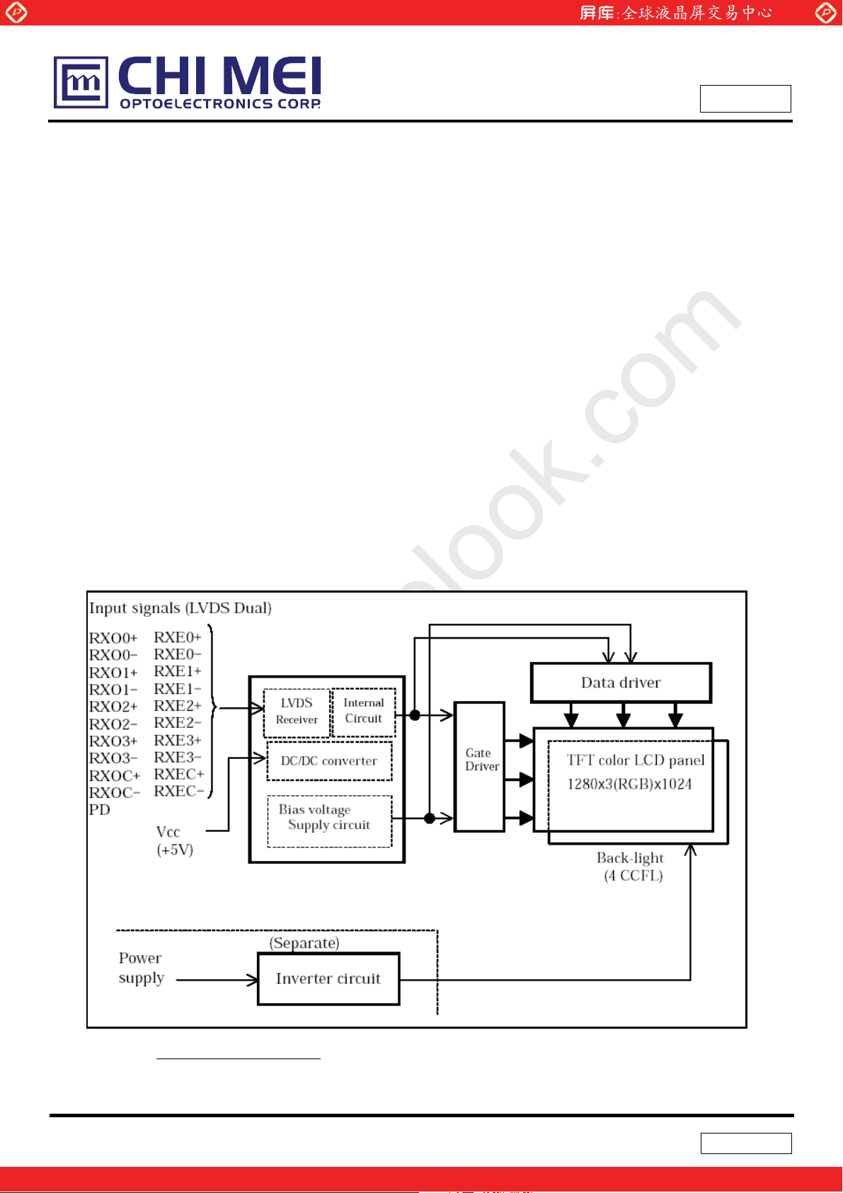
4. CONFIGURATION
This LCD module consists of a color TFT-LCD panel that is mounted with TFT driver ICs, a cold-cathode
fluorescent tube back-light. The inverter for the back-light is not included.
Figure 4-1 shows a block disgram of this LCD module.
Figure 4-1 Block Diagram.
The information described in this technical specification is tentative and it is possible to be changed without prior
notice. Please contact CMO ’s representative while your product design is based on this specification.
One step solution for LCD / PDP / OLED panel application: Datasheet, inventory and accessory!
4 / 31
Version 0.0
www.panelook.com
Page 5

Global LCD Panel Exchange Center
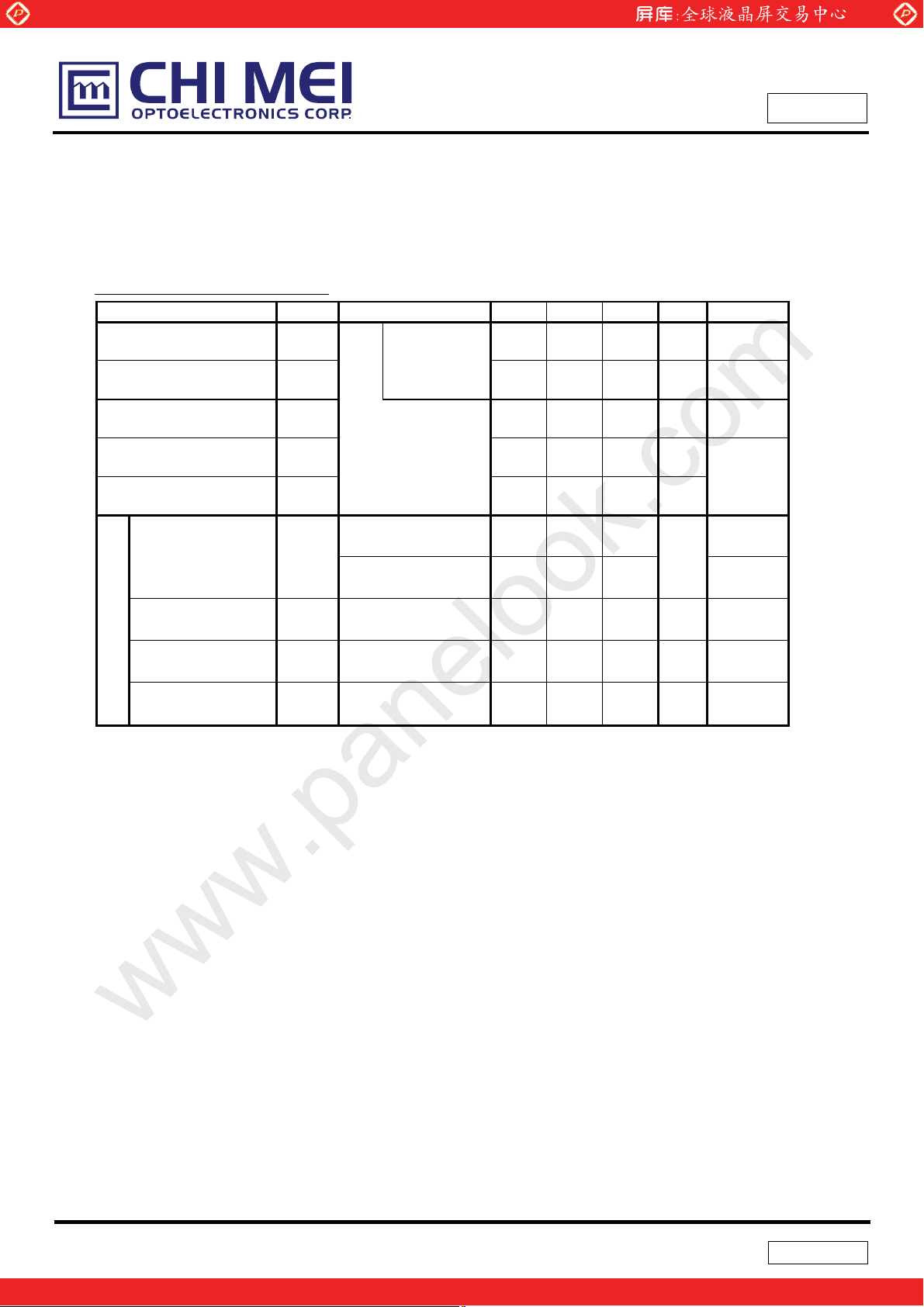
5. MECHANICAL SPECIFICATIONS
Table 5-1 shows the mechanical specifications of this LCD module.
www.panelook.com
Issued Date: Feb. 27, 2002
Model No.: M190E1 -L01
Tentative
Table 5-1 Mechanical Specifications.
Item Specification Unit Remark
Dimensions 414x335x23(TYP.) mm
Display Resolution (1280x3)x1024 --
Display Dot Area 376.32x301.056 mm
Dot Pitch (0.098x3)x0.294 mm
Aspect Ratio 5:4 --
Weight 3,000 MAX g
FG-SG Short Circuit --
Edge type back-light is used.
(I 2.6 CCFLx4)
Without inverter.
For details on dimensions,
See dimensional outline drawing.
(at page 32, 33, 34: Figure 19-1, 2, 3)
Excluding inverter.
6. ABSOLUTE MAXIMUM RATING
Table 6-1 shows the absolute maximum rating of this LCD module.
Table 6-1 Absolute Maximum Rating.
Item Symbol Condition MIN. TYP. MAX. Unit
Supplier Voltage VCC
Input Signal Voltage
(LVDS signal, PD)
IN
V
Ta=2 5
Ta=2 5
к
к
-0.3 -- 6.0 V
-0.3 -- 3.6 V
7. RECOMMENDED OPERATING CONDITIONS
Table 7-1 shows the recommended operating conditions of this LCD module.
Table 7-1 shows the Recommended Operating Conditions.
Item Symbol MIN. TYP. MAX. Unit
Supplier Voltage (Logic) VCC 4.75 -- 5.25 V
Ripple Voltage VCC VRP -- -- 0.1 V
5 / 31
The information described in this technical specification is tentative and it is possible to be changed without prior
notice. Please contact CMO ’s representative while your product design is based on this specification.
One step solution for LCD / PDP / OLED panel application: Datasheet, inventory and accessory!
Version 0.0
www.panelook.com
Page 6
Global LCD Panel Exchange Center
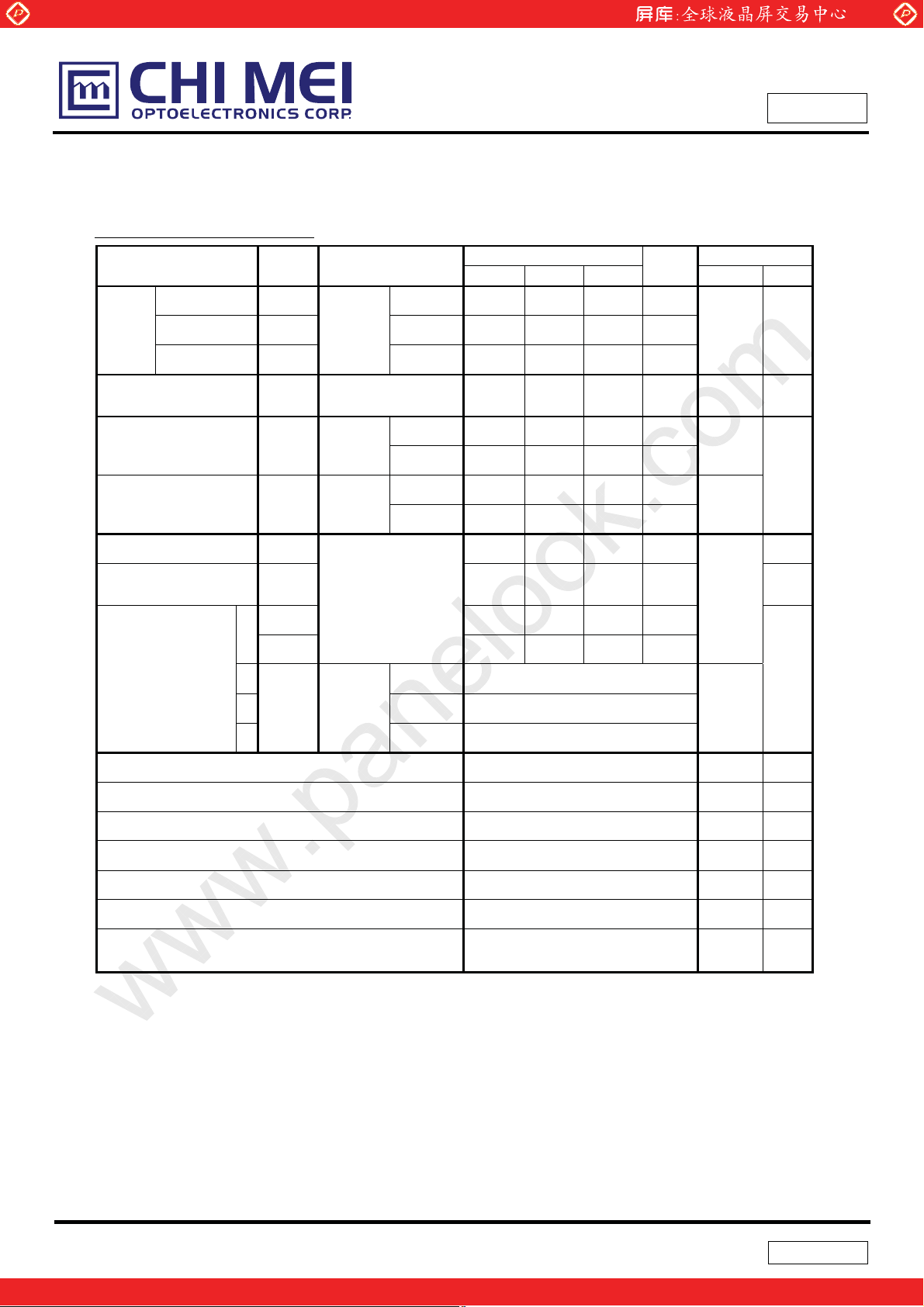
8. ELECTRICAL SPECIFICATIONS
Table 8-1 shows the electrical specifications of this LCD module. Figure 8-1 shows the measurement circuit.
Figure 8-2(A) shows the equivalent circuit of the logic signal input area. Figure 8-2(B) shows the equivalent
circuit of the supply voltage input area.
www.panelook.com
Issued Date: Feb. 27, 2002
Model No.: M190E1 -L01
Tentative
Table 8-1 Electrical Specifications.
Item Symbol Condition MIN. TYP. MAX. Unit Remark
Differential-input
Voltage (High)
Differential-input
Voltage (Low)
Supply Current
Supply Rush Current
Supply Rush Current
Duration(1.5A excess)
B
A
CCFL Turn on
C
Voltage
K
IH -- -- 100 mV
V
CM=+1.2V
V
V
I
SCC
I
SCC
T
V
IL
CC
CC=+5.0²0.25V
V
VSS=0V
CLK=54MHz
D
Ta=2 5к
fL=50kHz, Ta=25к
S
f
L=50kHz, Ta=0к
-100 -- -- mV
-- 800 1,500 mA *1
-- -- 3.5 A
-- -- 1 ms
-- 1,400 1,600
Vrms
-- -- 1,600
L=50kHz, Ta=0к
L
Lighting Voltage VL
I
G
Lighting Frequency fL VL=750Vrms 40 50 60 KHz
H
T
Tube Current
(*3)
f
I
L=7mA
L=50kHz
f
L
I
L=750Vrms
V
-- 750 -- Vrms
4 7 8
mArms
*2
*4
(*1) Typical current situation: Color bar pattern. V
Maximum current situation: White pattern. V
CC=5.0V
CC=4.75V
Without rush current.
(*2) These items prescribe the rush current of starting internal DC/DC.
Changing current to capacitors of V
CC is not prescribed.
(*3) Back-light specifications are valid when using a suitable inverter such as the FLCV-13.
(*4) Tube current (I
L) shows the value if the current that is consumed at one lamp.
This LCD module has 4 lamps. Each 2 lamps are placed at upper side and lower side of the display.
2 lamps are connected in parallel. Each low voltage terminals are connected with separate cables to
Back-light connectors.
6 / 31
The information described in this technical specification is tentative and it is possible to be changed without prior
notice. Please contact CMO ’s representative while your product design is based on this specification.
Version 0.0
One step solution for LCD / PDP / OLED panel application: Datasheet, inventory and accessory!
www.panelook.com
Page 7
Global LCD Panel Exchange Center
9. OPTICAL SPECIFICATIONS
Table 9-1 shows the optical specifications of this LCD module.
www.panelook.com
Issued Date: Feb. 27, 2002
Model No.: M190E1 -L01
Tentative
Table 9-1 Optical Specifications.
Item Symbol Condition
Horizontal
Visual
Angle
Contrast Ratio CR
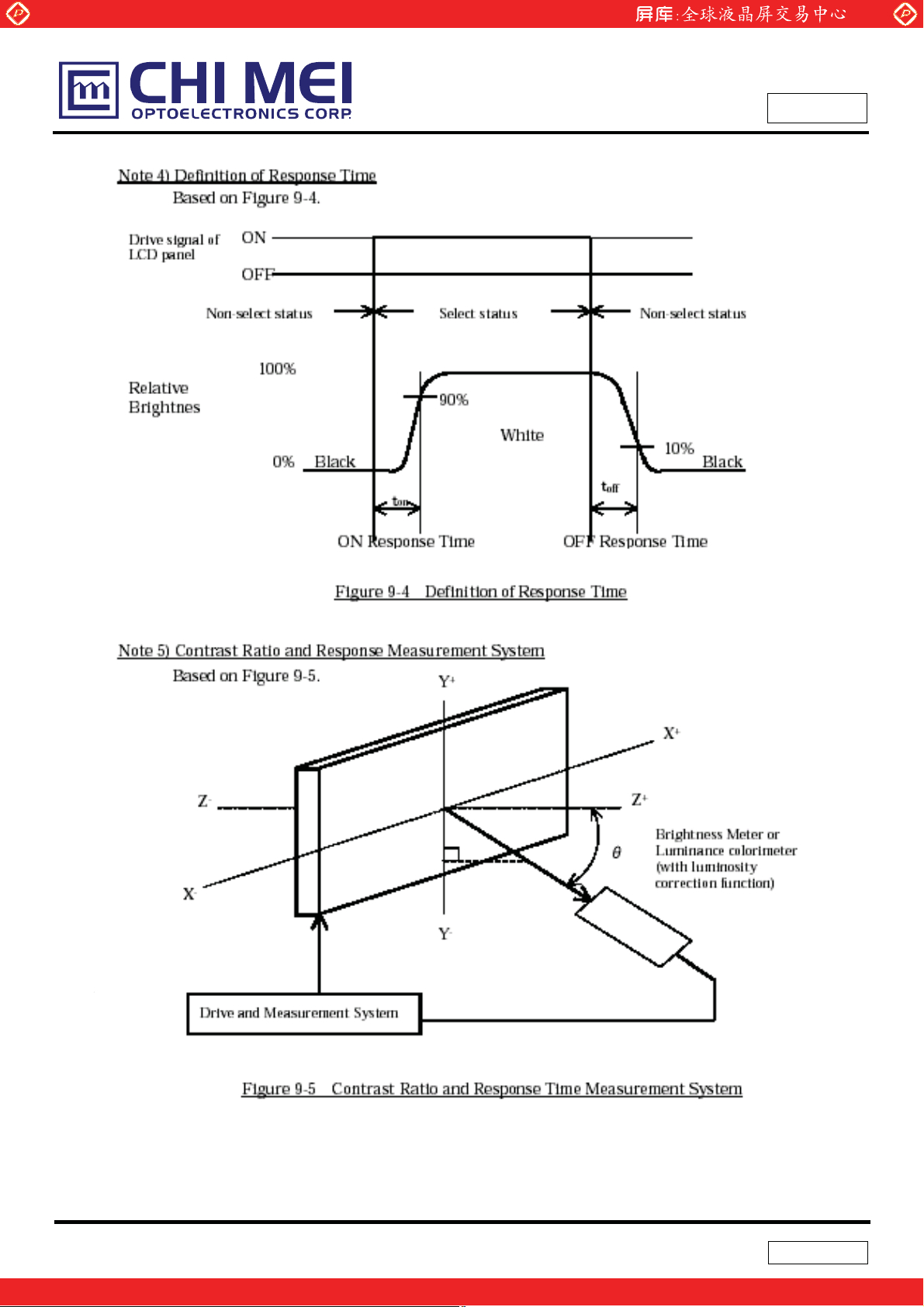
Response Time (ON)
(BW)
Response Time (OFF)
(WB)
Brightness
Brightness Uniformity
Chromaticity
Vertic al
All Direction
T
L, R
T
U, D
T
on
t
off
T
I
'I
x 0.283 0.313 0.343 --
W
y
R Red (0.648, 0.346) Typ.
(x, y)
G Green (0.292, 0.602) Typ.
Ta=25к
CR10
T
L, R, U, D =0°
T
L, R, U, D
=0°
T
L, R, U, D
=0°
T
L, R, U, D =0°
CC=5V
V
IL=7mA
Specifications Remark
MIN. TYP. MAX.
T
L, R=0°
T
U, D=0°
80 -- -- deg
Ta=2 5к
Ta=0 к
Ta=2 5к
Ta=0 к
85 -- -- deg
85 -- -- deg
350 500 -- --
-- 15 30 ms
-- 50 100 ms
10 25 ms
50 100 ms
200 250 -- cd/m2 (1)(5)
70 -- -- %
0.299 0.329 0.359 --
Unit
Note
White/
Black
White
*1
(1)(2)
(3)(5)
(6)
(1)(2)
(3)(5)
(1)
(4)
(5)
(1)(5)
(7)
(1)
(5)
B
LCD Panel Type TFT Color
Display Mode Normal Black
Wide Viewing Angle Technology MVA
Optimum Viewing Angle -- (symmetry) (6)
Display Color 16,777,216 (8-bit color)
Color of non-display area Black
Surface Treatment
(*1) Value at 15~20 minutes after lighting on.
(Note) •CS-1000 (MINOLTA Co., Ltd), BM-5A(Topcon) and the like should be used as a luminance colorimeter.
Field=1°, L=500mm.
•Back-light current = 7mA, Dark room condition (1 lux or less).
The information described in this technical specification is tentative and it is possible to be changed without prior
notice. Please contact CMO ’s representative while your product design is based on this specification.
Blue (0.150, 0.130) Typ.
Anti-glare
(Haze value: 25%, 2H)
7 / 31
Version 0.0
One step solution for LCD / PDP / OLED panel application: Datasheet, inventory and accessory!
www.panelook.com
Page 8
Global LCD Panel Exchange Center
www.panelook.com
Issued Date: Feb. 27, 2002
Model No.: M190E1 -L01
Tentative
8 / 31
The information described in this technical specification is tentative and it is possible to be changed without prior
notice. Please contact CMO ’s representative while your product design is based on this specification.
One step solution for LCD / PDP / OLED panel application: Datasheet, inventory and accessory!
Version 0.0
www.panelook.com
Page 9
Global LCD Panel Exchange Center
www.panelook.com
Issued Date: Feb. 27, 2002
Model No.: M190E1 -L01
Tentative
9 / 31
The information described in this technical specification is tentative and it is possible to be changed without prior
notice. Please contact CMO ’s representative while your product design is based on this specification.
One step solution for LCD / PDP / OLED panel application: Datasheet, inventory and accessory!
Version 0.0
www.panelook.com
Page 10
Global LCD Panel Exchange Center
www.panelook.com
Issued Date: Feb. 27, 2002
Model No.: M190E1 -L01
Tentative
10 / 31
The information described in this technical specification is tentative and it is possible to be changed without prior
notice. Please contact CMO ’s representative while your product design is based on this specification.
One step solution for LCD / PDP / OLED panel application: Datasheet, inventory and accessory!
Version 0.0
www.panelook.com
Page 11
Global LCD Panel Exchange Center
10. INTERFACE SPECIFICATIONS
10-1 Signal descriptions.
Table 10-1 shows the description and configuration of interface signal (CN1).
www.panelook.com
Issued Date: Feb. 27, 2002
Model No.: M190E1 -L01
Tentative
Table 10-1 Interface signals (CN1)
Pin Name I/O Description
1 RXO0- I Negative differential input
2 RXO0+ I Positive differential input
3 RXO1- I Negative differential input
4 RXO1+ I Positive differential input
5 RXO2- I Negative differential input
6 RXO2+ I Positive differential input
7 GND - Ground
8 RXOC- I Negative differential input
9 RXOC+ I Positive differential input
10 RXO3- I Negative differential input
11 RXO3+ I Positive differential input
12 RXE0- I Negative differential input
13 RXE0+ I Positive differential input
14 GND - Ground
15 RXE1- I Negative differential input
16 RXE1+ I Positive differential input
17 GND - Ground
18 RXE2- I Negative differential input
19 RXE2+ I Positive differential input
20 RXEC- I Negative differential input
21 RXEC+ I Positive differential input
22 RXE3- I Negative differential input
23 RXE3+ I Positive differential input
24 GND - Ground
25 TST - Test pin *1
26 PD I LVDS Core Power Down
27 TST - Test pin *1
28 VCC - +5V power supply
29 VCC - +5V power supply
30 VCC - +5V power supply
Connector :FI-X30S-HF (Japan Aviation Electronics)
User’s connector :FI-X30M (FPC type) (Japan Aviation Electronics)
FI-X30H (Wire type)
FI-X30C (Coaxial cable type)
*1: Keep open. (Internal test only.)
11 / 31
The information described in this technical specification is tentative and it is possible to be changed without prior
notice. Please contact CMO ’s representative while your product design is based on this specification.
One step solution for LCD / PDP / OLED panel application: Datasheet, inventory and accessory!
Version 0.0
www.panelook.com
Page 12

Global LCD Panel Exchange Center
10-2 LVDS Data Assignment
Table 10-2 shows the LVDS Data Assignment.
www.panelook.com
Issued Date: Feb. 27, 2002
Model No.: M190E1 -L01
Tentative
Table 10-2 LVDS Data Assignment.
*1 •RSDS (reserved) pin on a transmitter should be connected with Ground.
•Input odd or even data depending on the display position of the LCD module.
12 / 31
The information described in this technical specification is tentative and it is possible to be changed without prior
notice. Please contact CMO ’s representative while your product design is based on this specification.
One step solution for LCD / PDP / OLED panel application: Datasheet, inventory and accessory!
Version 0.0
www.panelook.com
Page 13

Global LCD Panel Exchange Center
10-3 Color Data Assignment
Table 10-3 shows the Color Data Assignment.
www.panelook.com
Issued Date: Feb. 27, 2002
Model No.: M190E1 -L01
Tentative
Table 10-3 Color Data Assignment.
Color
R7 R6 R5 R4 R3 R2 R1 R0 R7 R6 G5 G4 G3 G2 G1 G0 R7 R6 B5 B4 B3 B2 B1 B0
Black
Red
Green
Basic
Colors
Gray
Scale
Of
Red
Gray
Scale
Of
Green
Gray
Scale
Of
Blue
Note.1) Definition of gray scale: Color (n)…”n” indicates gray scale level.
Blue
Cyan
Magenta
Ye ll ow
White
Red(0) / Dark
Red(1)
Red(2)
:
:
Red(253)
Red(254)
Red(255)
Green(0) / Dark
Green(1)
Green(2)
:
:
Green(253)
Green(254)
Green(255)
Blue(0) / Dark
Blue(1)
Blue(2)
:
:
Blue(253)
Blue(254)
Blue(255)
0
1
0
0
0
1
1
1
0
0
0
:
:
1
1
1
0
0
0
:
:
0
0
0
0
0
0
:
:
0
0
0
0
1
0
0
0
1
1
1
0
0
0
1
1
1
0
0
0
0
0
0
0
0
0
0
0
0
Data Signal
Red Green Blue
0
0
0
0
0
0
0
0
0
0
0
0
0
1
1
1
1
1
1
0
0
0
0
0
0
0
0
0
0
0
0
0
1
1
1
1
1
1
1
0
0
0
0
0
0
0
0
0
0
0
0
0
0
0
0
0
0
0
1
1
1
1
1
1
1
1
1
1
1
1
1
0
0
0
0
0
0
0
1
1
1
1
1
1
1
1
1
1
1
1
1
1
1
1
1
1
1
1
1
1
1
1
1
1
0
0
0
0
0
0
0
0
0
0
0
0
0
0
0
0
0
0
1
0
0
0
0
0
0
0
0
0
0
0
1
0
0
0
0
0
0
0
0
:
:
:
:
:
:
:
:
:
:
:
:
:
:
:
:
:
:
:
:
:
:
:
:
:
:
1
1
1
1
0
1
0
0
0
0
0
0
0
1
1
1
1
1
0
0
0
0
0
0
0
0
1
1
1
1
1
1
0
0
0
0
0
0
0
0
0
0
0
0
0
0
0
0
0
0
0
0
0
0
0
0
0
0
0
0
0
0
0
0
0
0
0
0
0
0
0
0
0
0
0
0
0
1
:
:
:
:
:
:
:
:
:
:
:
:
:
:
:
:
:
:
:
:
:
:
:
:
:
:
0
0
0
0
0
0
1
1
1
1
1
1
0
0
0
0
0
0
0
1
1
1
1
1
1
1
0
0
0
0
0
0
1
1
1
1
1
1
1
0
0
0
0
0
0
0
0
0
0
0
0
0
0
0
0
0
0
0
0
0
0
0
0
0
0
0
0
0
0
0
0
0
0
0
0
0
0
0
:
:
:
:
:
:
:
:
:
:
:
:
:
:
:
:
:
:
:
:
:
:
:
:
:
:
0
0
0
0
0
0
0
0
0
0
0
0
0
0
0
0
0
0
0
0
0
0
0
0
0
0
0
0
0
0
0
0
0
0
0
0
0
0
0
0
0
0
0
0
0
0
0
0
0
0
0
0
0
0
0
0
0
1
0
0
0
0
0
0
0
0
0
1
1
1
1
1
1
1
1
1
1
1
1
1
1
1
1
1
0
1
1
1
1
1
1
1
1
1
0
0
0
0
0
0
0
0
1
1
1
1
1
1
1
1
1
0
0
0
0
0
0
0
0
0
0
0
0
0
0
0
0
0
0
0
0
0
0
0
0
0
0
0
:
:
:
:
:
:
:
:
:
:
:
:
:
:
:
:
:
:
:
:
0
0
0
0
0
0
0
0
0
0
0
0
0
0
0
0
0
0
0
0
0
0
0
0
0
0
0
0
0
0
0
0
0
0
0
0
1
0
0
0
0
0
0
0
0
0
0
0
0
0
0
0
0
0
:
:
:
:
:
:
:
:
:
:
:
:
:
:
:
:
:
:
:
:
1
0
0
0
0
0
0
0
0
0
0
0
0
0
0
0
0
0
1
0
0
0
0
0
0
0
0
0
0
0
0
0
0
0
0
0
0
0
0
0
0
0
0
0
1
0
0
0
0
0
0
0
1
0
:
:
:
:
:
:
:
:
:
:
:
:
:
:
:
:
:
:
:
:
0
1
1
1
1
1
1
0
1
0
1
1
1
1
1
1
1
0
0
1
1
1
1
1
1
1
1
Larger number means brighter level.
Note.2) Data; 1:High, 0:Low
Note.3) Color data consists of 8 bit red, green, and blue data of odd and even number pixel data.
Total data number is 48 signals. This module is able to display 16,777,216 colors because each
red, green, and blue data is controlled independently.
13 / 31
The information described in this technical specification is tentative and it is possible to be changed without prior
notice. Please contact CMO ’s representative while your product design is based on this specification.
One step solution for LCD / PDP / OLED panel application: Datasheet, inventory and accessory!
Version 0.0
www.panelook.com
Page 14

Global LCD Panel Exchange Center
10-4 Input Signal Timing
Table 10-4 and Figure 10-1 shows the Input Signal Timing at LVDS transmitter.
Table 10-4 Timing Characteristics
Item Symbol Min. Typ. Max. Unit Remark
Period
DCLK signal
(Clock)
DCLK-Data
Timing
ENAB signal
*1)•horizontal display position is specified by the rise of ENAB.
The data latched at falling edge of DCLK after rise of ENAB is displayed at the left edge of the display area.
•Vertical display position is specified by the rise of ENAB after low level continuation over 2048 DCLK.
The data latched at the rise of ENAB is displayed at the top line of the display area.
*2)•If the “High” level period of ENAB is less than 640 DCLK or the number of ENAB in a frame period (Tv) is
less than 1024, black color is displayed at the rest of the display area.
*3)•If ENAB does not synchronize with the effective display data, the display position does not fit to the
display area.
Frequency
Duty
High time
Low time
Setup time
Hold time
Horizontal Period
Hor. Period (1)
Hor. Period (2)
Hor. Display period
Vertical Period
Ver. Frequency
Ver. Display period
Data-ENAB timing Tdn — 0 — DCLK *3
(Ta=0~50C, Vcc=5±0.25V)
www.panelook.com
Tc
1/Tc
Tc h/ Tc
Tc lk H
Tc lk L
Ts et
Thold
Th
Th
Th
Thd
Tv
1/Tv
Tvd
16.7
40
45
5.0
5.0
3
5
5500/Tc+450
14.0
10.6
640
1028
50
1024
Issued Date: Feb. 27, 2002
Model No.: M190E1 -L01
18.5
54
50
—
—
—
—
844
15.6
15.6
*1
640
1066
60
1024
25.0
60
55
—
—
—
—
887
—
—
640
1088
69
1024
ns
MHz
%
ns
ns
ns
*1
ns
DCLK
μs
μs
DCLK
Th
Hz
Th
*1
*4)•Hor. Period (2) shows the operating range where internal circuit can work correctly.
When ENAB signal is out of Hor. Period (1), the display quality may deteriorate.
Tentative
*1
*4
*4
*2
16.67ms
*2
14 / 31
The information described in this technical specification is tentative and it is possible to be changed without prior
notice. Please contact CMO ’s representative while your product design is based on this specification.
One step solution for LCD / PDP / OLED panel application: Datasheet, inventory and accessory!
Version 0.0
www.panelook.com
Page 15

Global LCD Panel Exchange Center
t
www.panelook.com
Issued Date: Feb. 27, 2002
Model No.: M190E1 -L01
Tentative
DCLK
ENAB
RO7-0, RE7-0
GO7-0, GE7-0
BO7-0, BE7-0
RO7-0, RE7-0
GO7-0, GE7-0
BO7-0, BE7-0
ENAB
Tc
Tcl kL
0.9V
Tc1 Tse
Tcl kH
2.3V
Tch
1.65V
Thold
2.3V
0.9V
Th
Thd
RO7-0, RE7-0
GO7-0, GE7-0
BO7-0, BE7-0
ENAB
DCLK
RO7-0, RE7-0
GO7-0, GE7-0
BO7-0, BE7-0
T
Tv
ENAB
Figure 10-1 Input Signal Timing Chart
15 / 31
The information described in this technical specification is tentative and it is possible to be changed without prior
notice. Please contact CMO ’s representative while your product design is based on this specification.
One step solution for LCD / PDP / OLED panel application: Datasheet, inventory and accessory!
Version 0.0
www.panelook.com
Page 16

Global LCD Panel Exchange Center
)
(0V)
www.panelook.com
10-5 Correspondence between Data and Display Position
Figure 10-2 shows the Correspondence between Data and Display Position.
Issued Date: Feb. 27, 2002
Model No.: M190E1 -L01
Tentative
S0001 S0002 S0003 S0004 S0005 S0006 S0007 S0008
C001
C1024
RO
0001
RO
0001
10-6 Power Supply Sequence
GO
0001
GO
0001
BO
0001
BO
0001
RE
0002
RE
0002
GE
0002
GE
0002
BE
0002
BE
0002
RO
0003
RO
0003
GO
0003
GO
0003
Figure 10-2 Correspondence Data and Display Position
S3839 S3840
GE
1280
GE
1280
BE
1280
BE
1280
The sequence of input signals and On/Off of the power supply of this LCD module
should be in the specification shown in Figure 10-3 to prevent latch-up of the
driver ICs and DC driving of the LCD panel.
T5Љ20ms(Vol tage descent
VCC
PD
LVDS Input
ON
OFF
H
4.75V
T4Љ20ms
90%
10%
4.75V
(4.5V)
10msЉT7
2.4V
L
T1
T2
10msЉT1Љ40ms
10msЉT2Љ40ms
4.75V
0.5V
0.1s
0msЉT3Љ40ms
4.75V
ЉT6
Figure 10-3 Power Supply Sequence
16 / 31
The information described in this technical specification is tentative and it is possible to be changed without prior
notice. Please contact CMO ’s representative while your product design is based on this specification.
One step solution for LCD / PDP / OLED panel application: Datasheet, inventory and accessory!
Version 0.0
www.panelook.com
Page 17

Global LCD Panel Exchange Center
11. BACK-LIGHT SPECIFICATIONS
www.panelook.com
Issued Date: Feb. 27, 2002
Model No.: M190E1 -L01
Tentative
11-1 Pin configuration for Back-light
Table 11-1 shows the description and Pin assignment of the connectors.
(CN-A to D) for the Back-light of this LCD module.
Table 11-1 Pin Assignment of CN-A to CN-D
Pin No.
1 V
CN-A CN-B CN-C CN-D
1 V
L
Signal
2 V
L
3 V
L
4 Power supply Pink
L
Function Cable Color
2 -- -- -- -- -- -3 GND GND GND GND Ground White or Blue
Connector : Housing: BHR-03VS-1
Content: SBH-001T-P0.5
User’s Connector : Post with base: SM02(8.0)B-BHS-1-TB
Supplier : Japan Solderless Terminal Trading Company LTD. (J.S.T.)
11-2 CCFL
Supplier: KOWA ELECTRIC CO. LTD, Part No. SS26E3935N8365C3273111
11-3 Li fe
The life of the back-light is a minimum of 50,000 hours at the following conditions.
(1) Working conditions
a. Ambient temperature : 25±к
b. Tube current (I
L) : (7mA or less)
(2) Definition of life
a. Brightness becomes 50% or less than the minimum brightness value shown in Table 9-1.
b. The lamp cannot be lit by the minimum value of the breakdown voltage (1760Vrms) shown in Table 8-1.
c. Flashing.
11-4 Lamp assembly set (for replacement)
Lamp assembly set (with charge) is prepared for replacing old lamp to new one.
This set consists of an upper assembly and a lower lamp assembly.
Type number : FLCL-20
17 / 31
The information described in this technical specification is tentative and it is possible to be changed without prior
notice. Please contact CMO ’s representative while your product design is based on this specification.
One step solution for LCD / PDP / OLED panel application: Datasheet, inventory and accessory!
Version 0.0
www.panelook.com
Page 18

Global LCD Panel Exchange Center
12. APPEARANCE SPECIFICATIONS
www.panelook.com
Issued Date: Feb. 27, 2002
Model No.: M190E1 -L01
Tentative
12-1 Appearance
No. Item Judgement method and standard
1 Bright spot (high and low) TBD (Note 1)
Bright spot connection
2
(high and low)
3 Total of bright spot TBD
4 Dark spot TBD (Note 2)
5 Dark spot connection TBD (Note 2)
6 Total of dark spot TBD (Note 2)
Total of dot defect
7
(bright and dark)
Distance of
8
bright spot
9 Distance of dark spot TBD
10 Scratch on polarizer, line shape
11 Dent on polarizer, dot shape
12 Bubble in polarizer
13 Black white spot
(Foreign circuit matter)
14 Light leakage by foreign articles
15 Lints, black/white line
D: Average dismeter [mm], W: Width [mm], L: Length [mm], S=(bright spot size)/(dot size)
TBD (Note 1)
TBD
High-high TBD
Others TBD
W 0.03
L 6
0.03 < W 0.05
0.05 < W 0.10
0.01 < W -- TBD
D 0.3
0.3 < D 0.4
0.4 < D TBD
D 0.3
0.3 < D 0.5
0.5 < D TBD
D 0.5
0.5 < D TBD
D 0.3
0.3 < D 0.6
0.6 < D TBD
W 0.03
0.03 < W 0.05 L 6
12 < L TBD
0.05 < W 0.10 L 0.6
5 < L TBD
0.10 < W (W+L) / 2 = D Confirm to No.13
6 < L 12
12 < L TBD
L 0.6
0.6 < L TBD
6 < L
0.6 < L
-- TBD
-- TBD
12
5
TBD
TBD
TBD
TBD
TBD
TBD
TBD
TBD
TBD
TBD
TBD
TBD
TBD
TBD
18 / 31
The information described in this technical specification is tentative and it is possible to be changed without prior
notice. Please contact CMO ’s representative while your product design is based on this specification.
One step solution for LCD / PDP / OLED panel application: Datasheet, inventory and accessory!
Version 0.0
www.panelook.com
Page 19

Global LCD Panel Exchange Center
12-2 Dot defects (Bright spots, Dark spots)
www.panelook.com
Issued Date: Feb. 27, 2002
Model No.: M190E1 -L01
Tentative
12-2-1 Zone
• Inside display dot area (376.32x301.056mm)
• Display dot area means active area.
• One pixel consists of 3 dots (red, green, blue).
• Foreign particle and scratch unharmful to display image, such as the foreign particle under polarizer film
but outside of the display area and scratch on metal bezel, backlight module or polarizer film out of the
display area, etc., are not counted.
12-2-2 Bright spots
(1) Bright spots by the defect TFT.
(2) Bright spots by the light passing through tears, breaks, etc in color filter.
(3) Bright spots by the light passing through tears, breaks, etc in chromium mask.
12-2-3 Test condition
• Inspector must observe the LCD screen from the normal direction under the illumination by a single 20W
fluorescent lamp. The distance between the LCD screen and the inspector should be a height of 50cm
above the worktable.
The vertical illuminance is 300 to 600lux (reference value).
• Bright spot should be counted under entire black screen.
• Dark spot should be counted under entire white screen.
• Input signal timing should be typical value.
(Note 1) Please do not mistake a single bright spot for a bright spot connection due to
(Note 2) If a pixel is dark partially, it connects into the number of dark spots in accordance with following rule.
• Visible under bias of 2% ND filter……………………………High bright spot R•G
• Visible under 5% but invisible under 2% ND filter………….Low bright spot R•G•B
• Invisible under bias of 5% ND filter………………………..…Not counted
• Exceed size of a half dot………………………………………High bright spot
• A half dot or less………..………………………………………Not counted
• Exceed 50Pm….………..………………………………………High bright spot
• 50Pm or less..….………..………………………………………Not counted
Cs(supplemental capacitance) line at the center of each dot.
(a) A<1/3 : Not count. Only one of 4 dark connection is allowed.
(b)1/3
(c)2/3
(A=Dark spot size/dot size)
A <1/3 : Not count. Only one of 4 dark connection is allowed.
A : Considered as 1 dot.
19 / 31
The information described in this technical specification is tentative and it is possible to be changed without prior
notice. Please contact CMO ’s representative while your product design is based on this specification.
One step solution for LCD / PDP / OLED panel application: Datasheet, inventory and accessory!
Version 0.0
www.panelook.com
Page 20

Global LCD Panel Exchange Center
www.panelook.com
13. ENVIRONMENTAL SPECIFICATIONS
Table 13-1 show the environmental specifications.
Issued Date: Feb. 27, 2002
Model No.: M190E1 -L01
Tentative
Table 13-1 Absolute Ratings of Environment.
Item Condition Remark
Operation
Temperature
Storage
Operation 20~85%RH
Humidity
Storage 5~85%RH
Vibration Non-Operation
Shock *1 Non-Operation
*1) When LCD module is mounted with side mount holes, the shock condition is 196m/s2(20G).
Note: Table 13-2 and Figure 13-1 showed the shock resistance standard when module is packaged.
Table 13-2 Shock resistance standard when module is packaged.
к
0~50
-20~60
10~500Hz, 1 octave/20 min,
19.6m/s2(2G), 1.5mm max.
1hour each X, Y, Z direction.
294m/s
each
к
2
(30G), 6ms, 1time
²X-!²Y, ²Z directions.
Temperature on surface of LCD panel
(display area)
Maximum wet-bulb temperature should
not exceed 29
For single module without package.
к. No condensation.
Dropping location Dropping Height Count
A~J 60cm 1 time
Figure 13-1 Direction to apply shock to package.
20 / 31
The information described in this technical specification is tentative and it is possible to be changed without prior
notice. Please contact CMO ’s representative while your product design is based on this specification.
One step solution for LCD / PDP / OLED panel application: Datasheet, inventory and accessory!
Version 0.0
www.panelook.com
Page 21

Global LCD Panel Exchange Center
www.panelook.com
Issued Date: Feb. 27, 2002
Model No.: M190E1 -L01
14. INDICATIONS
This module has the following indications.
(1) Product name : LCD unit
(2) Model Number : M190E1 -L01
(3) Product Drawing Number : To be checked.
(4) Manufacturing Number : 1 9 0 0 0 0 1
Series number
(To be reset every month)
Manufacturing month
(Oct.=X, Nov.=Y, Dec.=Z)
Tentative
Last digit of manufacturing year.
(5) Version number : 01A (Example)
-1
-3
(6) Manufacturing County Name : MADE IN JAPAN
(7) Company Name : Chi Mei Optoelectronics Corp.
(8) Disposal method of cold-cathode tubes. (See Figure 14-1)
(9) Caution when changing cold-cathode tubes. (See Figure 14-2)
st
2 digits “01” means operational version.
rd
alphabet means functional version.
Figure 14-1 Figure 14-2
21 / 31
The information described in this technical specification is tentative and it is possible to be changed without prior
notice. Please contact CMO ’s representative while your product design is based on this specification.
One step solution for LCD / PDP / OLED panel application: Datasheet, inventory and accessory!
Version 0.0
www.panelook.com
Page 22

Global LCD Panel Exchange Center
15. PACKAGING
15-1 Packing specifications
(1) 5 LCD modules/1 package.
(2) Weight: approximately 16Kg/1 package.
www.panelook.com
Issued Date: Feb. 27, 2002
Model No.: M190E1 -L01
Tentative
(3) Outline dimensions: 534mm(W)x329mm(D)x480mm(H)
15-2 Packing method
Figure 15-2(a), (b), (c), (d) show the packing method.
Figure 15-2(a) Packaging Method.
22 / 31
The information described in this technical specification is tentative and it is possible to be changed without prior
notice. Please contact CMO ’s representative while your product design is based on this specification.
One step solution for LCD / PDP / OLED panel application: Datasheet, inventory and accessory!
Version 0.0
www.panelook.com
Page 23

Global LCD Panel Exchange Center
www.panelook.com
Issued Date: Feb. 27, 2002
Model No.: M190E1 -L01
Tentative
ী (Type) M190E1 -L01 ᑇ ၦ (QTY.) 5
㤾 ྾ To be checked ᑇ C1
(DRWG. NO.) (REV. NO.)
Bar Code 1900001 Bar Code.
1900002
1900003
1900004
1900005
Bar Code
MADE IN JAPAN
Figure 15-2(b) Packaging Method.
• Taping
Top : H or I method
Bottom : H method
• Top and bottom holders should be
anti-electrostatic type.
23 / 31
The information described in this technical specification is tentative and it is possible to be changed without prior
notice. Please contact CMO ’s representative while your product design is based on this specification.
One step solution for LCD / PDP / OLED panel application: Datasheet, inventory and accessory!
Version 0.0
www.panelook.com
Page 24

Global LCD Panel Exchange Center
www.panelook.com
Issued Date: Feb. 27, 2002
Model No.: M190E1 -L01
Tentative
Figure 15-2(c) Packaging Method.
The information described in this technical specification is tentative and it is possible to be changed without prior
notice. Please contact CMO ’s representative while your product design is based on this specification.
24 / 31
Version 0.0
One step solution for LCD / PDP / OLED panel application: Datasheet, inventory and accessory!
www.panelook.com
Page 25

Global LCD Panel Exchange Center
www.panelook.com
Issued Date: Feb. 27, 2002
Model No.: M190E1 -L01
Tentative
Note 1) The carton (A) should be placed in the middle of the container (B) with enough cushioning materials.
Note 2) The figures in ( ) show inside measurements of the container (B).
Figure 15-2(d) Packaging Method.
25 / 31
The information described in this technical specification is tentative and it is possible to be changed without prior
notice. Please contact CMO ’s representative while your product design is based on this specification.
One step solution for LCD / PDP / OLED panel application: Datasheet, inventory and accessory!
Version 0.0
www.panelook.com
Page 26

Global LCD Panel Exchange Center
www.panelook.com
16. WARRANTY
To be defined.
17. PRECAUTIONS
Adhere to the following precautions to use this LCD module properly.
(1) Fail safe design
LCD module has an inherent chance of failure. Customers must protect against injury, damage or loss from
such failures by incorporating safety design measures into your facility and equipment such as redundancy,
fire protection, and prevention of over-current levels and other abnormal operating conditions.
(2) Handling of LCD panel
Issued Date: Feb. 27, 2002
Model No.: M190E1 -L01
Tentative
a. Do not apply any strong mechanical shock to the LCD panel.
Since the LCD panel is made of glass, excessive shock may damage the panel or cause a malfunction.
b. Do not press hard on the LCD panel surface.
In the LCD panel, the gap between two glass plates is kept perfectly even to maintain display properties
and reliability. The hard pressure on the LCD panel may cause the following problems.
cUniformity of color.
dDisorder of orientation of liquid crystal.
Problem
the power off and turning on again. However these operations should be avoided to insure reliability.
c Returns to normal condition after a while. Problem d Returns to normal condition by turning
26 / 31
The information described in this technical specification is tentative and it is possible to be changed without prior
notice. Please contact CMO ’s representative while your product design is based on this specification.
One step solution for LCD / PDP / OLED panel application: Datasheet, inventory and accessory!
Version 0.0
www.panelook.com
Page 27

Global LCD Panel Exchange Center
c. Do not scratch the polarizer film on the LCD panel surface.
• Do not press or rub the display surface with a hard tool, tweezers, etc.
•For handling, use cotton or conductive gloves so that the display surface is not soiled.
•If dust or dirt soils the display surface, clean it as follows with a soft cloth (deerskin, etc.)
[Dust] Wipe off with a soft cloth. (do not rub.)
[Dirt] Apply clear water to a soft cloth and squeeze hard out water drops, then lightly wipe off the specified
parts. Only of the dirt is hardly wiped off, use isopropyl alcohol or ethanol.
Be careful not to splash the water or the solvents on the edge of polarizer and in the LCD unit.
The polarizer possibly exfoliates due to the solvent and water penetrated between the polarizer and the
LCD panel.
Do not use unspecified solvent such as ketone (acetone, etc.) and aromatics (xylene, toluene, etc.)
(Caution) Be careful not to allow the water or solvent to enter module.
www.panelook.com
Issued Date: Feb. 27, 2002
Model No.: M190E1 -L01
Tentative
• If saliva or water drops are left for a long period of time, the part may become deformed or
discolored.
Wipe off immediately in the same way as for dirt.
•Do not allow oil to adhere to the module since excessive oil is hard to clean.
d. Do not place or contact objects on the display surface for a long period of time.
This may make some parts of the LCD module distorted and the quality of display may deteriorate.
(3) Handling of LCD module
a. Do not pull the cold-cathode tube cable strongly.
If the cable is pulled with the strength of 2Kg or more, the cable may be damaged or may lose reliability.
b. Assemble the module into user’s system in a dust free environment.
Conductive foreign matte adheres to the module may cause failures.
c. Take anti-electrostatic measures for assembling the module.
Since the LCD module contains CMOS-ICs, the following points should be observed.
•For assembling the module, operators should be grounded and wear cotton or conductive gloves.
•Floor of work area and worktable to assemble the LCD module should be covered with electrostatic
shielding in order to discharge static electricity via an earth wire.
•If necessary, ground operation tools (soldering iron, radio pliers, tweezers, etc.)
•Do not take the module out of the conductive bag until the module is assembled.
•Do not assemble the module under low humidity (50%RD or less).
d. Do not pull the connecting cable on the rear face of the LCD module strongly.
e. Do not disassemble or remodel the LCD module.
Disassembly or remodeling of the LCD module may result in malfunctions or deterioration of the display
quality and reliability.
27 / 31
The information described in this technical specification is tentative and it is possible to be changed without prior
notice. Please contact CMO ’s representative while your product design is based on this specification.
One step solution for LCD / PDP / OLED panel application: Datasheet, inventory and accessory!
Version 0.0
www.panelook.com
Page 28

Global LCD Panel Exchange Center
(4) Precautions in regards of operating the LCD module.
a. Adhere to the specified power supply sequence.
If not followed, CMOS-IC may cause a latch-up, or DC voltage may be applied to the liquid crystal, which
cause a failure or serious deterioration in display quality.
b. Do not operate the LCD module when condensation occurs.
If the LCD module is operated when condensation is on the terminals of the LCD panel, the terminals
cause electrochemical reaction, and may reach disconnection. Condensation easily occurs especially
when the module is moved from cold environment to warm environment.
c. The following troubles occur when the LCD module is not used under recommended
temperature.
•Operation under high temperature (>50к): Display colors shift to blue.
•Storage under high temperature (>60к): The polarizer film deteriorates and contrast decreases.
www.panelook.com
Issued Date: Feb. 27, 2002
Model No.: M190E1 -L01
Tentative
•Operation under low temperature (<0к): The response speed decreases considerably.
•Storage under low temperature (<-20к): The liquid crystal may solidify and become damaged.
d. Be sure to input the control signals at the correct timing.
If control signals (DCLK, ENAB) are not input, or if the timing is out of specified timing, DC voltage may be
applied to the liquid crystal and, as a result, cause image sticking or deterioration of contrast.
28 / 31
The information described in this technical specification is tentative and it is possible to be changed without prior
notice. Please contact CMO ’s representative while your product design is based on this specification.
One step solution for LCD / PDP / OLED panel application: Datasheet, inventory and accessory!
Version 0.0
www.panelook.com
Page 29

Global LCD Panel Exchange Center
(5) Precautions in regards of designing module mounting.
a. Excessive force should not be applied to the screen or the rear side of the LCD module.
Excessive pressure on the screen caused by the installation of the LCD module may deteriorate display
quality and reliability.
Brightness uniformity and the reliability of CCFL may decrease if the pressure is applied to the backlight
module.
b. Avoid twisting and bending the LCD module.
Excessive twist and bend may damage display quality and reliability.
c. Avoid extending the power cable between the LCD module and inverter.
This may cause the backlight to flicker or not to light.
d. Keep the backlight cable apart from the metal enclosure of the LCD module.
When frequency current for backlight driving leak to the metal enclosure, the desired brightness may not
www.panelook.com
Issued Date: Feb. 27, 2002
Model No.: M190E1 -L01
Tentative
be assured.
e. When mounting LCD module with M3 screws (x4), tighten the screws with torque below
30N(3kgf)
f. When mounting LCD module with screws for side mount, the width of the contacting metal
should be 9.5mm or more.
29 / 31
The information described in this technical specification is tentative and it is possible to be changed without prior
notice. Please contact CMO ’s representative while your product design is based on this specification.
One step solution for LCD / PDP / OLED panel application: Datasheet, inventory and accessory!
Version 0.0
www.panelook.com
Page 30

Global LCD Panel Exchange Center
(6) Storage met hod
a. Do not store the LCD module in an atmosphere of organic solvent or corrosive gas.
In an organic solvent atmosphere, the polarizer film discolors and display quality deteriorates.
In a corrosive gas environment, various parts of the module may corrode or deteriorate.
b. Store the LCD module in a ChiMei package.
At storing, ChiMei packages can be stacked up to 3 boxes.
The LCD module is in an anti-static bag. Keep the module is that status.
c. The LCD module is recommended to be stored in humidity controlled, cool and dark locations.
Recommended storage environment
•Place :Dark (avoid direct sunlight)
www.panelook.com
Issued Date: Feb. 27, 2002
Model No.: M190E1 -L01
Tentative
•Temperature :10~35к
•Humidity :50~60%RH
Note) If the module is left in an environment of 60к and above for a long period of time, optical
characteristics may deteriorate.
(7) Disposal method
a. LCD module
The components of this LCD module can be grouped into metal, resin, glass and so on. As the backlight
contains CCFL, which includes mercury, it must be disposed according to the local ordinance of
regulations.
b. Package
All the packages are made of recyclable papers except the anti-ESD bag.
(8) Others
a. If the LCD panel is damaged, do not inhale and so not swallow the liquid crystal.
If the liquid crystal adhere to the body or cloths, wash it off with soap immediately.
Follow regular precautions for electronic components.
b. Flux residue on the printed circuit board is harmless to the quality and reliability of LCD module.
ChiMei has adopted non-wash technology on module assembly process.
30 / 31
The information described in this technical specification is tentative and it is possible to be changed without prior
notice. Please contact CMO ’s representative while your product design is based on this specification.
One step solution for LCD / PDP / OLED panel application: Datasheet, inventory and accessory!
Version 0.0
www.panelook.com
Page 31

Global LCD Panel Exchange Center
18. PRECAUTIONS FOR USE
This Product is designed, developed and manufactured as contemplated for general use, including
without limitation, general office use, personal use, household use, and ordinary industrial use, but is
not designed, developed and manufactured as contemplated for use accompanying fatal risks or
dangers that, unless extremely high safety is secured, could lead directly to death, personal injury,
severe physical damage or other loss (hereinafter “High Safety Required Use”), including without
limitation, unclear reaction control in unclear facility, aircraft flight control, air traffic control, mass
transport control, medical life support system, missile launch control in weapon system. If customer’s
product possibly falls under the category of High Safety Required Use, please consult with ChiMei sales
representatives in charge before such use. In addition, ChiMei shall not be liable against the Customer
and/or any third party for any claims or damages arising in connection with the High Safety Required
www.panelook.com
Issued Date: Feb. 27, 2002
Model No.: M190E1 -L01
Tentative
Use of the Product without permission.
19. MISCELLANEOUS
Specifications of the TFT-LCD panel and other components used in the LCD module are subject to
change. Both parties shall discuss together before change.
If any doubt is raised in the content of the specifications, both parties shall discuss and make best
effort for the agreement.
31 / 31
The information described in this technical specification is tentative and it is possible to be changed without prior
notice. Please contact CMO ’s representative while your product design is based on this specification.
One step solution for LCD / PDP / OLED panel application: Datasheet, inventory and accessory!
Version 0.0
www.panelook.com
Page 32

Global LCD Panel Exchange Center
www.panelook.com
One step solution for LCD / PDP / OLED panel application: Datasheet, inventory and accessory!
www.panelook.com
Page 33

Global LCD Panel Exchange Center
www.panelook.com
One step solution for LCD / PDP / OLED panel application: Datasheet, inventory and accessory!
www.panelook.com
Page 34

Global LCD Panel Exchange Center
www.panelook.com
One step solution for LCD / PDP / OLED panel application: Datasheet, inventory and accessory!
www.panelook.com
 Loading...