

Page 1
Global LCD Panel Exchange Center
TFT LCD Approval Specification
MODEL NO.: M190A1-P0G
www.panelook.com
Doc No.: 400036776
Issued Date: Feb.05, 2010
Model No.: M190A1-P0G
Approval
1 / 24
One step solution for LCD / PDP / OLED panel application: Datasheet, inventory and accessory!
Version 2.2
www.panelook.com
Page 2

Global LCD Panel Exchange Center
www.panelook.com
Doc No.: 400036776
Issued Date: Feb.05, 2010
Model No.: M190A1-P0G
Approval
- CONTENTS -
REVISION HISTORY ------------------------------------------------------- 3
1. GENERAL DESCRIPTION
1.1 OVERVIEW
1.2 FEATURES
1.3 APPLICATION
1.4 GENERAL SPECIFICATIONS
1.5 MECHANICAL SPECIFICATIONS
------------------------------------------------------- 4
2. ABSOLUTE MAXIMUM RATINGS ------------------------------------------------------- 5
2.1 ABSOLUTE RATINGS OF ENVIRONMENT (BASED ON CMO MODULE M190A1-L0G)
2.2 ABSOLUTE RATINGS OF ENVIRONMENT (OPEN CELL)
2.3 ELECTRICAL ABSOLUTE RATINGS (OPEN CELL)
3. ELECTRICAL CHARACTERISTICS ------------------------------------------------------- 7
3.1 TFT LCD OPEN CELL
3.2 Vcc POWER DIP CONDITION
4. BLOCK DIAGRAM ------------------------------------------------------- 9
4.1 TFT LCD OPEN CELL
5. INPUT TERMINAL PIN ASSIGNMENT ------------------------------------------------------- 10
5.1 TFT LCD MODULE
5.2 LVDS DATA MAPPING TABLE
5.3 COLOR DATA INPUT ASSIGNMENT
6. INTERFACE TIMING ------------------------------------------------------- 13
6.1 INPUT SIGNAL TIMING SPECIFICATIONS
6.2 POWER ON/OFF SEQUENCE
7. OPTICAL CHARACTERISTICS ------------------------------------------------------- 15
7.1 TEST CONDITIONS
7.2 OPTICAL SPECIFICATIONS
7.3 FLICKER ADJUSTMENT
8. PACKAGING ------------------------------------------------------- 20
8.1 PACKING SPECIFICATIONS
8.2 PACKING METHOD
9. DEFINITION OF LABELS ------------------------------------------------------- 21
9.1 OPEN CELL LABEL
9.2 CARTON LABEL
10. RELIABILITY TEST
11. PRECAUTIONS
11.1 ASSEMBLY AND HANDLING PRECAUTIONS
11.2 SAFETY PRECAUTIONS
11.3 OTHERS
------------------------------------------------------- 22
------------------------------------------------------- 23
12. MECHANICAL DRAWING ------------------------------------------------------- 24
2 / 24
One step solution for LCD / PDP / OLED panel application: Datasheet, inventory and accessory!
Version 2.2
www.panelook.com
Page 3
Global LCD Panel Exchange Center
www.panelook.com
Doc No.: 400036776
REVISION HISTORY
Version Date Section Description
M190A1-P0G Approval Specification was first issued.
Ver 2.0
Ver 2.1
Ver 2.2
Jun, 24, 09’
Nov, 06, 09’
Feb, 05, 10’
All
5.1
8
9.2
3.1
Added aging mode pin and input voltage.
Modified packing specifications and method.
Modified carton label.
Modified Ripple Voltage from 100mV to 150mV.
Issued Date: Feb.05, 2010
Model No.: M190A1-P0G
Approval
3 / 24
One step solution for LCD / PDP / OLED panel application: Datasheet, inventory and accessory!
Version 2.2
www.panelook.com
Page 4
Global LCD Panel Exchange Center
1. GENERAL DESCRIPTION
1.1 OVERVIEW
The M190A1-P0G is a 19-inch wide TFT LCD cell with driver ICs and a 30-pins-2ch-LVDS circuit board.
The product supports 1440 x 900 WXGA+ mode and can display up to 16.7M colors. The backlight unit
is not built in.
1.2 FEATURES
- Super wide viewing angle
- Super High contrast ratio
- Super Fast response time
- High color saturation
- WXGA+ (1440 x 900 pixels) resolution
www.panelook.com
Doc No.: 400036776
Issued Date: Feb.05, 2010
Model No.: M190A1-P0G
Approval
- DE (Data Enable) only mode
- LVDS (Low Voltage Differential Signaling) interface
- RoHS Compliance
1.3 APPLICATION
- TFT LCD Monitor
- TFT LCD TV
1.4 GENERAL SPECIFICATI0NS
Item Specification Unit Note
Diagonal Size 18.95 inch Active Area 408.24 (H) x 255.15 (V) mm (1)
Driver Element a-si TFT active matrix - Pixel Number 1440 x R.G.B. x 900 pixel Pixel Pitch 0.2835 (H) x 0.2835 (V) mm Pixel Arrangement RGB vertical stripe - Display Colors 16.7M color Transmissive Mode Normally White - Surface Treatment Hard coating (3H), Anti-glare (Haze 25%) - Power Consumption 3.55 Watt (3)
1.5 MECHANICAL SPECIFICATIONS
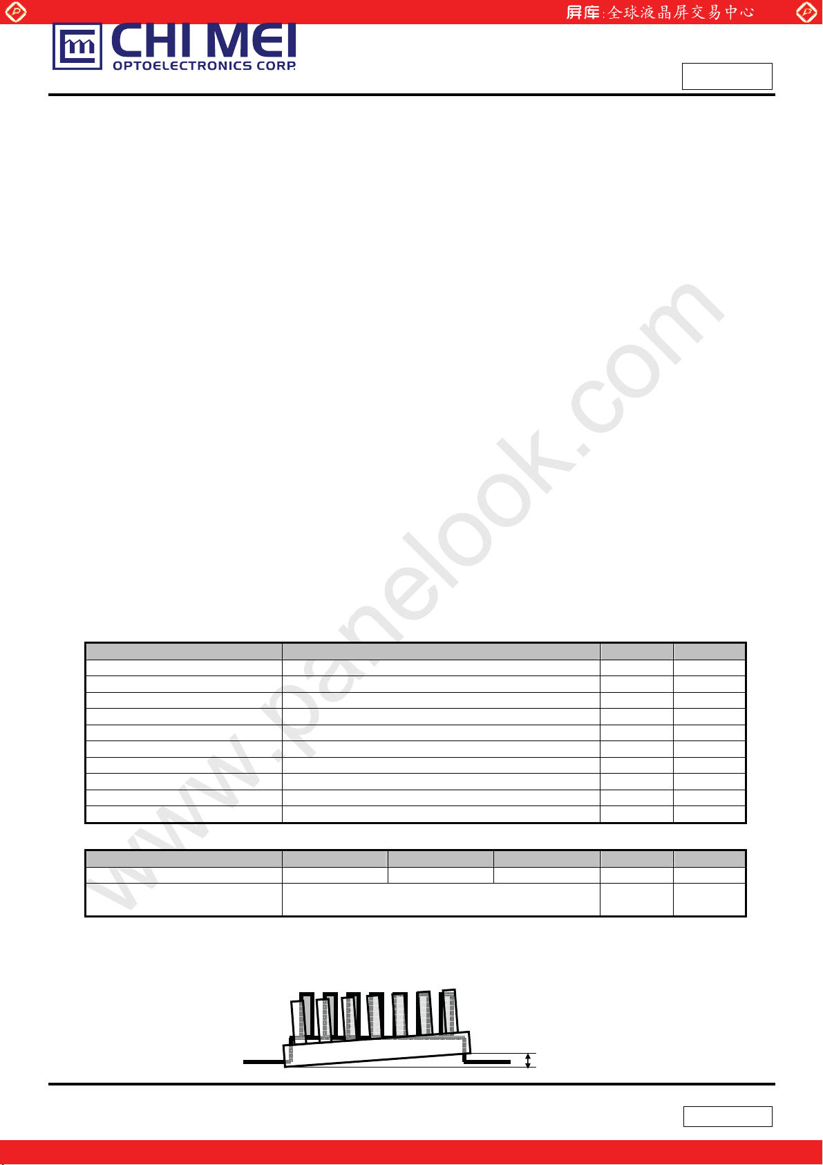
Item Min. Typ. Max. Unit Note
Weight
I/F connector mounting
position
Note (1) Please refer to the attached drawings for more information of front and back outline dimensions.
The mounting inclination of the connector makes
the screen center within ±0.5mm as the horizontal.
-
- 472 g -
- (2)
(2) Connector mounting position
(3) Please refer to sec.3.1 for more information of power consumption.
+/- 0.5mm
4 / 24
One step solution for LCD / PDP / OLED panel application: Datasheet, inventory and accessory!
Version 2.2
www.panelook.com
Page 5
Global LCD Panel Exchange Center
www.panelook.com
Doc No.: 400036776
Issued Date: Feb.05, 2010
Model No.: M190A1-P0G
2. ABSOLUTE MAXIMUM RATINGS
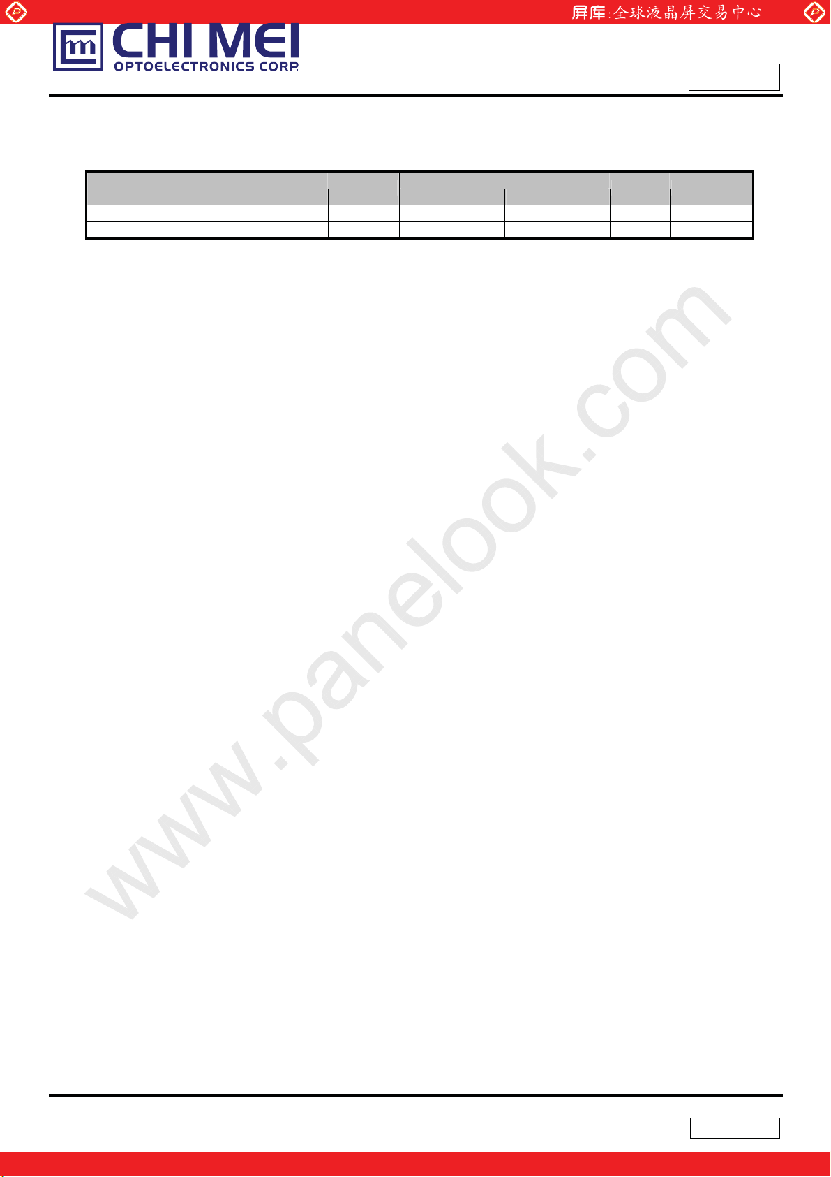
2.1 ABSOLUTE RATINGS OF ENVIRONMENT (BASED ON CMO MODULE M190A1-L0G)
Item Symbol
Storage Temperature TST -20 +60 ºC (1)
Operating Ambient Temperature TOP 0 +50 ºC (1), (2)
Min. Max.
Value
Approval
Unit Note
5 / 24
One step solution for LCD / PDP / OLED panel application: Datasheet, inventory and accessory!
Version 2.2
www.panelook.com
Page 6
Global LCD Panel Exchange Center
www.panelook.com
Doc No.: 400036776
2.2 ABSOLUTE RATINGS OF ENVIRONMENT (OPEN CELL)
High temperature or humidity may reduce the performance of panel. Please store LCD panel within the specified
storage conditions.
Storage Condition: With packing.
Storage temperature range: 25±5 ºC.
Storage humidity range: 50±10%RH.
Shelf life: 30days
2.3 ELECTRICAL ABSOLUTE RATINGS (OPEN CELL)
Issued Date: Feb.05, 2010
Model No.: M190A1-P0G
Approval
Item Symbol
Power Supply Voltage Vcc -0.3 +6.0 V (1)
Logic Input Voltage Vlogic -0.3 3.6 V -
Note (1) Permanent damage might occur if the module is operated at conditions exceeding the maximum values.
Min. Max.
Value
Unit Note
6 / 24
One step solution for LCD / PDP / OLED panel application: Datasheet, inventory and accessory!
Version 2.2
www.panelook.com
Page 7
Global LCD Panel Exchange Center
www.panelook.com
Doc No.: 400036776
Issued Date: Feb.05, 2010
Model No.: M190A1-P0G
3. ELECTRICAL CHARACTERISTICS
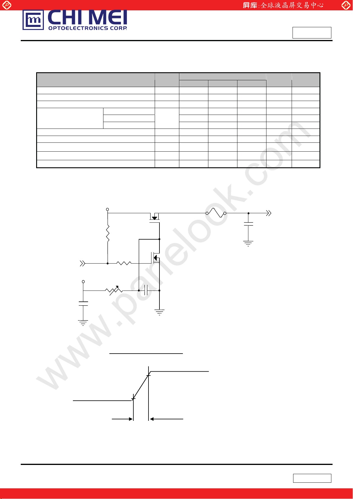
3.1 TFT LCD OPEN CELL Ta = 25 ± 2 ºC
Parameter Symbol
Min. Typ. Max.
Power Supply Voltage Vcc 4.5 5.0 5.5 V Ripple Voltage VRP - - 150 mV Power on Rush Current I
-
RUSH
White - 0.37 0.48 A (3)a
Power Supply Current
Black - 0.71 0.85 A (3)b
Vertical Stripe
lcc
- 0.63 0.75 A (3)c
Power Consumption(without Backlight Unit) PLCD 3.55 4.25 Watt (4)
LVDS differential input voltage Vid 100 - 600 mV -
LVDS common input voltage Vic - 1.2 - V -
Logic High Input Voltage VIH 2.64 - - V Logic Low Input Voltage VIL - - 0.66 V -
Note (1) The module should be always operated within above ranges.
Value
-
Unit Note
3 A (2)
Approval
Note (2) Measurement Conditions:
+5.0V
R1
47K
(High to Low)
(Control Signal)
SW
+12V
47K
VR1
C1
1uF
Vcc rising time is 470μs
Q1 2SK1475
FUSE
R2
1K
0.01uF
Q2
2SK1470
C2
C3
1uF
Vcc
(LCD Module Input)
Vcc
0.9Vcc
0.1Vcc
GND
470μs
7 / 24
One step solution for LCD / PDP / OLED panel application: Datasheet, inventory and accessory!
Version 2.2
www.panelook.com
Page 8
Global LCD Panel Exchange Center
≤≤≤
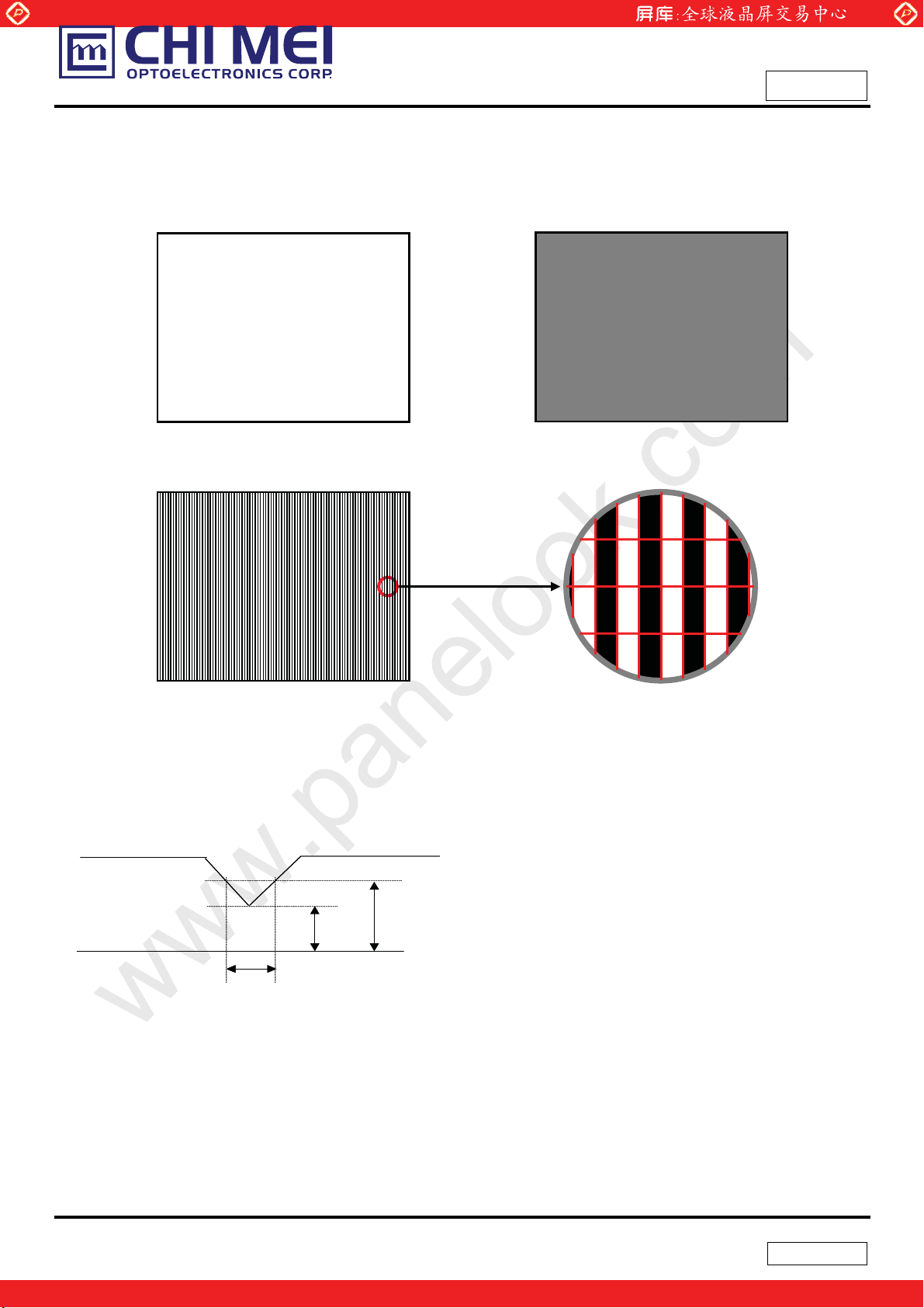
Note (3) The specified power supply current is under the conditions at Vcc = 5.0 V, Ta = 25 ± 2 ºC, fv = 60
Hz, whereas a power dissipation check pattern below is displayed.
www.panelook.com
Doc No.: 400036776
Issued Date: Feb.05, 2010
Model No.: M190A1-P0G
Approval
a. White Pattern
Active Area
c. Vertical Stripe Pattern
b. Black Pattern
Active Area
R
G
R
B
G
R
B
G
R R
G
B
B
B
B
R
R
R
G
G
G
G
B
B
B
B
R
R
Active Area
Note (4) The power consumption is specified at the pattern with the maximum current.
3.2 Vcc POWER DIP CONDITION:
Vcc
Vcc
4.5V
4.5V
4.0V
4.0V
Td
Td
Dip condition:
msTdVVccV 20,5.40.4
8 / 24
One step solution for LCD / PDP / OLED panel application: Datasheet, inventory and accessory!
Version 2.2
www.panelook.com
Page 9
Global LCD Panel Exchange Center
)
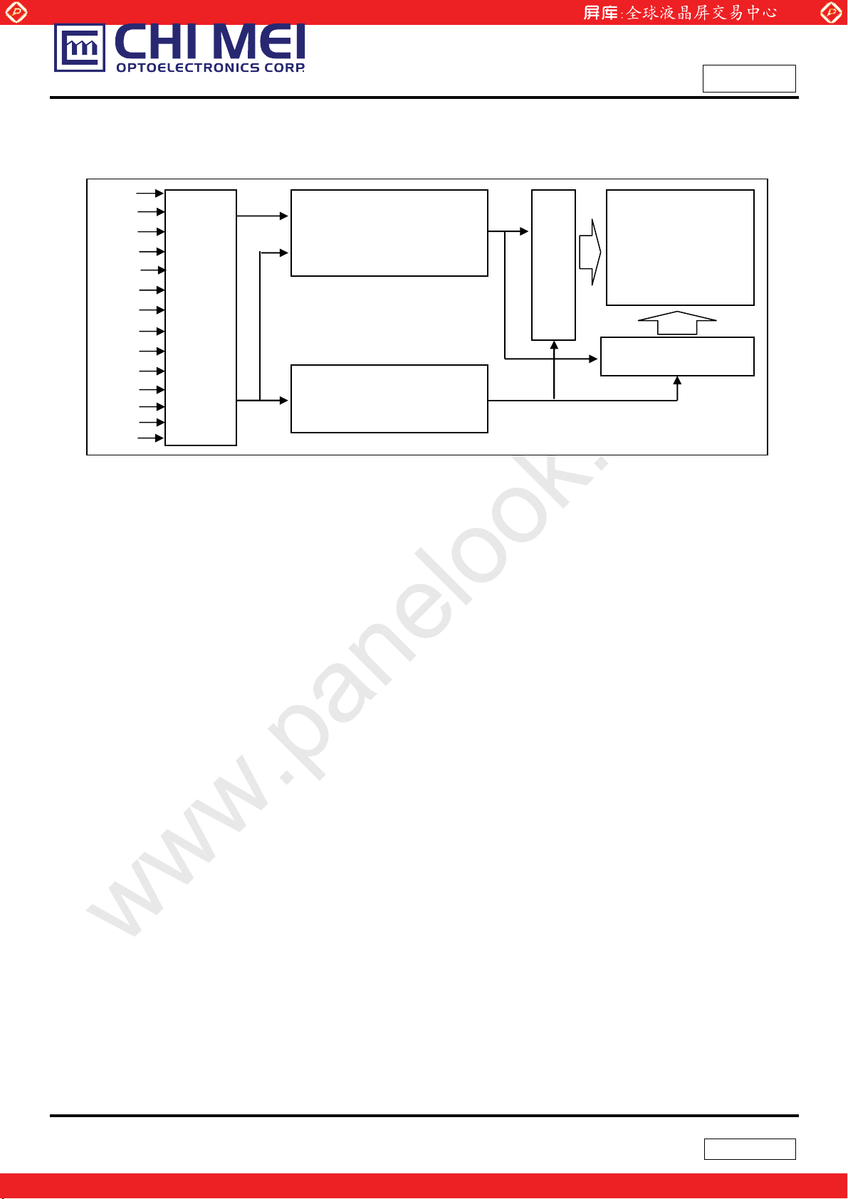
4. BLOCK DIAGRAM
4.1 TFT LCD OPEN CELL
www.panelook.com
Doc No.: 400036776
Issued Date: Feb.05, 2010
Model No.: M190A1-P0G
Approval
RXO0(+/-)
RXO1(+/-)
RXO2(+/-)
RXO3(+/-)
RXOC(+/-)
RXE0(+/-)
RXE1(+/-)
RXE2(+/-)
RXE3(+/-)
RXEC(+/-)
NC
NC/Agmode
Vcc
GND
STM - MSAKT2407P30A
(JAE-FI-X30SSL-HF or
INPUT CONNECTOR
TIMING CONTROLLER
DC/DC CONVERTER &
REFERENCE VOLTAGE
SCAN DRIVER IC
LVDS INPUT /
TFT LCD PANEL
(1440x3x900)
DATA DRIVER IC
9 / 24
One step solution for LCD / PDP / OLED panel application: Datasheet, inventory and accessory!
Version 2.2
www.panelook.com
Page 10
Global LCD Panel Exchange Center
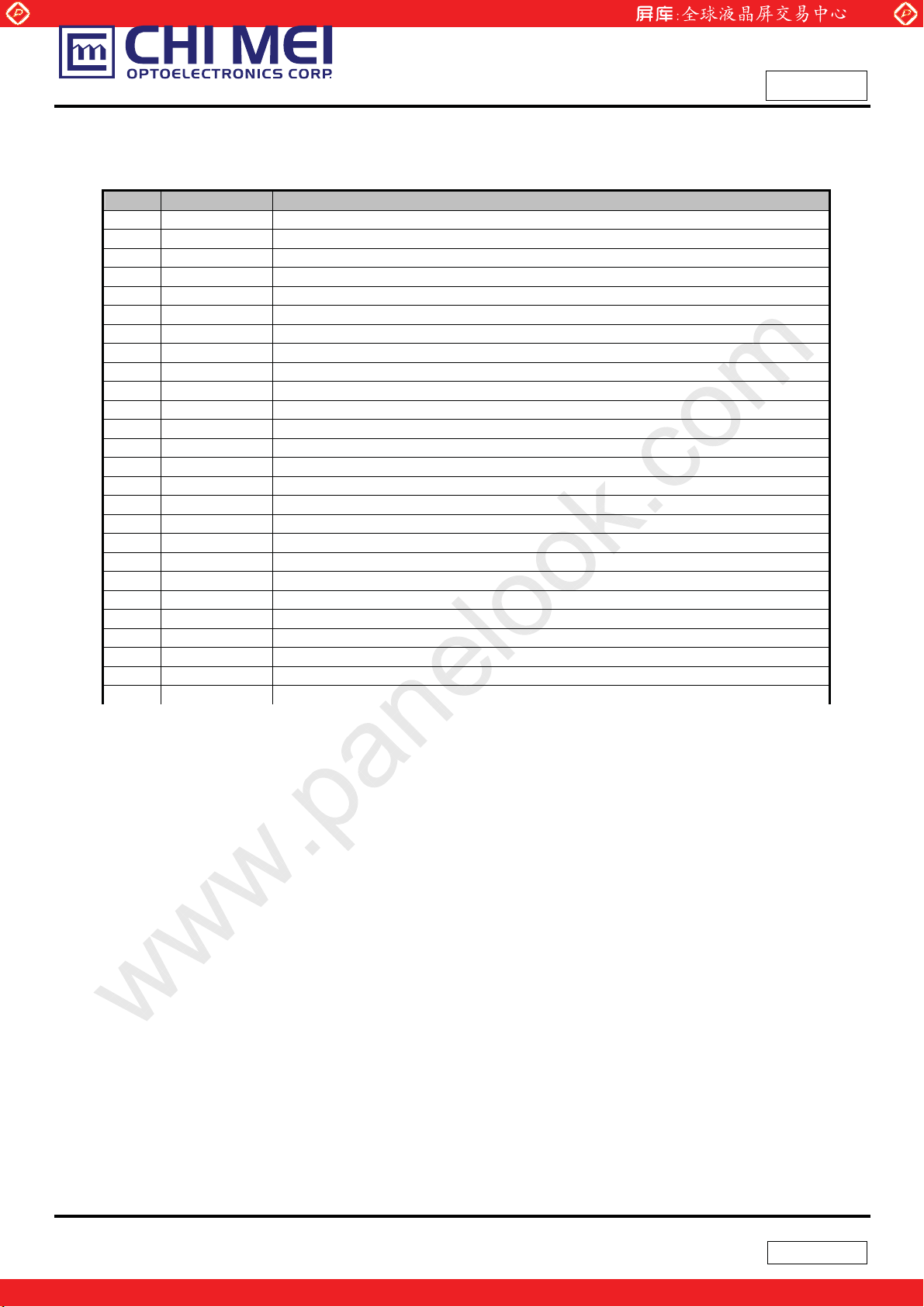
5. INPUT TERMINAL PIN ASSIGNMENT
5.1 TFT LCD MODULE
Pin Name Description
1 RXO0- Negative LVDS differential data input. Channel O0 (odd)
2 RXO0+ Positive LVDS differential data input. Channel O0 (odd)
3 RXO1- Negative LVDS differential data input. Channel O1 (odd)
4 RXO1+ Positive LVDS differential data input. Channel O1 (odd)
5 RXO2- Negative LVDS differential data input. Channel O2 (odd)
6 RXO2+ Positive LVDS differential data input. Channel O2 (odd)
7 GND Ground
8 RXOC- Negative LVDS differential clock input. (odd)
9 RXOC+ Positive LVDS differential clock input. (odd)
10 RXO3- Negative LVDS differential data input. Channel O3(odd)
11 RXO3+ Positive LVDS differential data input. Channel O3 (odd)
12 RXE0- Negative LVDS differential data input. Channel E0 (even)
13 RXE0+ Positive LVDS differential data input. Channel E0 (even)
14 GND Ground
15 RXE1- Negative LVDS differential data input. Channel E1 (even)
16 RXE1+ Positive LVDS differential data input. Channel E1 (even)
17 GND Ground
18 RXE2- Negative LVDS differential data input. Channel E2 (even)
19 RXE2+ Positive LVDS differential data input. Channel E2 (even)
20 RXEC- Negative LVDS differential clock input. (even)
21 RXEC+ Positive LVDS differential clock input. (even)
22 RXE3- Negative LVDS differential data input. Channel E3 (even)
23 RXE3+ Positive LVDS differential data input. Channel E3 (even)
24 GND Ground
25 NC For LCD internal use only, do not connect
26 NC
For LCD internal use only, do not connect
www.panelook.com
Doc No.: 400036776
Issued Date: Feb.05, 2010
Model No.: M190A1-P0G
Approval
10 / 24
One step solution for LCD / PDP / OLED panel application: Datasheet, inventory and accessory!
Version 2.2
www.panelook.com
Page 11
Global LCD Panel Exchange Center
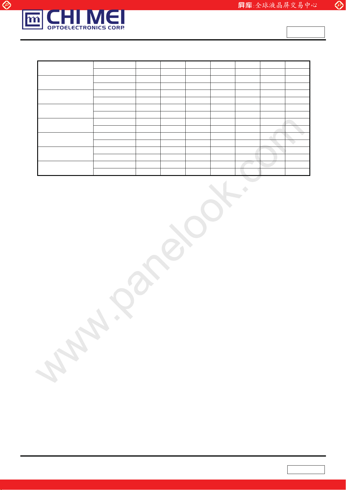
5.2 LVDS DATA MAPPING TABLE
LVDS Channel O0
LVDS Channel O1
LVDS Channel O2
LVDS Channel O3
LVDS Channel E0
LVDS Channel E1
LVDS Channel E2
LVDS Channel E3
LVDS output D7 D6 D4 D3 D2 D1 D0
Data order OG0 OR5 OR4 OR3 OR2 OR1 OR0
LVDS output D18 D15 D14 D13 D12 D9 D8
Data order OB1 OB0 OG5 OG4 OG3 OG2 OG1
LVDS output D26 D25 D24 D22 D21 D20 D19
Data order DE NA NA OB5 OB4 OB3 OB2
LVDS output D23 D17 D16 D11 D10 D5 D27
Data order NA OB7 OB6 OG7 OG6 OR7 OR6
LVDS output D7 D6 D4 D3 D2 D1 D0
Data order EG0 ER5 ER4 ER3 ER2 ER1 ER0
LVDS output D18 D15 D14 D13 D12 D9 D8
Data order EB1 EB0 EG5 EG4 EG3 EG2 EG1
LVDS output D26 D25 D24 D22 D21 D20 D19
Data order DE NA NA EB5 EB4 EB3 EB2
LVDS output D23 D17 D16 D11 D10 D5 D27
Data order NA EB7 EB6 EG7 EG6 ER7 ER6
www.panelook.com
Doc No.: 400036776
Issued Date: Feb.05, 2010
Model No.: M190A1-P0G
Approval
11 / 24
One step solution for LCD / PDP / OLED panel application: Datasheet, inventory and accessory!
Version 2.2
www.panelook.com
Page 12
Global LCD Panel Exchange Center
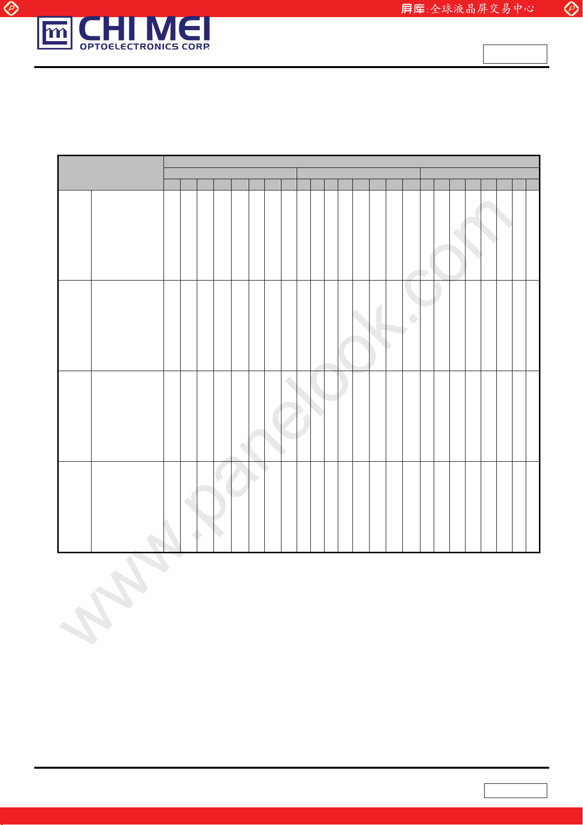
5.3 COLOR DATA INPUT ASSIGNMENT
The brightness of each primary color (red, green and blue) is based on the 8-bit gray scale data input for
the color. The higher the binary input, the brighter the color. The table below provides the assignment of
color versus data input.
Color
R7 R6 R5 R4 R3 R2 R1 R0 R7 R6 G5 G4 G3 G2 G1 G0 R7 R6 B5 B4 B3 B2 B1 B0
Black
Red
Green
Basic
Colors
Gray
Scale
Of
Red
Gray
Scale
Of
Green
Gray
Scale
Of
Blue
Note (1) 0: Low Level Voltage, 1: High Level Voltage
Blue
Cyan
Magenta
Yellow
White
Red(0) / Dark
Red(1)
Red(2)
:
:
Red(253)
Red(254)
Red(255)
Green(0) / Dark
Green(1)
Green(2)
:
:
Green(253)
Green(254)
Green(255)
Blue(0) / Dark
Blue(1)
Blue(2)
:
:
Blue(253)
Blue(254)
Blue(255)
0
0
1
1
0
0
0
0
0
0
1
1
1
1
1
1
0
0
0
0
0
0
:
:
:
:
1
1
1
1
1
1
0
0
0
0
0
0
:
:
:
:
0
0
0
0
0
0
0
0
0
0
0
0
:
:
:
:
0
0
0
0
0
0
www.panelook.com
Doc No.: 400036776
Issued Date: Feb.05, 2010
Model No.: M190A1-P0G
Approval
Data Signal
Red Green Blue
0
0
0
0
0
0
0
0
0
0
0
0
0
0
0
0
0
0
0
0
0
0
1
1
1
1
1
1
0
0
0
0
0
0
0
0
0
0
0
0
0
0
0
0
0
0
0
0
0
0
1
1
1
1
1
1
1
1
0
0
0
0
0
0
0
0
0
0
0
0
0
0
0
0
0
0
0
0
0
0
1
1
1
1
1
1
1
1
0
0
0
0
0
0
1
1
1
1
1
1
1
1
1
1
1
1
1
1
1
1
1
1
1
1
1
1
0
0
0
0
0
0
0
0
1
1
1
1
1
1
1
1
1
1
1
1
1
1
1
1
1
1
1
1
1
1
0
0
0
0
0
0
0
0
1
1
1
1
1
1
1
1
1
1
1
1
1
1
1
1
1
1
1
1
1
1
0
0
0
0
0
0
0
0
0
0
0
0
0
0
0
0
0
0
0
0
0
0
0
0
0
0
0
1
0
0
0
0
0
0
0
0
0
0
0
0
0
0
0
0
0
0
0
0
1
0
0
0
0
0
0
0
0
0
0
0
0
0
0
0
0
0
:
:
:
:
:
:
:
:
:
:
:
:
:
:
:
:
:
:
:
:
:
:
:
:
:
:
:
:
:
:
:
:
:
:
:
:
:
:
:
:
:
:
:
:
1
1
1
1
0
1
0
0
0
0
0
0
0
0
0
0
0
0
0
0
0
0
1
1
1
1
1
0
0
0
0
0
0
0
0
0
0
0
0
0
0
0
0
0
1
1
1
1
1
1
0
0
0
0
0
0
0
0
0
0
0
0
0
0
0
0
0
0
0
0
0
0
0
0
0
0
0
0
0
0
0
0
0
0
0
0
0
0
0
0
0
0
0
0
0
0
0
0
0
0
0
1
0
0
0
0
0
0
0
0
0
0
0
0
0
0
0
0
0
0
0
0
1
0
0
0
0
0
0
0
0
0
:
:
:
:
:
:
:
:
:
:
:
:
:
:
:
:
:
:
:
:
:
:
:
:
:
:
:
:
:
:
:
:
:
:
:
:
:
:
:
:
:
:
:
:
0
0
0
0
0
0
1
1
1
1
1
1
0
1
0
0
0
0
0
0
0
0
0
0
0
0
0
0
1
1
1
1
1
1
1
0
0
0
0
0
0
0
0
0
0
0
0
0
0
0
1
1
1
1
1
1
1
1
0
0
0
0
0
0
0
0
0
0
0
0
0
0
0
0
0
0
0
0
0
0
0
0
0
0
0
0
0
0
0
0
0
0
0
0
0
0
0
0
0
0
0
0
0
0
0
0
0
0
0
1
0
0
0
0
0
0
0
0
0
0
0
0
0
0
0
0
0
0
0
0
1
0
:
:
:
:
:
:
:
:
:
:
:
:
:
:
:
:
:
:
:
:
:
:
:
:
:
:
:
:
:
:
:
:
:
:
:
:
:
:
:
:
:
:
:
:
0
0
0
0
0
0
0
0
0
0
0
0
0
0
1
1
1
1
1
1
0
1
0
0
0
0
0
0
0
0
0
0
0
0
0
0
1
1
1
1
1
1
1
0
0
0
0
0
0
0
0
0
0
0
0
0
0
0
1
1
1
1
1
1
1
1
12 / 24
One step solution for LCD / PDP / OLED panel application: Datasheet, inventory and accessory!
Version 2.2
www.panelook.com
Page 13
Global LCD Panel Exchange Center
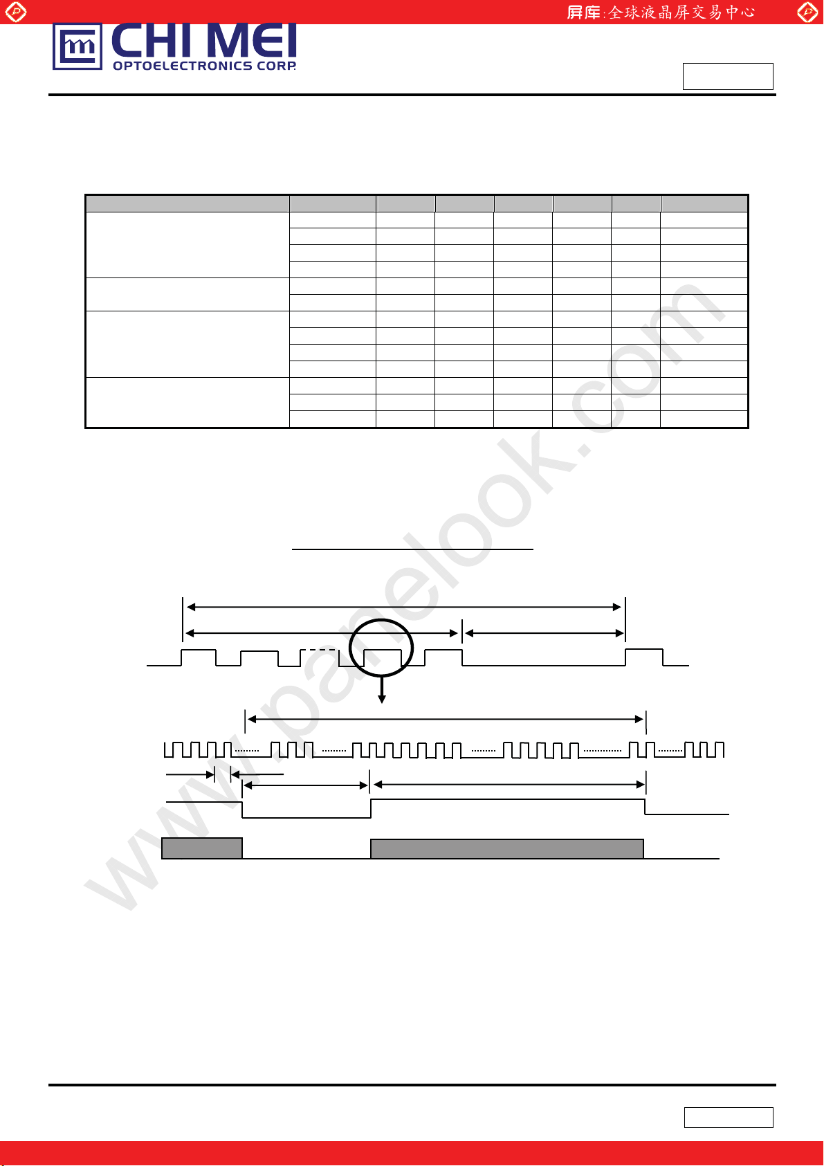
6. INTERFACE TIMING
6.1 INPUT SIGNAL TIMING SPECIFICATIONS
The input signal timing specifications are shown as the following table and timing diagram.
Signal Item Symbol Min. Typ. Max. Unit Note
Frequency Fc 34.8 44.5 75.6 MHz -
LVDS Clock
LVDS Da t a
Vertical Active Display Term
Horizontal Active Display Term
Period Tc 13.2 22.5 28.7 ns
High Time Tch - 4/7 - Tc Low Time Tcl - 3/7 - Tc Setup Time Tlvs 600 - - ps Hold Time Tlvh 600 - - ps Frame Rate Fr 50 60 75 Hz Total Tv 905 926 1050 Th Tv=Tvd+Tvb
Display Tvd 900 900 900 Th Blank Tvb Tv-Tvd 26 Tv-Tvd Th Total Th 770 800 960 Tc Th=Thd+Thb
Display Thd 720 720 720 Tc Blank Thb Th-Thd 80 Th-Thd Tc -
www.panelook.com
Doc No.: 400036776
Issued Date: Feb.05, 2010
Model No.: M190A1-P0G
Approval
Note: Because this module is operated by DE only mode, Hsync and Vsync input signals should be set
to low logic level or ground. Otherwise, this module would operate abnormally.
INPUT SIGNAL TIMING DIAGRAM
DE
Th
DCLK
DE
DATA
TC
Thb
hd
T
13 / 24
One step solution for LCD / PDP / OLED panel application: Datasheet, inventory and accessory!
Version 2.2
www.panelook.com
Page 14
Global LCD Panel Exchange Center
www.panelook.com
Doc No.: 400036776
Issued Date: Feb.05, 2010
Model No.: M190A1-P0G
Approval
14 / 24
One step solution for LCD / PDP / OLED panel application: Datasheet, inventory and accessory!
Version 2.2
www.panelook.com
Page 15
Global LCD Panel Exchange Center
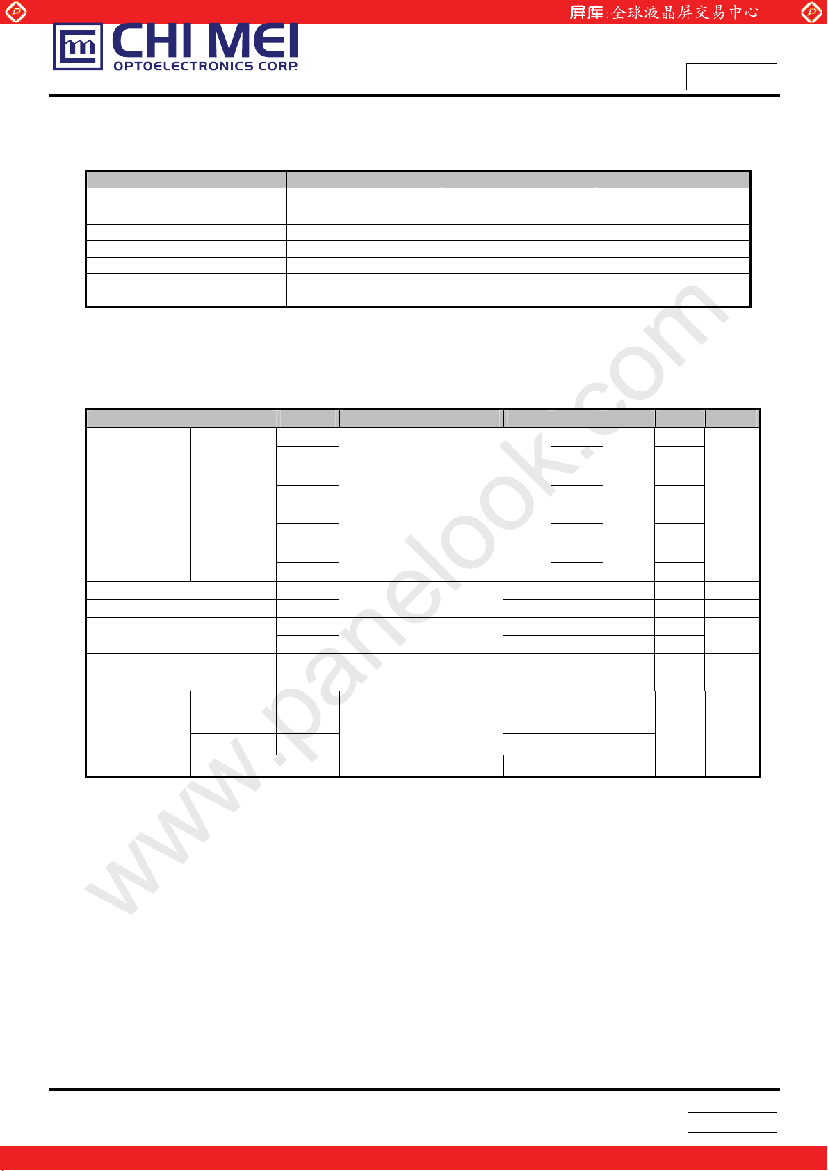
7. OPTICAL CHARACTERISTICS
7.1 TEST CONDITIONS
Item Symbol Value Unit
Ambient Temperature Ta
Ambient Humidity Ha
Supply Voltage VCC 5.0 V
Input Signal According to typical value in "3. ELECTRICAL CHARACTERISTICS"
Inverter Current IL 7.0 mA
Inverter Driving Frequency FL 55 KHz
Inverter Logah MIT 70070.50
7.2 OPTICAL SPECIFICATIONS
The relative measurement methods of optical characteristics are shown as below. The following items
should be measured under the test conditions described in 7.1 and stable environment shown in Note (6).
www.panelook.com
Doc No.: 400036776
Issued Date: Feb.05, 2010
Model No.: M190A1-P0G
Approval
o
25±2
50±10
C
%RH
Item Symbol Condition Min. Typ. Max. Unit Note
Rcx 0.651
Rcy
Gcx 0.274
Gcy
Bcx 0.149
Bcy
Wcx 0.322
Wcy
Color
Chromaticity
Red
Green
Blue
White
Center Transmittance T%
Contrast Ratio CR
T
Response Time
R
T
F
Transmittance uniformity δT
Horizontal
Viewing Angle
Vertica l
θx+ 75 85
θ
x
θY+
θ
Y
θ
=0° , θY =0°
x
CS-1000T
Standard light source “C”
θ
=0° , θY =0°
x
CS-1000T, CMO BLU 700 1000
θx=0° , θY =0°
θ
=0° , θY =0°
x
CS-1000T
-
CR≥10
BM-5A
-
-
0.328
-
-
Typ -
0.03
0.594
0.108
Typ +
0.03
-
-
-
-
0.363
-
6.1 6.8 - %
-
-
-
1.5 2.5 ms
3.5 5.5 ms
- (1), (3)
- 1.25 1.4 -
-
75
70
70
85
80
80
-
Deg.
-
-
(0),(6)
(1), (8)
(4)
(1), (7)
(1), (2)
(6)
15 / 24
One step solution for LCD / PDP / OLED panel application: Datasheet, inventory and accessory!
Version 2.2
www.panelook.com
Page 16
Global LCD Panel Exchange Center
www.panelook.com
Doc No.: 400036776
Issued Date: Feb.05, 2010
Model No.: M190A1-P0G
Approval
16 / 24
One step solution for LCD / PDP / OLED panel application: Datasheet, inventory and accessory!
Version 2.2
www.panelook.com
Page 17
Global LCD Panel Exchange Center
s
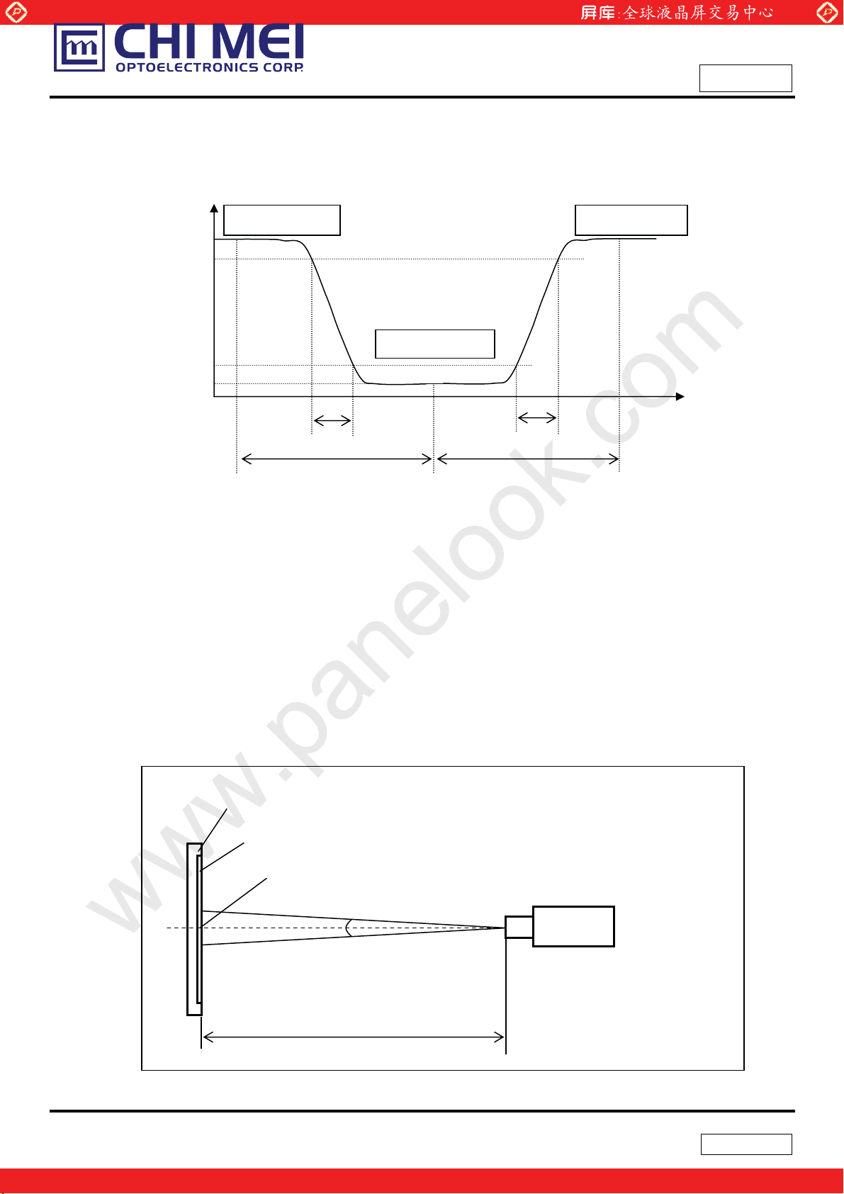
Note (4) Definition of Response Time (TR, TF):
www.panelook.com
Doc No.: 400036776
Issued Date: Feb.05, 2010
Model No.: M190A1-P0G
Approval
100%
90%
Optical
Response
10%
0%
Gray Level 255
T
R
66.67 m
Note (5) Definition of Luminance of White (L
Measure the luminance of gray level 255 at center point
L
= L (1)
C
L (x) is corresponding to the luminance of the point X at Figure in Note (7).
Gray Level 255
Time
T
F
66.67 ms
):
C
Note (6) Measurement Setup:
The LCD module should be stabilized at given temperature for 20 minutes to avoid abrupt
temperature change during measuring. In order to stabilize the luminance, the measurement
should be executed after lighting Backlight for 20 minutes in a windless room.
LCD Module
LCD Panel
Center of the Screen
Field of View = 2º
500 mm
CS-1000T
Light Shield Room
(Ambient Luminance < 2 lux)
17 / 24
One step solution for LCD / PDP / OLED panel application: Datasheet, inventory and accessory!
Version 2.2
www.panelook.com
Page 18
Global LCD Panel Exchange Center
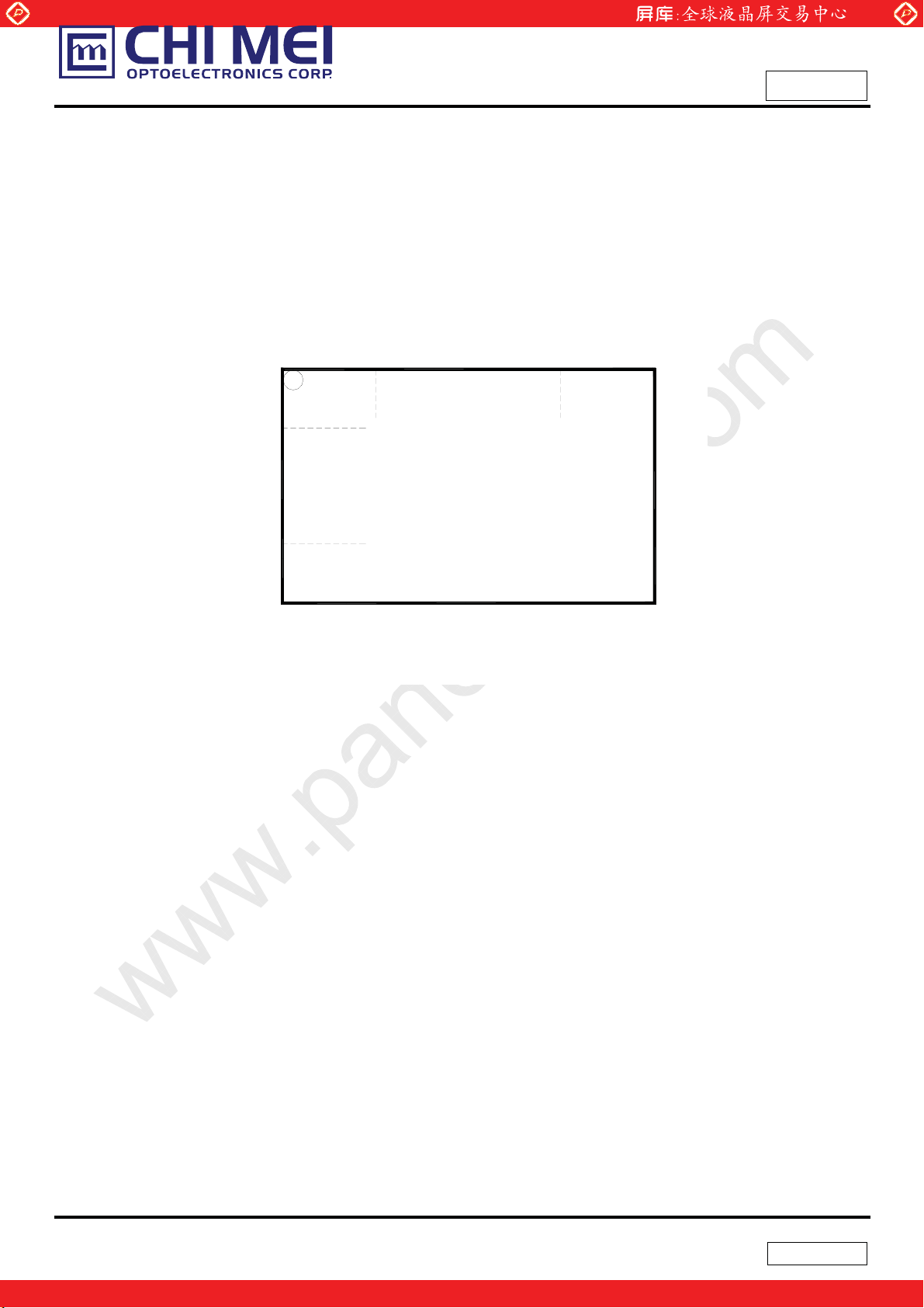
Note (7) Definition of Transmittance Variation (δT):
Measure the transmittance at 13 points
δT =
www.panelook.com
Doc No.: 400036776
Issued Date: Feb.05, 2010
Model No.: M190A1-P0G
Approval
18 / 24
One step solution for LCD / PDP / OLED panel application: Datasheet, inventory and accessory!
Version 2.2
www.panelook.com
Page 19
Global LCD Panel Exchange Center
7.3 Flicker Adjustment
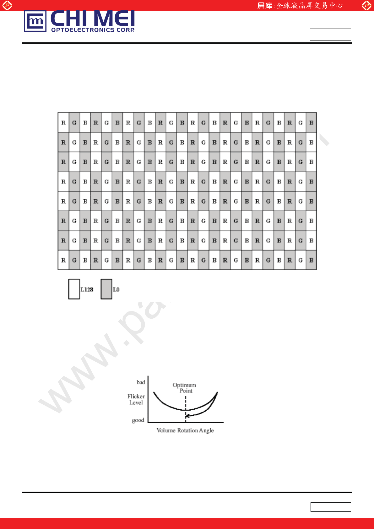
Flicker must be finely adjusted after module assembling and aging. Please follow the instructions below.
(1) Adjustment Pattern: 2H1V checker pattern as follows.
www.panelook.com
Doc No.: 400036776
Issued Date: Feb.05, 2010
Model No.: M190A1-P0G
Approval
(2) Adjustment Method:
Flicker should be adjusted by turning the volume for flicker adjustment by the ceramic driver. It is adjusted
to the point with least flickering of the whole screen. After making it surely overrun at once, it should be
adjusted to the optimum point.
19 / 24
One step solution for LCD / PDP / OLED panel application: Datasheet, inventory and accessory!
Version 2.2
www.panelook.com
Page 20
Global LCD Panel Exchange Center
Doc No.: 400036776
8. PACKAGING
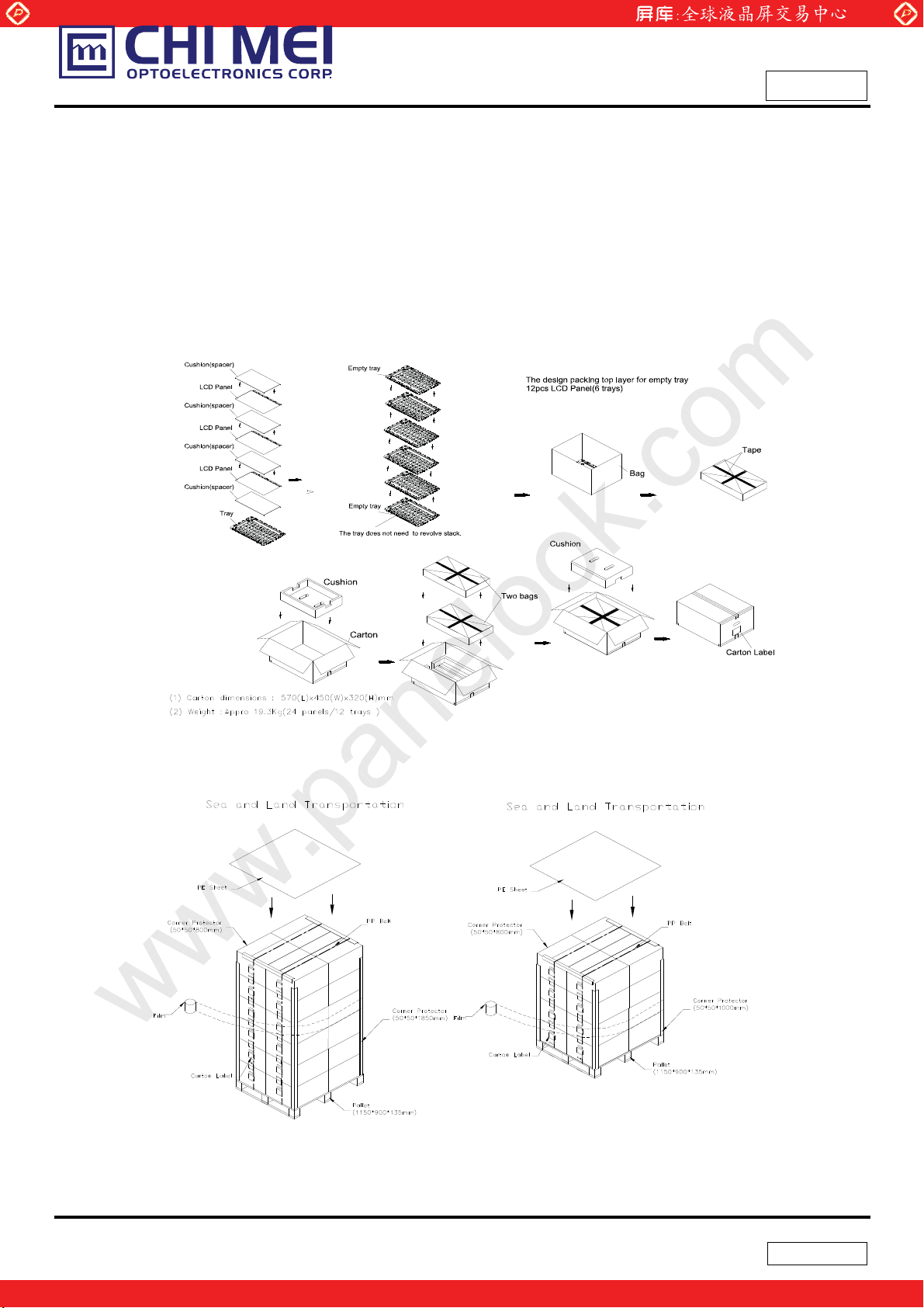
8.1 PACKING SPECIFICATIONS
(1) 24 open cells / 1 Box
(2) Box dimensions: 570 (L) X 450 (W) X 320 (H) mm
(3) Weight: approximately 19.3Kg (24 open cells per box)
8.2 PACKING METHOD
www.panelook.com
Issued Date: Feb.05, 2010
Model No.: M190A1-P0G
Approval
20 / 24
One step solution for LCD / PDP / OLED panel application: Datasheet, inventory and accessory!
Version 2.2
www.panelook.com
Page 21
Global LCD Panel Exchange Center
9. DEFINITION OF LABELS
9.1 CMO OPEN CELL LABEL
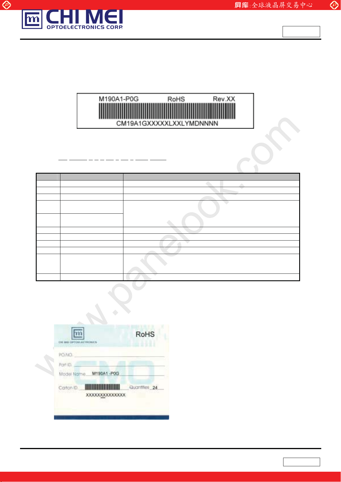
The barcode nameplate is pasted on each OPEN CELL as illustration for CMO internal control.
Barcode definition:
www.panelook.com
Doc No.: 400036776
Issued Date: Feb.05, 2010
Model No.: M190A1-P0G
Approval
Serial ID: CM
Code Meaning Description
CM Supplier code CMO=CM
19A1G Model number M190A1-P0G=19A1G
X Revision code C1:1, C2:2, …
X Source driver IC code
X Gate driver IC code
XX Cell location Tainan, Taiwan=TN
L Cell line # 0~12=1~C
XX Module location Tainan, Taiwan=TN
L Module line # 0~12=1~C
YMD Year, month, day
NNNN Serial number Manufacturing sequence of product
-19A1G-X-X-X-XX-L-XX-L-YMD-NNNN
Century=1, CLL=2, Demos=3, Epson=4, Fujitsu=5, Himax=6,
Hitachi=7, Hynix=8, LDI=9, Matsushita=A, NEC=B, Novatek=C,
OKI=D, Philips=E, Renasas=F, Samsung=G, Sanyo=H, Sharp=I,
TI=J, Topro=K, Toshiba=L, Windbond=M
Year: 2001=1, 2002=2, 2003=3, 2004=4…
Month: 1~12=1, 2, 3, ~, 9, A, B, C
Day: 1~31= 1, 2, 3, ~, 9, A, B, C, ~, T, U, V
9.2 CARTON LABEL
The barcode nameplate is pasted on each box as illustration, and its definitions are as following explanation.
(a) Model Name: M190A1 –P0G
(b) Carton ID: CMO internal control
(c) Quantities: 24 pcs
21 / 24
One step solution for LCD / PDP / OLED panel application: Datasheet, inventory and accessory!
Version 2.2
www.panelook.com
Page 22
Global LCD Panel Exchange Center
10. RELIABILITY TEST
Environment test conditions are listed as following table.
Items Required Condition Note
www.panelook.com
Doc No.: 400036776
Issued Date: Feb.05, 2010
Model No.: M190A1-P0G
Approval
22 / 24
One step solution for LCD / PDP / OLED panel application: Datasheet, inventory and accessory!
Version 2.2
www.panelook.com
Page 23
Global LCD Panel Exchange Center
11. PRECAUTIONS
11.1 ASSEMBLY AND HANDLING PRECAUTIONS
(1) Do not apply rough force such as bending or twisting to the product during assembly.
(2) To assemble backlight or install module into user’s system can be only in clean working areas. The dust
and oil may cause electrical short or worsen the polarizer.
(3) It is not permitted to have pressure or impulse on the module because the LCD panel will be damaged.
(4) Always follow the correct power sequence when the product is connecting and operating. This can prevent
damage to the CMOS LSI chips during latch-up.
(5) Do not pull the I/F connector in or out while the module is operating.
(6) Use a soft dry cloth without chemicals for cleaning, because the surface of polarizer is very soft and easily
scratched.
(7) It is dangerous that moisture come into or contacted the product, because moisture may damage the
www.panelook.com
Doc No.: 400036776
Issued Date: Feb.05, 2010
Model No.: M190A1-P0G
Approval
product when it is operating.
(8) High temperature or humidity may reduce the performance of module. Please store this product within the
specified storage conditions.
(9) When ambient temperature is lower than 10ºC may reduce the display quality. For example, the response
time will become slowly.
11.2 SAFETY PRECAUTIONS
(1) If the liquid crystal material leaks from the panel, it should be kept away from the eyes or mouth. In case of
contact with hands, skin or clothes, it has to be washed away thoroughly with soap.
(2) After the product’s end of life, it is not harmful in case of normal operation and storage.
11.3 OTHER
(1) When fixed patterns are displayed for a long time, remnant image is likely to occur.
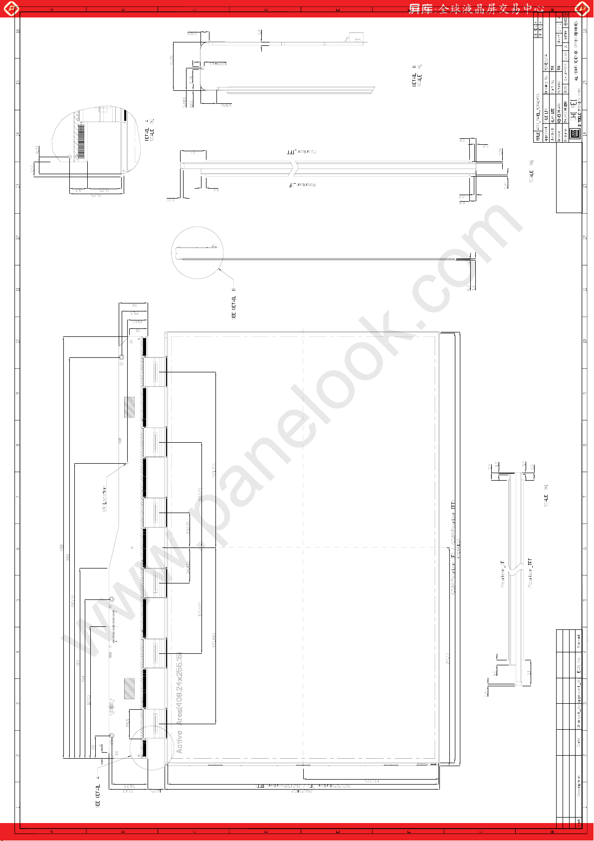
12. MECHANICAL DRAWING
23 / 24
One step solution for LCD / PDP / OLED panel application: Datasheet, inventory and accessory!
Version 2.2
www.panelook.com
Page 24
Global LCD Panel Exchange Center
www.panelook.com
One step solution for LCD / PDP / OLED panel application: Datasheet, inventory and accessory!
www.panelook.com
 Loading...