

Page 1
Global LCD Panel Exchange Center
ಖᙕ
ՠ܂
ᐉு
ߡۥ
ދป
A
TFT LCD Approval Specification
MODEL NO.:M190A1-C01
www.panelook.com
Doc. No.: 1406X054
Issued Date: May.11 2007
Model No.: M190A1-C01
Approval
Customer :
pproved by :
Note :
2007-05-17
10:17:19 CST
2007-05-14
20:35:41 CST
Approve by Dept.
Mgr.(QA RA)
Approve by Director
raymond_lin(ࣥᅩࣧ
/42690)
cs_lee(ޕݳᆣ
/56510/44926)
Department
Manager(QA RA)
Director Accept
/16
1
Version 2.1
One step solution for LCD / PDP / OLED panel application: Datasheet, inventory and accessory!
Accept
www.panelook.com
Page 2
Global LCD Panel Exchange Center
www.panelook.com
Doc. No.: 1406X054
Issued Date: May.11 2007
Model No.: M190A1-C01
Approval
- CONTENTS -
.
REVISION HISTORY ------------------------------------------------------- 3
1. GENERAL DESCRIPTION ------------------------------------------------------- 4
1.1 OVERVIEW
1.2 FEATURES
1.3 APPLICATION
1.4 GENERAL SPECIFICATIONS
2. ABSOLUTE MAXIMUM RATINGS ---------------------------------------------- 4
3. SUGGESTIVE DRIVING CONDITION ---------------------------------------------- 5
4. PANEL PIN DEFINITION ------------------------------------------------------- 6
5. OPTICAL CHARACTERISTICS ---------------------------------------------- 8
5.1 TEST CONDITIONS
5.2 OPTICAL SPECIFICATIONS
6. PACKAGING --------------------------------------------- 12
6.1 PACKING SPECIFICATIONS
6.2 PACKING METHOD
7. DEFINITION OF LABELS ---------------------------------------------- 14
8. PRECAUTIONS ---------------------------------------------- 15
8.1 ASSEMBLY AND HANDLING PRECAUTIONS
8.2 SAFETY PRECAUTIONS
9. PANEL DRAWING ---------------------------------------------- 16
/16
2
Version 2.1
One step solution for LCD / PDP / OLED panel application: Datasheet, inventory and accessory!
www.panelook.com
Page 3
Global LCD Panel Exchange Center
www.panelook.com
REVISION HISTORY
Version Date Section Description
Doc. No.: 1406X054
Issued Date: May.11 2007
Model No.: M190A1-C01
Approval
Ver 2.0
2.1
Sep,18 ’06
May,11 ‘07
-
M190A1-C01 Specifications was first issuedΖ
4
Update Item4
7
20pcs/dense packÆ19pcs/dense pack
/16
3
Version 2.1
One step solution for LCD / PDP / OLED panel application: Datasheet, inventory and accessory!
www.panelook.com
Page 4
Global LCD Panel Exchange Center
www.panelook.com
Doc. No.: 1406X054
Issued Date: May.11 2007
Model No.: M190A1-C01
Approval
1.GENERAL DESCRIPTION
1.1 OVERVIEW
The M190A1-C01 is a 19-inch wide LCD cell with thin film transistors as active elements and contains
1440x900 pixels. Each pixel is divided into red, green and blue dot, which are arranged in vertical stripe.
The cell is normally white mode, and can be applied to the transmission type display. Backlight unit (BLU)
and circuit board for the cell are not built in.
1.2 FEATURES
- Wide viewing angle
- High contrast ratio
- Fast response time
- WXGA+ (1440 x 900 pixels) resolution
1.3 APPLICATION
- LCD Monitor
- LCD TV
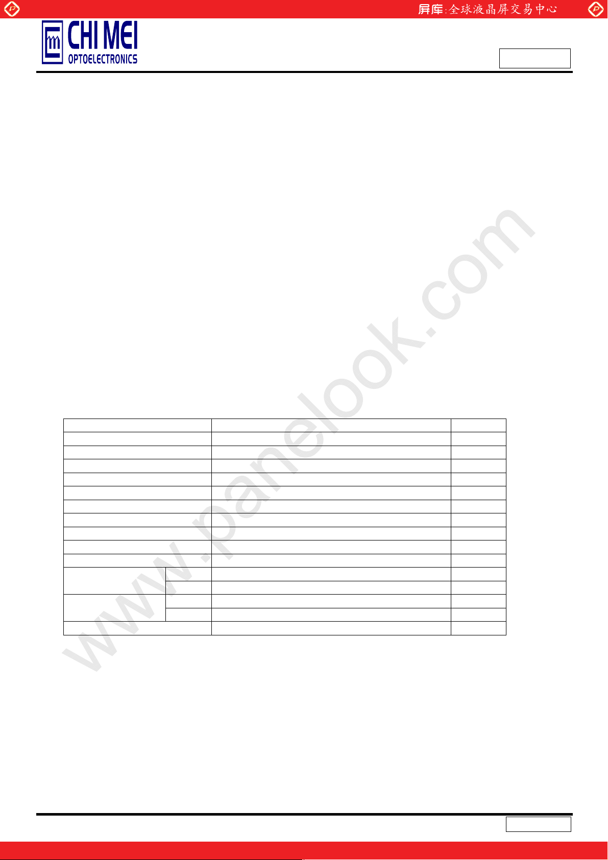
1.4 GENERAL SPECIFICATIONS
Item Specification Unit
Max Panel Dimension (TFT) 419.84 X 266.05 mm
Glass thickness( TFT/ CF ) 0.7/0.7 mm
Active Area 410.4 (H) x 256.5 (V) (19.05” diagonal) mm
Driver Element a-si TFT active matrix Pixel Number 1440X R.G.B X 900 pixel
Pixel Pitch 0.285 (H) X 0.285 (V) mm
Pixel Arrangement RGB vertical stripe Transmissive Mode Normally white Surface Treatment Hard coating (3H), AG (Haze 25%) Polarizer Type E -Wide View -
Polarizer Dimension
Polarizer Thickness
Weight 446(typ.) g
TFT 414.0 X 259.7 mm
CF 415.84 X 262.15 mm
TFT 0.21 mm
CF 0.21 mm
2. ABSOLUTE MAXIMUM RATINGS
1. Storage condition : With shipping package.
2. Storage temperature range : 25±5 к.
3. Storage humidity range : 50±10% RH.
4. Shelf life : 30 days
Version 2.1
/16
4
One step solution for LCD / PDP / OLED panel application: Datasheet, inventory and accessory!
www.panelook.com
Page 5
Global LCD Panel Exchange Center
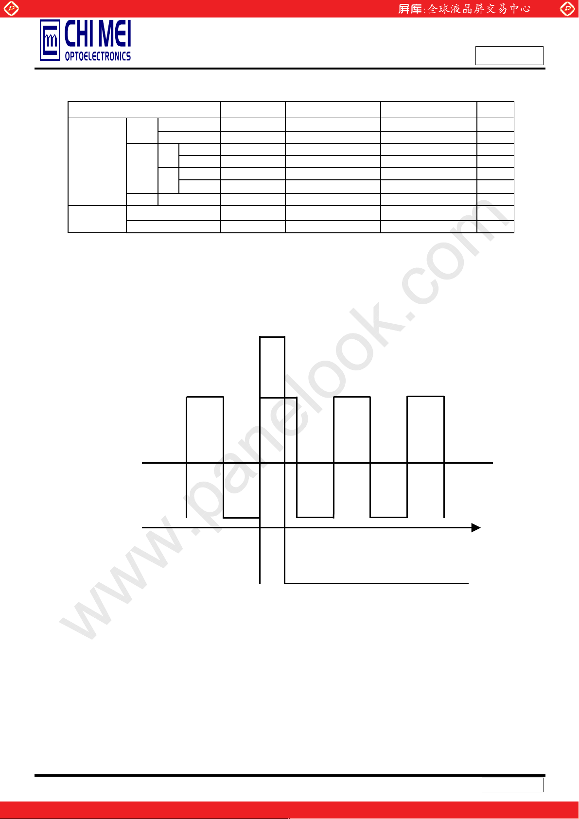
3. Suggestive Driving Condition
Item Min. Typ. Max. Unit
VG
Driving
Voltage
B: Black pattern
W: White pattern
Gamma Voltage : Gam1 > Gam2 > Gam3 > … > Gam10 GЦ: gate pulse falling edge
VD
V
GЦ-D offset
Charging time - 12.43 - us
On 23.7 24.5 25.3 V
Off -6.6 -6.8 -7.0 V
Gam1 - 11.722 - V
B
Gam14 - 0.187 - V
Gam7 - 6.397 - V
W
Gam8 - 5.993 - V
Center - 5.16 - V
COM
www.panelook.com
Doc. No.: 1406X054
Issued Date: May.11 2007
Model No.: M190A1-C01
Approval
2 - - us
DRIVING TIMING DIAGRAM
VG
VD
VCOM
/16
5
Version 2.1
One step solution for LCD / PDP / OLED panel application: Datasheet, inventory and accessory!
www.panelook.com
Page 6

Global LCD Panel Exchange Center
www.panelook.com
4. PANEL PIN DEFINITION
4.1 DATA PIN DEFINE
pin number TAB1 TAB2~9 TAB10
1
2
3
4
5
6
7
8
9
10
11
12
13
14
15
16
17
18
19
20
21
22
23
24
25
26~457
458
459
460
461
462
463
464
465
466
467
468
469
Note: Test pin is recommand for floating
Test Test Test
Test Test Test
Test dummy dummy
XAO dummy dummy
OE dummy dummy
CPV dummy dummy
STV2 dummy dummy
VSS dummy dummy
˩˦˦ʳ
˩˗˗ʳ
˩˗˗ʳ
˩˸˸ʳ
dummy dummy
dummy dummy
dummy dummy
dummy dummy
Vgl dummy dummy
Vgl dummy dummy
˩˺˿ʳ
˩˺˿ʳ
dummy dummy
dummy dummy
˷ʳ ˷ʳ ˷ʳ
˩˺˻ʳ
˩˺˻ʳ
dummy dummy
dummy dummy
Vgh dummy dummy
˩˺˻ʳ
dummy dummy
˷ʳ ˷ʳ ˷ʳ
Vst dummy dummy
˩˶ʳ ˩˶ʳ ˩˶ʳ
Test Test Test
ˢ˨˧˄ˇˆ˅ʳ ˢ˨˧˄ˇˆ˅ʳ ˢ˨˧˄ˇˆ˅ʳ
Test Test Test
dummy dummy Test
˩˶ʳ ˩˶ʳ ˩˶ʳ
dummy dummy Vst
dummy dummy Vgl
dummy dummy Vcom
dummy dummy Vcom
dummy dummy Test
Vcom Vcom Vcom
Vcom Vcom Vcom
Test Test Test
Test Test Test
Doc. No.: 1406X054
Issued Date: May.11 2007
Model No.: M190A1-C01
Approval
/16
6
Version 2.1
One step solution for LCD / PDP / OLED panel application: Datasheet, inventory and accessory!
www.panelook.com
Page 7

Global LCD Panel Exchange Center
4.2 SCAN PIN DEFINE
www.panelook.com
Doc. No.: 1406X054
Issued Date: May.11 2007
Model No.: M190A1-C01
Approval
Scan 1~3
ʳʳʳʳʳʳʳʳʳʳʳ
OE
CPV
STV2
VGL
VSS
VDD
VEE
Vgl
Vgl
DUMMY
ʳʳʳʳʳʳʳʳʳʳVGL
XAO ʳ ʳ VGL
MODE ʳ ʳ VGH
Vdd ʳ ʳ VGH
TEST ʳ ʳ VGH
TEST ʳ ʳ VGH
ʳ ʳ Dummy PAD
DUMMY ʳ ʳ OUT300
. ʳ ʳ .
. ʳ ʳ .
ʳ ʳ .
ʳ ʳ .
. ʳ ʳ .
. ʳ ʳ .
. ʳ ʳ .
. ʳ ʳ .
. ʳ ʳ .
. ʳ ʳ .
. ʳ ʳ .
ʳ ʳ .
ʳ ʳ .
ʳ ʳ .
. ʳ ʳ .
. ʳ ʳ .
. ʳ ʳ .
. ʳ ʳ .
. ʳ ʳ .
DUMMY ʳ ʳ OUT1
ʳ ʳ Dummy PAD
TEST ʳ ʳ VGH
TEST ʳ ʳ VGH
VSS ʳ ʳ VGH
TEST ʳ ʳ VGH
XAO ʳ ʳ VGL
ʳʳʳʳʳʳʳʳʳʳVGL
OE
CPV
VGL
STV1
VSS
VDD
VEE
Vgl
Vgl
DUMMY
/16
7
Version 2.1
One step solution for LCD / PDP / OLED panel application: Datasheet, inventory and accessory!
www.panelook.com
Page 8

Global LCD Panel Exchange Center
5. OPTICAL CHARACTERISTICS
5.1 TEST CONDITIONS
Item Symbol Value Unit
Ambient Temperature Ta
Ambient Humidity Ha
Gamma voltage - Refer to Item 3 driving condition V
Vcom - most suitable Vcom V
5.2 OPTICAL SPECIFICATION
ITEM Symbol Condition MIN. TYP. MAX. UNIT NOTE
Contrast Ratio
Response Time
(Black/White)
Center point Transmittance T%
Transmittance uniformity
(13pts)
Horizontal x
Viewing
Angle
Color
Coordinate
at center
point
(y=0± )
Verti ca l y
(x=0± )
Red
Green
Blue
White
www.panelook.com
Doc. No.: 1406X054
Issued Date: May.11 2007
Model No.: M190A1-C01
Approval
o
25r2
50r10
CR
Tr x=y=0±
Tf x=y=0±
ӬT%
Right
Left 75
Up 70
Down
Rcx x=y=0± 0.649 Rcy x=y=0± 0.332 Gcx x=y=0± 0.274 Gcy x=y=0± 0.589 Bcx x=y=0± 0.148 -
Bcy x=y=0± 0.101 Wcx x=y=0± 0.320 Wcy x=y=0±
x=y=0±
CS-1000T
x=y=0±
CS-1000T
x=y=0± - 1.25 1.4 - 6,1
CR≧10
BM-5A
600 850
--- 1.5 6.5
--- 3.5 8.5
5.4 6.0 - % 7,1
75 85
85
80
70
Typ
-0.03
80
0.356
- % 4,1
- Deg
- Deg
- Deg
- Deg
Typ
+0.03
C
%RH
ms 5,1
ms
2,3,1
2,0
-
Note (0)
Light source is the standard light source “C” which is defined by CIE and driving voltages are based on
suitable gamma voltages. The calculating method is as following:
1.Measure Module’s and BLU’s spectrums. White is without signal input and R, G, B are with signal input.
BLU is supplied by CMO.
2.Calculate cell’s spectrum.
3.Calculate cell’s chromaticity by using the spectrum of standard light source “C”
/16
8
Version 2.1
One step solution for LCD / PDP / OLED panel application: Datasheet, inventory and accessory!
www.panelook.com
Page 9

Global LCD Panel Exchange Center
www.panelook.com
Doc. No.: 1406X054
Issued Date: May.11 2007
Model No.: M190A1-C01
Approval
Note (1)
Light source is the BLU which is supplied by CMO and driving voltages are based on suitable gamma
voltages. White is without signal input and R, G, B are with signal input. SPEC is judged by CMO’s golden sample .
Note (2) : Measurement setup:
The LCD module should be stabilized at given temperature for 20 minutes to avoid abrupt temperature
change during measuring. In order to stabilize the luminance, the measurement should be executed after lighting
backlight for 20 minutes in a windless room.
LCD Module
LCD Panel
USB2000
Center of the Screen
500 mm
CS-1000T
Field of View = 2º
Light Shield Room
(Ambient Luminance < 2 lux)
/16
9
Version 2.1
One step solution for LCD / PDP / OLED panel application: Datasheet, inventory and accessory!
www.panelook.com
Page 10

Global LCD Panel Exchange Center
Note (3) : Definition of viewing angle (x ,y):
www.panelook.com
Doc. No.: 1406X054
Issued Date: May.11 2007
Model No.: M190A1-C01
Approval
Note (4) : Definition of Contrast Ratio (CR):
Ratio of gray max (Gmax), gray min (Gmin), at the center point of panel.
Luminance with all pixel white (Gmax)
CR =
Luminance with all pixel Black (Gmin)
Note (5) : Definition of Response Time (T
100%
90%
Optical
Response
10%
0%
Gray Level 255
R, TF):
T
R
Gray Level 0
Gray Level 255
Time
T
F
66.67ms
/16
10
66.67ms
Version 2.1
One step solution for LCD / PDP / OLED panel application: Datasheet, inventory and accessory!
www.panelook.com
Page 11

Global LCD Panel Exchange Center
Note (6) : Definition of Transmittance Variation (GT%):
Measure the transmittance at 13 points
T% =
δ
Maximum [T%(1), T%(2), … T%(13)]
Minimum [T%(1), T%(2), … T%(13)]
www.panelook.com
Doc. No.: 1406X054
Issued Date: May.11 2007
Model No.: M190A1-C01
Approval
D/10
W
W/10
W/4
W/2
3W/4
Vertical Line
6
9
9W/10
11 12 13
Note (7) : Definition of Transmittance(T%):
Module is without signal input.
BLU is Supplied by CMO .
D
D/4 D/2 3D/4
7
2 3
1
4
Active Area
5
9D/10
8
10
X
: Test Point
X=1 to 13
Transmittance
Luminance of LCD module
=
Ϡ 100%
Luminance of backlight
/16
11
Version 2.1
One step solution for LCD / PDP / OLED panel application: Datasheet, inventory and accessory!
www.panelook.com
Page 12

Global LCD Panel Exchange Center
6. PACKAGING
6.1.PACKING SPECIFICATION
1. 20 pcs LCD panel / 1 Box
2. Box Dimension :472 (L) X376 (W) X 617(H) mm
3. Weight : Approximately 26.9Kg (40 cells per Carton)
6.2 PACKING METHOD
www.panelook.com
W
9
1
Doc. No.: 1406X054
Issued Date: May.11 2007
Model No.: M190A1-C01
Approval
W
9
1
W
9
1
W
9
1
W
9
1
Figure. 6-1 Packing method
]
/16
12
Version 2.1
One step solution for LCD / PDP / OLED panel application: Datasheet, inventory and accessory!
www.panelook.com
Page 13

Global LCD Panel Exchange Center
www.panelook.com
Doc. No.: 1406X054
Issued Date: May.11 2007
Model No.: M190A1-C01
Approval
Figure. 6-2 Packing method
/16
13
Version 2.1
One step solution for LCD / PDP / OLED panel application: Datasheet, inventory and accessory!
www.panelook.com
Page 14

Global LCD Panel Exchange Center
7. DEFINITION OF LABEL
1. Mode Name: M190A1- C01
2. Panel Type: version control
3. Quantity: 19pcs / PP box
4. Case ID: serial number.
5. Note: Notification, if necessary.
6. Barcode: Case ID in code39 format
www.panelook.com
Doc. No.: 1406X054
Issued Date: May.11 2007
Model No.: M190A1-C01
Approval
Figure. 7-1 Carton Label
/16
14
Version 2.1
One step solution for LCD / PDP / OLED panel application: Datasheet, inventory and accessory!
www.panelook.com
Page 15

Global LCD Panel Exchange Center
www.panelook.com
Doc. No.: 1406X054
Issued Date: May.11 2007
Model No.: M190A1-C01
Approval
8. PRECAUTIONS
8.1 ASSEMBLY AND HANDLING PRECAUTIONS
1. Do not apply rough force such as bending or twisting to the cell during assembly.
2. To assemble or install cell into customer’s module can be only in clean working areas. The dust and
oil may cause electrical short or worsen the polarizer.
3. It’s not permitted to have pressure or impulse on the module because the LCD panel and Backlight
will be damaged.
4. Use a soft dry cloth without chemicals for cleaning, because the surface of polarizer is very soft and
easily scratched.
5. It is dangerous that moisture come into or contacted the LCD panel, because moisture may damage
TFT circuit .
6. High temperature or humidity may reduce the performance of cell. Please store LCD cell within the
specified storage conditions.
8.2 SAFETY PRECAUTIONS
1. If the liquid crystal material leaks from the panel, it should be kept away from the eyes or mouth. In
case of contact with hands, skin or clothes, it has to be washed away thoroughly with soap.
/16
15
Version 2.1
One step solution for LCD / PDP / OLED panel application: Datasheet, inventory and accessory!
www.panelook.com
Page 16

www.panelook.com
www.panelook.com
Global LCD Panel Exchange Center
One step solution for LCD / PDP / OLED panel application: Datasheet, inventory and accessory!
 Loading...