

Page 1
Global LCD Panel Exchange Center
www.panelook.com
One step solution for LCD / PDP / OLED panel application: Datasheet, inventory and accessory!
www.panelook.com
Page 2
Global LCD Panel Exchange Center
REVISION HISTORY
1. GENERAL DESCRIPTION
1.1 OVERVIEW
1.2 FEATURES
1.3 APPLICATION
1.4 GENERAL SPECIFICATIONS
1.5 MECHANICAL SPECIFICATIONS
2. ABSOLUTE MAXIMUM RATINGS
2.1 ABSOLUTE RATINGS OF ENVIRONMENT
2.2 ELECTRICAL ABSOLUTE RATINGS
2.2.1 TFT LCD MODULE
2.2.2 BACKLIGHT UNIT
3. ELECTRICAL CHARACTERISTICS
3.1 TFT LCD MODULE
3.2 BACKLIGHT UNIT
4. BLOCK DIAGRAM
4.1 TFT LCD MODULE
4.2 BACKLIGHT UNIT
5. INPUT TERMINAL PIN ASSIGNMENT
5.1 TFT LCD MODULE
5.2 BACKLIGHT UNIT
5.3 TIMING DIAGRAM OF LVDS INPUT SIGNAL
5.4 COLOR DATA INPUT ASSIGNMENT
6. INTERFACE TIMING
6.1 INPUT SIGNAL TIMING SPECIFICATIONS
6.2 POWER ON/OFF SEQUENCE
7. OPTICAL CHARACTERISTICS
7.1 TEST CONDITIONS
7.2 OPTICAL SPECIFICATIONS
8. PRECAUTIONS
8.1 ASSEMBLY AND HANDLING PRECAUTIONS
8.2 SAFETY PRECAUTIONS
9. MECHANICAL CHARACTERISTICS
www.panelook.com
Issued Date: Jan. 08, 2003
Model No.: M170E5 -L02
Tentative
- CONTENTS -
------------------------------------------------------- 3
------------------------------------------------------- 4
------------------------------------------------------- 5
------------------------------------------------------- 7
------------------------------------------------------- 11
------------------------------------------------------- 12
------------------------------------------------------- 15
------------------------------------------------------- 17
------------------------------------------------------- 23
------------------------------------------------------- 24
2 / 25
The information described in this specification is tentative and it is possible to be changed without prior notice.
Please contact CMO ’s representative while your product design is based on this specification.
One step solution for LCD / PDP / OLED panel application: Datasheet, inventory and accessory!
Version 0.0
www.panelook.com
Page 3
Global LCD Panel Exchange Center
www.panelook.com
Issued Date: Jan. 08, 2003
Model No.: M170E5 -L02
Tentative
REVISION HISTORY
Version Date Section Description
0.0 Jan., 08 ’03
- M170E5-L02 Specifications was first issuedΖ
3 / 25
The information described in this specification is tentative and it is possible to be changed without prior notice.
Please contact CMO ’s representative while your product design is based on this specification.
One step solution for LCD / PDP / OLED panel application: Datasheet, inventory and accessory!
Version 0.0
www.panelook.com
Page 4
Global LCD Panel Exchange Center
1. GENERAL DESCRIPTION
1.1 OVERVIEW
The M170E5 -L02 model is a 17.0” TFT-LCD module with a 4-CCFL Backlight Unit and a 30-pin
2ch-LVDS interface. This module supports 1280 x 1024 SXGA mode and displays 16M colors. The
inverter module for the Backlight Unit is not built in.
1.2 FEATURES
- Wide viewing angle
- High contrast ratio
- Fast response time
- High color saturation (EBU Like Specifications)
- SXGA (1280 x 1024 pixels) resolution
www.panelook.com
Issued Date: Jan. 08, 2003
Model No.: M170E5 -L02
Tentative
- DE (Data Enable) only mode
- LVDS (Low Voltage Differential Signaling) interface
1.3 APPLICATION
- TFT LCD Monitor
1.4 GENERAL SPECIFICATI0NS
Item Specification Unit Note
Active Area 337.92 (H) x 270.34 (V) (17.0” diagonal) mm
Bezel Opening Area 341.9 (H) x 274.4 (V) mm
Driver Element a-si TFT active matrix - Pixel Number 1280 x R.G.B. x 1024 pixel Pixel Pitch 0.264 (H) x 0.264 (V) mm Pixel Arrangement RGB vertical stripe - Display Colors 16M color Transmissive Mode Normally white - Surface Treatment Hard coating (3H), Anti-glare (Haze 25) - -
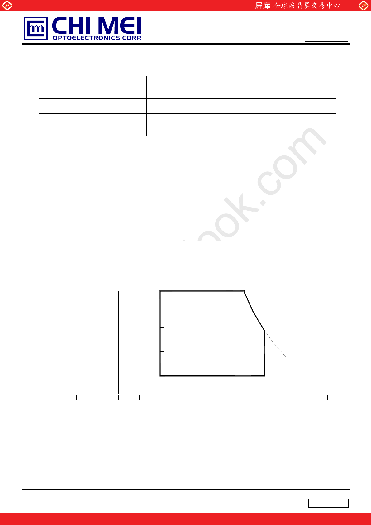
1.5 MECHANICAL SPECIFICATIONS
Item Min. Typ. Max. Unit Note
Horizontal(H) 358.0 358.5 359.0 mm
Module Size
I/F connector mounting
Note (1) Please refer to the attached drawings for more information of front and back outline dimensions.
Vertical(V) 296.0 296.5 297.0 mm
Depth(D) - 17.0 17.5 mm
Weight - 1995 TBD g -
position
The mounting inclination of the connector makes
the screen center within ±0.5mm as the horizontal.
(2)
(1)
(1)
(2) Connector mounting position
+/- 0.5mm
4 / 25
The information described in this specification is tentative and it is possible to be changed without prior notice.
Please contact CMO ’s representative while your product design is based on this specification.
One step solution for LCD / PDP / OLED panel application: Datasheet, inventory and accessory!
Version 0.0
www.panelook.com
Page 5
Global LCD Panel Exchange Center
2. ABSOLUTE MAXIMUM RATINGS
2.1 ABSOLUTE RATINGS OF ENVIRONMENT
Item Symbol
Storage Temperature TST -20 +60 ºC (1)
Operating Ambient Temperature TOP 0 +50 ºC (1), (2)
Shock (Non-Operating) S
Vibration (Non-Operating) V
LCD Cell Life Time L
Note (1) Temperature and relative humidity range is shown in the figure below.
(a) 90 %RH Max. (Ta Љ 40 ºC).
(b) Wet-bulb temperature should be 39 ºC Max. (Ta > 40 ºC).
(c) No condensation.
Note (2) The temperature of panel surface should be 0 ºC Min. and 60 ºC Max.
www.panelook.com
Issued Date: Jan. 08, 2003
Model No.: M170E5 -L02
Tentative
Value
Min. Max.
- 50 G (3), (5)
NOP
- 1.5 G (4), (5)
NOP
50,000 - Hrs
CELL
Unit Note
MTBF
based
Note (3) 11ms, half-sine wave, 1 time for ± X, ± Y, ± Z.
Note (4) 10 ~ 300 Hz, sweep rate 10 min, 30 min for X,Y,Z axis
Note (5) Upon the Vibration and Shock tests, the fixture used to hold the module must be firm and rigid
enough to prevent the module from twisting or bending by the fixture.
Relative Humidity (%RH)
100
90
80
60
Operating Range
40
20
Storage Range
5
Temperature (ºC)
5 / 25
The information described in this specification is tentative and it is possible to be changed without prior notice.
Please contact CMO ’s representative while your product design is based on this specification.
One step solution for LCD / PDP / OLED panel application: Datasheet, inventory and accessory!
8060 -20 400 20-40
Version 0.0
www.panelook.com
Page 6
Global LCD Panel Exchange Center
2.2 ELECTRICAL ABSOLUTE RATINGS
2.2.1 TFT LCD MODULE
Item Symbol
Power Supply Voltage Vcc -0.3 +6.0 V
Logic Input Voltage VIN -0.3 4.3 V
2.2.2 BACKLIGHT UNIT
Item Symbol
Lamp Voltage VL - 2.5K V
Lamp Current IL - 7.5 mA
Lamp Frequency FL - 80 KHz
Note (1) Permanent damage might occur if the module is operated at conditions exceeding the maximum
values.
www.panelook.com
Value
Min. Max.
Value
Min. Max.
Unit Note
Unit Note
Issued Date: Jan. 08, 2003
Model No.: M170E5 -L02
Tentative
(1)
(1), (2), IL = 6.5 mA
RMS
RMS
(1), (2)
Note (2) Specified values are for lamp (Refer to 3.2 for further information).
6 / 25
The information described in this specification is tentative and it is possible to be changed without prior notice.
Please contact CMO ’s representative while your product design is based on this specification.
One step solution for LCD / PDP / OLED panel application: Datasheet, inventory and accessory!
Version 0.0
www.panelook.com
Page 7
Global LCD Panel Exchange Center
www.panelook.com
Issued Date: Jan. 08, 2003
Model No.: M170E5 -L02
3. ELECTRICAL CHARACTERISTICS
3.1 TFT LCD MODULE Ta = 25 ± 2 ºC
Parameter Symbol
Min. Typ. Max.
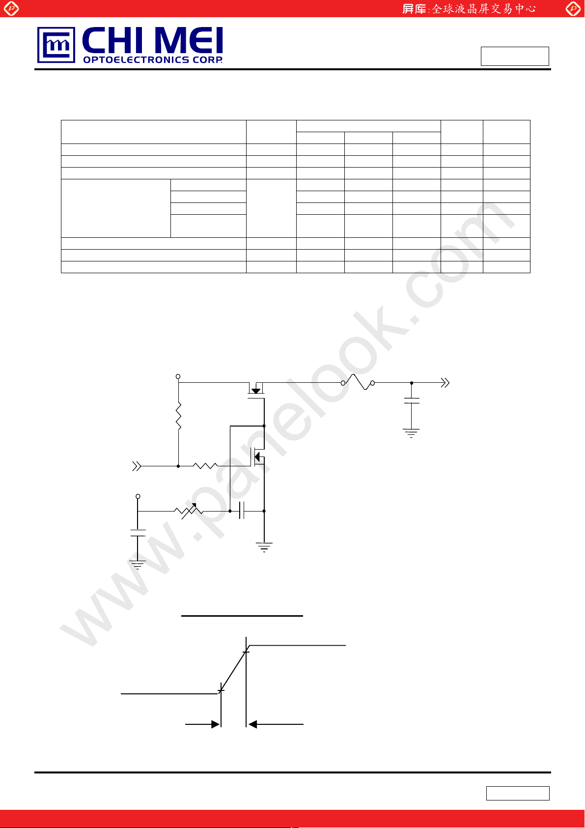
Power Supply Voltage Vcc 4.5 5.0 5.5 V Ripple Voltage VRP - -- 100 mV Rush Current I
- -- TBD A (2)
RUSH
White - 420 TBD mA (3)a
Black - 570 TBD mA (3)b
Power Supply Current
Vertical Stripe - 520 TBD mA (3)c
f
= 75Hz,
V
Vcc=4.5V
lcc
- - TBD mA
LVDS differential input voltage Vid -100 - +100 mV
LVDS common input voltage Vic -- 1.2 -- V
Logic “L” input voltage (SELLVDS) Vil Vss - 0.8 V
Note (1) The module is recommended to operate within specification ranges listed above for normal
Value
Unit Note
Tentative
function.
Note (2) Measurement Conditions:
+5.0V
R1
47K
(High to Low)
(Control Signal)
SW
+12V
C1
1uF
VR1
R2
1K
47K
Q1 2SK1475
C2
0.01uF
Q2
2SK1470
FUSE
C3
1uF
Vcc
(LCD Module Input)
Vcc rising time is 470Ps
+5.0V
0.9Vcc
0.1Vcc
GND
470Ps
7 / 25
The information described in this specification is tentative and it is possible to be changed without prior notice.
Please contact CMO ’s representative while your product design is based on this specification.
One step solution for LCD / PDP / OLED panel application: Datasheet, inventory and accessory!
Version 0.0
www.panelook.com
Page 8
Global LCD Panel Exchange Center
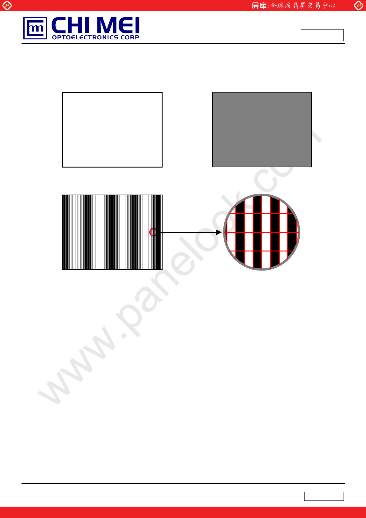
Note (3) The specified power supply current is under the conditions at Vcc = 5.0 V, Ta = 25 ± 2 ºC, fv = 60
Hz, whereas a power dissipation check pattern below is displayed.
www.panelook.com
Issued Date: Jan. 08, 2003
Model No.: M170E5 -L02
Tentative
a. White Pattern
Active Area
c. Vertical Stripe Pattern
b. Black Pattern
Active Area
R
G
R
B
G
R
B
G
R R
G
B
B
B
B
R
R
R
G
G
G
G
B
B
B
B
R
R
Active Area
8 / 25
The information described in this specification is tentative and it is possible to be changed without prior notice.
Please contact CMO ’s representative while your product design is based on this specification.
One step solution for LCD / PDP / OLED panel application: Datasheet, inventory and accessory!
Version 0.0
www.panelook.com
Page 9

Global LCD Panel Exchange Center
3.2 BACKLIGHT UNIT
Parameter Symbol
Lamp Input Voltage VL 585 650 715 V
Lamp Current IL 2.0 6.5 TBD mA
Lamp Turn On Voltage VS
Operating Frequency FL 45 50 80 KHz (3)
Lamp Life Time LBL 40,000 50,000 - Hrs (5)
Power Consumption PL - 16.9 - W (4), IL = 6.5 mA
Note (1) Lamp current is measured by utilizing high-frequency current meters as shown below:
LCD
Module
HV (Pink)
LV (White)
HV (Blue)
LV (Black)
www.panelook.com
Model No.: M170E5 -L02
Value
Min. Typ. Max.
- - 1260(25
- - 1500 (0
o
o
C) V
Unit Note
RMS
C) V
RMS
RMS
1
2
A
Inverter
1
2
A
Issued Date: Jan. 08, 2003
Tentative
I
RMS
(2)
(2)
= 6.5 mA
L
(1)
A
Current Meter
YOKOGAWA 2016
Ta = 2 5 ± 2 ºC
Note (2) The voltage shown above should be applied to the lamp for more than 1 second after startup.
Otherwise, the lamp may not be turned on normally.
Note (3) The lamp frequency may produce interference with horizontal synchronization frequency from the
display, which might cause line flow on the display. In order to avoid interference, the lamp
frequency should be detached from the horizontal synchronization frequency and its harmonics
as far as possible.
Note (4) P
Note (5) The lifetime of lamp can be defined as the time in which it continues to operate under the
Note (6) The waveform of the voltage output of inverter must be area-symmetric and the design of the
= IL VL
L
condition Ta = 25 2
o
C and IL = (2.0) ~ (6.5) mArms until one of the following events occurs:
(a) When the brightness becomes or lower than 50% of its original value.
(b) When the effective ignition length becomes or lower than 80% of its original value. (Effective
ignition length is defined as an area that has less than 70% brightness compared to the
brightness in the center point.)
inverter must have specifications for the modularized lamp. The performance of the Backlight,
such as lifetime or brightness, is greatly influenced by the characteristics of the DC-AC inverter
for the lamp. All the parameters of an inverter should be carefully designed to avoid producing too
much current leakage from high voltage output of the inverter. When designing or ordering the
inverter please make sure that a poor lighting caused by the mismatch of the Backlight and the
inverter (miss-lighting, flicker, etc.) never occurs. If the above situation is confirmed, the module
should be operated in the same manners when it is installed in your instrument.
9 / 25
The information described in this specification is tentative and it is possible to be changed without prior notice.
Please contact CMO ’s representative while your product design is based on this specification.
One step solution for LCD / PDP / OLED panel application: Datasheet, inventory and accessory!
Version 0.0
www.panelook.com
Page 10

Global LCD Panel Exchange Center
The output of the inverter must have symmetrical (negative and positive) voltage waveform and
symmetrical current waveform.(Unsymmetrical ratio is less than 10%) Please do not use the inverter
which has unsymmetrical voltage and unsymmetrical current and spike wave. Lamp frequency may
produce interface with horizontal synchronous frequency and as a result this may cause beat on the
display. Therefore lamp frequency shall be as away possible from the horizontal synchronous
frequency and from its harmonics in order to prevent interference.
Requirements for a system inverter design, which is intended to have a better display performance, a
better power efficiency and a more reliable lamp. It shall help increase the lamp lifetime and reduce its
leakage current.
a. The asymmetry rate of the inverter waveform should be 10% below;
b. The distortion rate of the waveform should be within Ѕ2 ± 10%;
www.panelook.com
Issued Date: Jan. 08, 2003
Model No.: M170E5 -L02
Tentative
c. The ideal sine wave form shall be symmetric in positive and negative polarities.
* Asymmetry rate:
I p
-p
I
| I
* Distortion rate
I
– I –p | / I
p
(or I –p) / I
p
rms
rms
* 100%
10 / 25
The information described in this specification is tentative and it is possible to be changed without prior notice.
Please contact CMO ’s representative while your product design is based on this specification.
One step solution for LCD / PDP / OLED panel application: Datasheet, inventory and accessory!
Version 0.0
www.panelook.com
Page 11

Global LCD Panel Exchange Center
4. BLOCK DIAGRAM
4.1 TFT LCD MODULE
RXO0(+/-)
RXO1(+/-)
RXO2(+/-)
RXO3(+/-)
RXOC(+/-)
RXE0(+/-)
RXE1(+/-)
RXE2(+/-)
RXE3(+/-)
RXEC(+/-)
SELLVDS
Vcc
GND
(JAE-FI-XB30SR-HF11)
INPUT CONNECTOR
VL
LAMP CONNECTOR
(JST-BHSR-02VS-1)
www.panelook.com
LVDS INPUT /
TIMING CONTROLLER
DC/DC CONVERTER &
REFERENCE VOLTAGE
Issued Date: Jan. 08, 2003
Model No.: M170E5 -L02
Tentative
SCAN DRIVER IC
TFT LCD PANEL
(1280x3x1024)
DATA DRIVER IC
BACKLIGHT UNIT
4.2 BACKLIGHT UNIT
1 HV(Pink)
2 LV(White)
1 HV(Blue)
2 LV(Black)
1 HV(Pink)
2 LV(White)
1 HV(Blue)
2 LV(Black)
11 / 25
The information described in this specification is tentative and it is possible to be changed without prior notice.
Please contact CMO ’s representative while your product design is based on this specification.
One step solution for LCD / PDP / OLED panel application: Datasheet, inventory and accessory!
Version 0.0
www.panelook.com
Page 12

Global LCD Panel Exchange Center
5. INPUT TERMINAL PIN ASSIGNMENT
5.1 TFT LCD MODULE
Pin Name Description
1 RXO0- Negative LVDS differential data input. Channel O0 (odd)
2 RXO0+ Positive LVDS differential data input. Channel O0 (odd)
3 RXO1- Negative LVDS differential data input. Channel O1 (odd)
4 RXO1+ Positive LVDS differential data input. Channel O1 (odd)
5 RXO2- Negative LVDS differential data input. Channel O2 (odd)
6 RXO2+ Positive LVDS differential data input. Channel O2 (odd)
7 GND Ground
8 RXOC- Negative LVDS differential clock input. (odd)
9 RXOC+ Positive LVDS differential clock input. (odd)
10 RXO3- Negative LVDS differential data input. Channel O3(odd)
11 RXO3+ Positive LVDS differential data input. Channel O3 (odd)
12 RXE0- Negative LVDS differential data input. Channel E0 (even)
13 RXE0+ Positive LVDS differential data input. Channel E0 (even)
14 GND Ground
15 RXE1- Negative LVDS differential data input. Channel E1 (even)
16 RXE1+ Positive LVDS differential data input. Channel E1 (even)
17 GND Ground
18 RXE2- Negative LVDS differential data input. Channel E2 (even)
19 RXE2+ Positive LVDS differential data input. Channel E2 (even)
20 RXEC- Negative LVDS differential clock input. (even)
21 RXEC+ Positive LVDS differential clock input. (even)
22 RXE3- Negative LVDS differential data input. Channel E3 (even)
23 RXE3+ Positive LVDS differential data input. Channel E3 (even)
24 GND Ground
25 TEST Test pin should be tied to ground.
26 NC Not connection.
27 SELLVDS SELLVDS pin should be tied to ground or open.
28 VCC +5.0V power supply
29 VCC +5.0V power supply
30 VCC +5.0V power supply
Note (1) Connector Part No.: FI-XB30SR-HF11 or equivalent
www.panelook.com
Issued Date: Jan. 08, 2003
Model No.: M170E5 -L02
Tentative
Note (2) The first pixel is odd.
Note (3) Input signal of even and odd clock should be the same timing.
12 / 25
The information described in this specification is tentative and it is possible to be changed without prior notice.
Please contact CMO ’s representative while your product design is based on this specification.
Version 0.0
One step solution for LCD / PDP / OLED panel application: Datasheet, inventory and accessory!
www.panelook.com
Page 13

Global LCD Panel Exchange Center
SELLVDS = Low or Open
LVDS Channel E0
LVDS Channel E1
LVDS Channel E2
LVDS Channel E3
LVDS Channel O0
LVDS Channel O1
LVDS Channel O2
LVDS Channel O3
LVDS output D7 D6 D4 D3 D2 D1 D0
Data order EG0 ER5 ER4 ER3 ER2 ER1 ER0
LVDS output D18 D15 D14 D13 D12 D9 D8
Data order EB1 EB0 EG5 EG4 EG3 EG2 EG1
LVDS output D26 D25 D24 D22 D21 D20 D19
Data order DE NA NA EB5 EB4 EB3 EB2
LVDS output D23 D17 D16 D11 D10 D5 D27
Data order NA EB7 EB6 EG7 EG6 ER7 ER6
LVDS output D7 D6 D4 D3 D2 D1 D0
Data order OG0 OR5 OR4 OR3 OR2 OR1 OR0
LVDS output D18 D15 D14 D13 D12 D9 D8
Data order OB1 OB0 OG5 OG4 OG3 OG2 OG1
LVDS output D26 D25 D24 D22 D21 D20 D19
Data order DE NA NA OB5 OB4 OB3 OB2
LVDS output D23 D17 D16 D11 D10 D5 D27
Data order NA OB7 OB6 OG7 OG6 OR7 OR6
www.panelook.com
Issued Date: Jan. 08, 2003
Model No.: M170E5 -L02
Tentative
13 / 25
The information described in this specification is tentative and it is possible to be changed without prior notice.
Please contact CMO ’s representative while your product design is based on this specification.
One step solution for LCD / PDP / OLED panel application: Datasheet, inventory and accessory!
Version 0.0
www.panelook.com
Page 14

Global LCD Panel Exchange Center
5.2 BACKLIGHT UNIT
Pin Symbol Description Remark
1 HV High Voltage Pink
2 LV Low Voltage White
1 HV High Voltage Blue
2 LV Low Voltage Black
Note (1) Connector Part No.: JST-BHSR-02VS-1 or equivalent
Note (2) User’s connector Part No.: JST-SM02B-BHSS-1-TB (JST) or equivalent
5.3 COLOR DATA INPUT ASSIGNMENT
The brightness of each primary color (red, green and blue) is based on the 8-bit gray scale data input for
the color. The higher the binary input, the brighter the color. The table below provides the assignment of
color versus data input.
Color
R7 R6 R5 R4 R3 R2 R1 R0 G7 G6 G5 G4 G3 G2 G1 G0 B7 B6 B5 B4 B3 B2 B1 B0
Basic
Colors
Gray
Scale
Of
Red
Black
Red
Green
Blue
Cyan
Magenta
Ye ll ow
White
Red(0) / Dark
Red(1)
Red(2)
:
:
Red(253)
Red(254)
Red(255)
0
0
1
1
0
0
0
0
0
0
1
1
1
1
1
1
0
0
0
0
0
0
:
:
:
:
1
1
1
1
1
1
www.panelook.com
Issued Date: Jan. 08, 2003
Model No.: M170E5 -L02
Tentative
Data Signal
Red Green Blue
0
0
0
0
0
0
0
0
0
0
0
0
0
0
0
0
0
0
0
0
0
0
1
1
1
1
1
1
0
0
0
0
0
0
0
0
0
0
0
0
0
0
0
0
0
0
0
0
0
0
1
1
1
1
1
1
1
1
0
0
0
0
0
0
0
0
0
0
0
0
0
0
0
0
0
0
0
0
0
0
1
1
1
1
1
1
1
1
0
0
0
0
0
0
1
1
1
1
1
1
1
1
1
1
1
1
1
1
1
1
1
1
1
1
1
1
0
0
0
0
0
0
0
0
1
1
1
1
1
1
1
1
1
1
1
1
1
1
1
1
1
1
1
1
1
1
0
0
0
0
0
0
0
0
1
1
1
1
1
1
1
1
1
1
1
1
1
1
1
1
1
1
1
1
1
1
0
0
0
0
0
0
0
0
0
0
0
0
0
0
0
0
0
0
0
0
0
0
0
0
0
0
0
1
0
0
0
0
0
0
0
0
0
0
0
0
0
0
0
0
0
0
0
0
1
0
0
0
0
0
0
0
0
0
0
0
0
0
0
0
0
0
:
:
:
:
:
:
:
:
:
:
:
:
:
:
:
:
:
:
:
:
:
:
:
:
:
:
:
:
:
:
:
:
:
:
:
:
:
:
:
:
:
:
:
:
1
1
1
1
0
1
0
0
0
0
0
0
0
0
0
0
0
0
0
0
0
0
1
1
1
1
1
0
0
0
0
0
0
0
0
0
0
0
0
0
0
0
0
0
1
1
1
1
1
1
0
0
0
0
0
0
0
0
0
0
0
0
0
0
0
0
Green(0) / Dark
Gray
Scale
Of
Green
Gray
Scale
Of
Blue
Note (1) 0: Low Level Voltage, 1: High Level Voltage
Green(1)
Green(2)
:
:
Green(253)
Green(254)
Green(255)
Blue(0) / Dark
Blue(1)
Blue(2)
:
:
Blue(253)
Blue(254)
Blue(255)
0
0
0
0
0
0
0
0
0
0
0
0
0
0
0
0
0
0
0
0
0
0
0
0
0
0
0
0
0
0
0
0
0
0
0
0
0
0
0
1
0
0
0
0
0
0
0
0
0
0
0
0
0
0
0
0
0
0
0
0
0
0
1
0
0
0
0
0
0
0
0
0
:
:
:
:
:
:
:
:
:
:
:
:
:
:
:
:
:
:
:
:
:
:
:
:
:
:
:
:
:
:
:
:
:
:
:
:
:
:
:
:
:
:
:
:
:
:
:
:
0
0
0
0
0
0
0
0
1
1
1
1
1
1
0
1
0
0
0
0
0
0
0
0
0
0
0
0
0
0
0
0
1
1
1
1
1
1
1
0
0
0
0
0
0
0
0
0
0
0
0
0
0
0
0
0
1
1
1
1
1
1
1
1
0
0
0
0
0
0
0
0
0
0
0
0
0
0
0
0
0
0
0
0
0
0
0
0
0
0
0
0
0
0
0
0
0
0
0
0
0
0
0
0
0
0
0
0
0
0
0
0
0
0
0
0
0
0
0
1
0
0
0
0
0
0
0
0
0
0
0
0
0
0
0
0
0
0
0
0
0
0
1
0
:
:
:
:
:
:
:
:
:
:
:
:
:
:
:
:
:
:
:
:
:
:
:
:
:
:
:
:
:
:
:
:
:
:
:
:
:
:
:
:
:
:
:
:
:
:
:
:
0
0
0
0
0
0
0
0
0
0
0
0
0
0
0
0
1
1
1
1
1
1
0
1
0
0
0
0
0
0
0
0
0
0
0
0
0
0
0
0
1
1
1
1
1
1
1
0
0
0
0
0
0
0
0
0
0
0
0
0
0
0
0
0
1
1
1
1
1
1
1
1
14 / 25
The information described in this specification is tentative and it is possible to be changed without prior notice.
Please contact CMO ’s representative while your product design is based on this specification.
Version 0.0
One step solution for LCD / PDP / OLED panel application: Datasheet, inventory and accessory!
www.panelook.com
Page 15

Global LCD Panel Exchange Center
6. INTERFACE TIMING
6.1 INPUT SIGNAL TIMING SPECIFICATIONS
The input signal timing specifications are shown as the following table and timing diagram.
Signal Item Symbol Min. Typ. Max. Unit Note
Frequency Fc - 54 67.5 MHz -
LVDS Clo c k
LVDS Data
Vertical Active Display Term
Horizontal Active Display Term
NoteΚ(1) Because this module is operated by DE only mode, Hsync and Vsync input signals should be
Period Tc 14.8 18.5 - ns
High Time Tch - 4/7 - Tc Low Time Tcl - 3/7 - Tc Setup Time Tlvs 600 - - ps Hold Time Tlvh 600 - - ps Frame Rate Fr 56 60 75 Hz Tv=Tvd+Tvb
Total Tv 1034 1066 1274 Th Display Tvd 1024 1024 1024 Th Blank Tvb Tv-Tvd 42 Tv-Tvd Th Total Th TBD 844 TBD Tc Th=Thd+Thb
Display Thd 640 640 640 Tc Blank Thb Th-Thd 204 Th-Thd Tc -
www.panelook.com
Issued Date: Jan. 08, 2003
Model No.: M170E5 -L02
Tentative
set to low logic level or ground. Otherwise, this module would operate abnormally.
(2) The relationship between Fc and Th must comply with the (Th-216)/Fc>9.3 criterion.
INPUT SIGNAL TIMING DIAGRAM
15 / 25
The information described in this specification is tentative and it is possible to be changed without prior notice.
Please contact CMO ’s representative while your product design is based on this specification.
One step solution for LCD / PDP / OLED panel application: Datasheet, inventory and accessory!
Version 0.0
www.panelook.com
Page 16

Global LCD Panel Exchange Center
www.panelook.com
Issued Date: Jan. 08, 2003
Model No.: M170E5 -L02
Tentative
6.2 POWER ON/OFF SEQUENCE
To prevent a latch-up or DC operation of LCD module, the power on/off sequence should follow the
conditions shown in the following diagram.
Note.
(1) The supply voltage of the external system for the module input should be the same as the definition of Vcc.
(2) Please apply the lamp voltage within the LCD operation range. When the backlight turns on before the LCD
operation of the LCD turns off, the display may, instantly, function abnormally.
(3) In case of
(4) T4 should be measured after the module has been fully discharged between power on/off periods.
(5) Interface signal shall not be kept at high impedance when the power is on.
VCC = off level, please keep the level of input signals on the low or keep a high impedance.
16 / 25
The information described in this specification is tentative and it is possible to be changed without prior notice.
Please contact CMO ’s representative while your product design is based on this specification.
Version 0.0
One step solution for LCD / PDP / OLED panel application: Datasheet, inventory and accessory!
www.panelook.com
Page 17

Global LCD Panel Exchange Center
7. OPTICAL CHARACTERISTICS
7.1 TEST CONDITIONS
Item Symbol Value Unit
Ambient Temperature Ta
Ambient Humidity Ha
Supply Voltage VCC 5.0 V
Input Signal According to typical value in "3. ELECTRICAL CHARACTERISTICS"
Inverter Current IL (6.5) mA
Inverter Driving Frequency FL 50 KHz
Inverter
7.2 OPTICAL SPECIFICATIONS
The relative measurement methods of optical characteristics are shown in 7.2. The following items should
be measured under the test conditions described in 7.1 and stable environment shown in Note (6).
Item Symbol Condition Min. Typ. Max. Unit Note
Contrast Ratio CR (300) (400) - - (2), (6)
Response Time
Center Luminance of White L
White Variation
Cross Talk CT - - (5.0) % (5), (6)
Red
Color
Chromaticity
Viewing Angle
TCO’99 Luminance
Uniformity
(Angular-dependent)
TCO’99 Luminance Contrast
(Angular-dependent)
Green
Blue
White
Horizontal
Ver t ical
www.panelook.com
Issued Date: Jan. 08, 2003
Model No.: M170E5 -L02
Tentative
o
25r2
50r10
TR - (5) TBD ms
- (11) TBD ms
T
F
C
GW
=0q, TY =0q
T
Rx (0.649) Ry (0.350) -
Gx (0.297) -
x
Viewing Normal Angle
Gy (0.600) Bx (0.140) -
(250) (300) - cd/m2(4), (6)
- (1.25) (1.40) - (6), (7)
Typ
- 0.03
Typ
+ 0.03
By (0.070) Wx
Wy
Tx+
T
x
TY+
T
Y
L
R
C
m
(60) (70) -
CRt10
-
ˀʳ
ˀʳ
(60) (70) (50) (60) (50) (60) -
(0.313)
(0.329)
- - 1.7 - (8)
0.5 - - - (9)
C
%RH
(3)
(1), (6)
-
-
Deg. (1), (6)
17 / 25
The information described in this specification is tentative and it is possible to be changed without prior notice.
Please contact CMO ’s representative while your product design is based on this specification.
One step solution for LCD / PDP / OLED panel application: Datasheet, inventory and accessory!
Version 0.0
www.panelook.com
Page 18

Global LCD Panel Exchange Center
T
Note (1) Definition of Viewing Angle (Tx, Ty):
www.panelook.com
Issued Date: Jan. 08, 2003
Model No.: M170E5 -L02
Tentative
TX- = 90º
x-
6 o’clock
T
y- = 90º
y-
Note (2) Definition of Contrast Ratio (CR):
The contrast ratio can be calculated by the following expression.
Normal
Tx = Ty = 0º
Ty- Ty
Tx
Tx
12 o’clock direction
y+
T
y+ = 90º
x+
TX+ = 90º
Contrast Ratio (CR) = L255 / L0
L255: Luminance of gray level 255
L 0: Luminance of gray level 0
CR = CR (5)
CR (X) is corresponding to the Contrast Ratio of the point X at Figure in Note (7).
Note (3) Definition of Response Time (T
100%
90%
Optical
Response
Gray Level 255
10%
0%
, TF):
R
Gray Level 0
T
R T
Gray Level 255
ime
F
18 / 25
The information described in this specification is tentative and it is possible to be changed without prior notice.
Please contact CMO ’s representative while your product design is based on this specification.
One step solution for LCD / PDP / OLED panel application: Datasheet, inventory and accessory!
Version 0.0
www.panelook.com
Page 19

Global LCD Panel Exchange Center
A
(
)
A
(
)
(
)
Note (4) Definition of Luminance of White (LC):
Measure the luminance of gray level 255 at center point
L
= L (5)
C
L (x) is corresponding to the luminance of the point X at Figure in Note (7).
Note (5) Definition of Cross Talk (CT):
www.panelook.com
Issued Date: Jan. 08, 2003
Model No.: M170E5 -L02
Tentative
CT = | Y
Where:
Y
= Luminance of measured location without gray level 0 pattern (cd/m2)
A
Y
= Luminance of measured location with gray level 0 pattern (cd/m2)
B
(0, 0)
Y
(D/8,W/2)
A, L
Y
(D/2,7W/8)
A, D
Note (6) Measurement Setup:
The LCD module should be stabilized at given temperature for 20 minutes to avoid abrupt
temperature change during measuring. In order to stabilize the luminance, the measurement
– YA | / YA u 100 (%)
B
ctive Area
Gray 128
Y
Y
D,W
A, U
A, R
(D/2,W/8)
(7D/8,W/2)
(D/4,W/4)
Y
(D/8,W/2)
B, L
Y
(D/2,7W/8)
B, D
0, 0
ctive Area
Gray 0
Gray 128
Y
(D/2,W/8)
B, U
Y
(7D/8,W/2)
B, R
(3D/4,3W/4)
D,W
should be executed after lighting Backlight for 20 minutes in a windless room.
LCD Module
LCD Panel
Center of the Screen
Photometer
(TOPCON BM-5A)
Field of View = 2º
500 mm
Light Shield Room
(Ambient Luminance < 2 lux)
19 / 25
The information described in this specification is tentative and it is possible to be changed without prior notice.
Please contact CMO ’s representative while your product design is based on this specification.
Version 0.0
One step solution for LCD / PDP / OLED panel application: Datasheet, inventory and accessory!
www.panelook.com
Page 20

Global LCD Panel Exchange Center
Note (7) Definition of White Variation (GW):
Measure the luminance of gray level 255 at 9 points
www.panelook.com
Issued Date: Jan. 08, 2003
Model No.: M170E5 -L02
Tentative
Maximum [L (1), L (2), L (3), L (4), L (5), L (6), L (7), L (8), L (9)]
GW =
Minimum [L (1), L (2), L (3), L (4), L (5), L (6), L (7), L (8), L (9)]
D/10
Horizontal Line
D
D/2
9D/10
W/10
1
2
3
X
W
W/2
4
5
6
: Test Point
X=1 to 9
Vertical Line
9W/10
7 8 9
Active Area
20 / 25
The information described in this specification is tentative and it is possible to be changed without prior notice.
Please contact CMO ’s representative while your product design is based on this specification.
One step solution for LCD / PDP / OLED panel application: Datasheet, inventory and accessory!
Version 0.0
www.panelook.com
Page 21

Global LCD Panel Exchange Center
W
Note (8) Definition of TCO 99 Luminance Uniformity (Angular-dependent) (LR):
www.panelook.com
Issued Date: Jan. 08, 2003
Model No.: M170E5 -L02
Tentative
D/2
D/2
W/2
W/2
0.1 D
D
0.1 D
Luminance is measured at the center measurement position “C” on the LCD panel. The optical
axis of the luminance meter shall be aligned with the normal of the panel surface. The measuring
distance between the photometer and the surface of the panel is defined as:
Md (cm) = diagonal of the panel (cm) X 1.5 with minimum distance 50 cm.
The panel is rotated around a vertical axis which passes the center of the display by changing
the azimuthal angle to +30q. The distance between the panel and the photometer remains
unchanged and the measured point is exact the same as the previous measured point.
The photometer is then rotated by changing its azimuthal angle with the fixed distance to the
panel. Luminance at points “L” and “R” are given:
LCD panel
30q
R
L
L
min, +30
min, +30
q
q and L
max, +30
q
C
Md
Photometer
L
L
max, +30
The LCD panel is then rotated to another azimuthal angle to -30q; and L
q
min, -3T
q and L
max, -30
q
are obtained by using the same procedure.
The Luminance Uniformity (L
R) is calculated as follow:
R = ((L
L
max, +30
q/ L
min, +30
q)+( L
max, -30
q/ L
min, -30
q)) / 2.
21 / 25
The information described in this specification is tentative and it is possible to be changed without prior notice.
Please contact CMO ’s representative while your product design is based on this specification.
One step solution for LCD / PDP / OLED panel application: Datasheet, inventory and accessory!
Version 0.0
www.panelook.com
Page 22

Global LCD Panel Exchange Center
Note (9) Definition of TCO 99 Luminance Contrast (Angular-dependent) (Cm):
www.panelook.com
Issued Date: Jan. 08, 2003
Model No.: M170E5 -L02
Tentative
W
Luminance contrast is measured at the center point of the LCD panel “C” along with the normal
of the display with the same distance described in Note 13. The display is then rotated around
the vertical axis by changing its azimuthal axis to +30q; and this gives:
D/2
L
255
G.L., +30
D
q and L
D/2
0 G.L., +30
W/2
W/2
q.
The LCD panel is then rotated to azimuthal angle to -30q; and L
are obtained by using the same procedure. The Luminance Contrast (Cm) is calculated:
For both +30q and -30q. The lower value for Cm is reported.
LCD panel
30q
C
Cm = (L
255
G. L .
- L
0 G.L.
)/ (L255
Photometer
+ L
G. L .
0 G. L., -30
)
0 G.L
q and L
255 G.L., -30
q
22 / 25
The information described in this specification is tentative and it is possible to be changed without prior notice.
Please contact CMO ’s representative while your product design is based on this specification.
One step solution for LCD / PDP / OLED panel application: Datasheet, inventory and accessory!
Version 0.0
www.panelook.com
Page 23

Global LCD Panel Exchange Center
www.panelook.com
Issued Date: Jan. 08, 2003
Model No.: M170E5 -L02
Tentative
8. PRECAUTIONS
8.1 ASSEMBLY AND HANDLING PRECAUTIONS
(1) Do not apply rough force such as bending or twisting to the module during assembly.
(2) To assemble or install module into user’s system can be only in clean working areas. The dust and oil
may cause electrical short or worsen the polarizer.
(3) It’s not permitted to have pressure or impulse on the module because the LCD panel and Backlight
will be damaged.
(4) Always follow the correct power sequence when LCD module is connecting and operating. This can
prevent damage to the CMOS LSI chips during latch-up.
(5) Do not pull the I/F connector in or out while the module is operating.
(6) Do not disassemble the module.
(7) Use a soft dry cloth without chemicals for cleaning, because the surface of polarizer is very soft and
easily scratched.
(8) It is dangerous that moisture come into or contacted the LCD module, because moisture may damage
LCD module when it is operating.
(9) High temperature or humidity may reduce the performance of module. Please store LCD module
within the specified storage conditions.
(10) When ambient temperature is lower than 10ºC may reduce the display quality. For example, the
response time will become slowly, and the starting voltage of CCFL will be higher than room
temperature.
8.2 SAFETY PRECAUTIONS
(1) The startup voltage of Backlight is approximately 1000 Volts. It may cause electrical shock while
assembling with inverter. Do not disassemble the module or insert anything into the Backlight unit.
(2) If the liquid crystal material leaks from the panel, it should be kept away from the eyes or mouth. In
case of contact with hands, skin or clothes, it has to be washed away thoroughly with soap.
(3) After the module’s end of life, it is not harmful in case of normal operation and storage.
23 / 25
The information described in this specification is tentative and it is possible to be changed without prior notice.
Please contact CMO ’s representative while your product design is based on this specification.
One step solution for LCD / PDP / OLED panel application: Datasheet, inventory and accessory!
Version 0.0
www.panelook.com
Page 24

Global LCD Panel Exchange Center
www.panelook.com
5
One step solution for LCD / PDP / OLED panel application: Datasheet, inventory and accessory!
www.panelook.com
Page 25

Global LCD Panel Exchange Center
www.panelook.com
E207943
One step solution for LCD / PDP / OLED panel application: Datasheet, inventory and accessory!
www.panelook.com
 Loading...