

Page 1
Global LCD Panel Exchange Center
www.panelook.com
One step solution for LCD / PDP / OLED panel application: Datasheet, inventory and accessory!
www.panelook.com
Page 2
Global LCD Panel Exchange Center
CONTENTS
REVISION HISTORY
GENERAL DESCRIPTION
1. ABSOLUTE MAXIMUM RATINGS
1.1 ABSOLUTE RATINGS OF ENVIRONMENT
1.2 ELECTRICAL ABSOLUTE RATINGS
2. ELECTRICAL SPECIFICATIONS
2.1 TFT LCD MODULE
2.2 BACKLIGHT UNIT
www.panelook.com
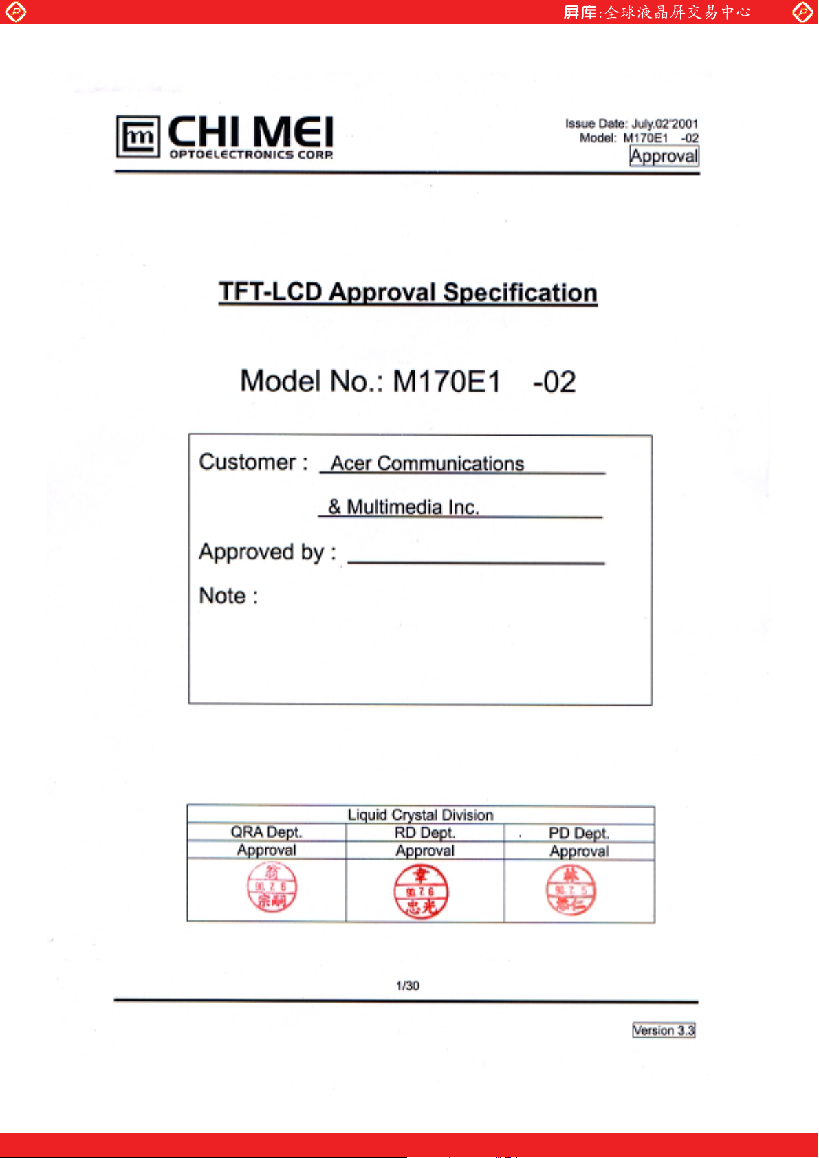
Issue Date: July.02’2001
Model: M170E1 -02
Approval
3. BLOCK DIAGRAM
3.1 TFT LCD MODULE
3.2 BACKLIGHT UNIT
4. INTERFACE SPECIFICATIONS
4.1 THE LVDS INTERFACE SIGNAL DESCRIPTION
4.2 IINPUT SIGNAL TIMING
4.3 COLOR DATA INPUT ASSIGNMENT
5. OPTICAL CHARACTERISTICS
5.1 TEST CONDITIONS
5.2 OPTICAL SPECIFICATIONS
6. OUTLINE DIMENTION
7. PRECAUTION
7.1 ASSEMBLY AND HANDLING PRECAUTION
7.2 SAFETY PRECAUTION
8. 8. PACKAGING
8.1 PACKING SPECIFICATIONS
8.2 PACKING Method
2/30
Version 3.3
One step solution for LCD / PDP / OLED panel application: Datasheet, inventory and accessory!
www.panelook.com
Page 3

Global LCD Panel Exchange Center
9. INCOMING INSPECTION DA
10. DEFINITION OF SHIPPING LABEL ON MODULE
www.panelook.com
Issue Date: July.02’2001
Model: M170E1 -02
Approval
3/30
Version 3.3
One step solution for LCD / PDP / OLED panel application: Datasheet, inventory and accessory!
www.panelook.com
Page 4
Global LCD Panel Exchange Center
Version Date Description
Ver 3 .0
Ver 3 .1
Ver 3 .2
Ver 3 .3
May.31,’01
Jun.14 ,’01
Jun.19,’01
July.02’01
Issue Approval Specification
Page 5
Update Depth of Module Size: 21(Max.)15(Max.)/ Add Note(1)
Page 7
Update VSA of 2.1 TFT LCD MODULE POWER CONSUMPTION: Typ: 1310
Page 9
Update 3.1 TFT LCD MODULE.
Page 10~14
Update Interface Signal CXA1: Pin10, 11, 12, 42, 43, 44
Update Interface Signal CXA2: Pin 30, 32, 35
Update Interface Signal CXB1: Pin 10, 11 ,12, 42, 44, 45
Update Interface Signal CXB2: Pin 2, 3, 4, 30, 32, 35
Update Interface Signal CNY1: Pin 1, 2, 9, 13, 18, 19, 20
Page 15
Delete Start Pulse Signal Delay Time & Driver Output Delay Time1 & Time2
Page 16, 19
Update Timing Chart
Page 18
Delete Output Delay Time(1)
Page 21
Update White Variation of 5.2 OPTICAL SPECIFICATIONS:
1.25(Typ.)/1.4(Max.)20(Typ.)/30(Max.)/ %(Unit)
Page 24
Add Note(8).
Page 5
Update depth of module size: -(Typ.)/15(Max.)13(Typ.)/14(Max.)
Page 20
Add Power Sequence Spec.
Page 22
Update Viewing Angle:θ
Conditions: CRЊ10 CR=5
Page 25
Update Note(8).
Page 20
Update Power Sequence Spec.
Page 25
Update Note(8).
www.panelook.com
Issue Date: July.02’2001
Model: M170E1 -02
Approval
REVISION HISTORY
+:50(Min.)/60(Typ.)70(Min.)/80(Typ.)
x
θ
-:50(Min.)/60(Typ.)70(Min.)/80(Typ.)
x
θ
+:30(Min.)/40(Typ.) 50(Min.)/60(Typ.)
Y
θ
-: 50(Min.)/60(Typ.) 70(Min.)/80(Typ.)
Y
4/30
Version 3.3
One step solution for LCD / PDP / OLED panel application: Datasheet, inventory and accessory!
www.panelook.com
Page 5
Global LCD Panel Exchange Center
GENERAL DESCRIPTION
OVERVIEW
This product is a 17.0” TFT Liquid Crystal Display Module with 2 dual CCFLs Backlight unit and 30 pins
LVDS interface. This module supports 1280 x 1024 SXGA resolution and can display 16 million colors.
The inverter module for Backlight is not built in.
FEATURES
-SXGA (1280x1024 pixels) resolution
-2 dual CCFLs (Cold Cathode Fluorescent Lamp)
-DE only mode
www.panelook.com
Issue Date: July.02’2001
Model: M170E1 -02
Approval
APPLICATION
-TFT-LCD Monitor
GENERAL SPECIFICATI0NS
Item Spec. Unit
Screen Size 17.0 Diagonal inch
Bezel Opening Area 342.0(H) x 274.4(V) mm
Effective Display Area 337.92(H) x 270.34(V) mm
Driver Element a-si TFT active matrix -
Pixel Number 1280 x R.G.B. x 1024 pixel
Pixel Pitch 0.264(H) x 0.264(W) mm
Pixel Arrangement RGB vertical stripe -
Display Colors 16M color
Transmissive NC Normally White -
Surface Treatment Haze 25%,Hard-Coating,Anti-static -
MECHANICAL SPECIFICATIONS
Item Min. Typ. Max. Unit Note
Horizontal(H) 403.5 404 404.5 mm
Module Size
Vertical(V) 321.7 322.2 322.7 mm
Depth(D) - 13 14 mm (1)
Weight - 2,000 2,150
g
Note (1) The Depth is without boss.
5/30
Version 3.3
One step solution for LCD / PDP / OLED panel application: Datasheet, inventory and accessory!
www.panelook.com
Page 6
Global LCD Panel Exchange Center
1. ABSOLUTE MAXIMUM RATINGS
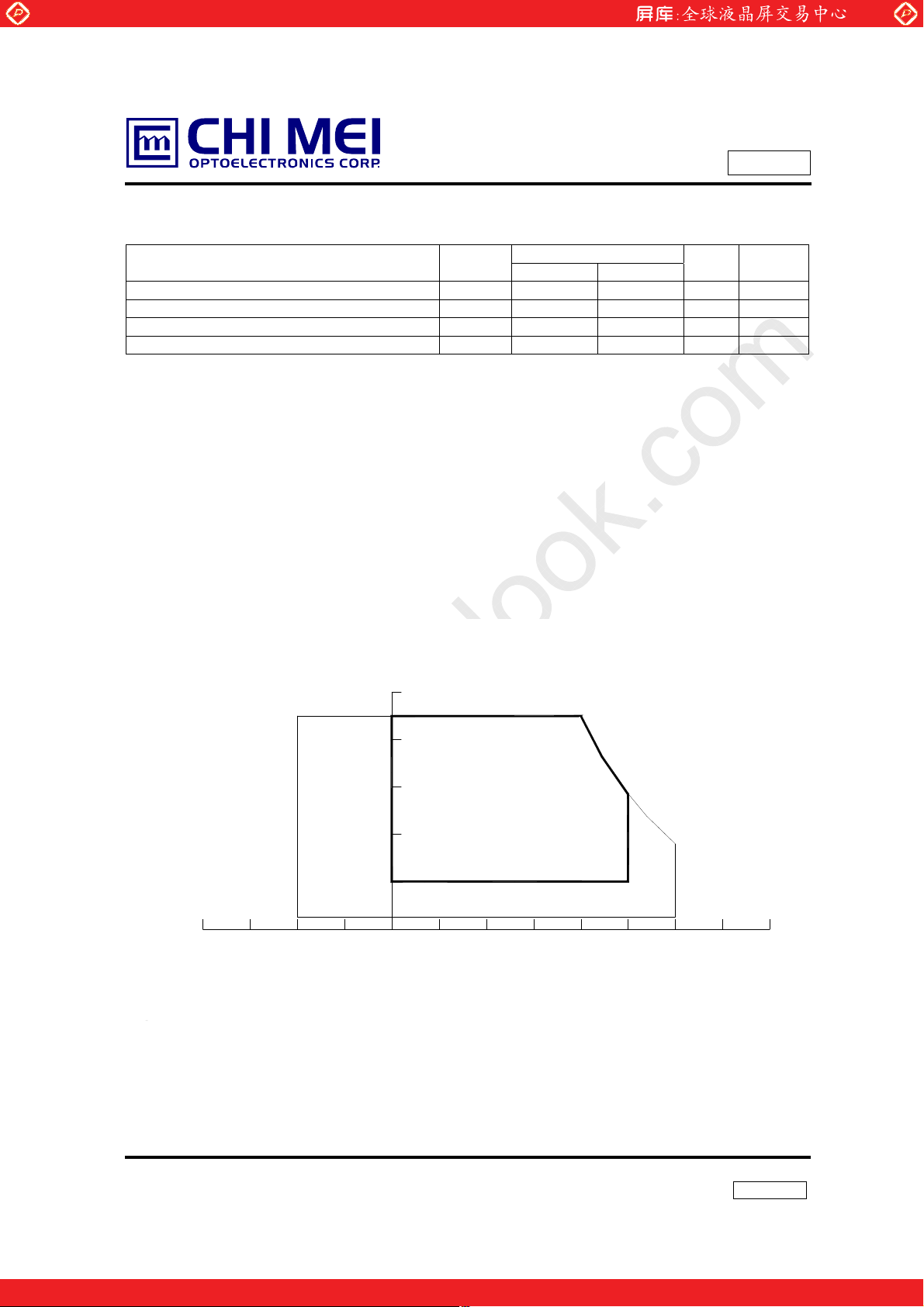
1.1 ABSOLUTE RATINGS OF ENVIRONMENT
Item Symbol
Storage temperature Tst -20 +60 ºC (1)
Operating temperature (Ambient Temperature) Top 0 +50 ºC (1),(2)
Shock(non-operating) Snop - 30 G (3),(5)
Vibration(non-operating) Vnop - 1.5 G (4),(5)
Note (1) Temperature and relative humidity range is shown in the figure below.
(a) 90 %RH Max. (Ta Љ 40 ºC).
(b) Wet-bulb temperature should be 39 ºC Max. (Ta > 40 ºC).
(c) No condensation.
Note (2) The temperature of panel surface should be 0 ºC Min. and 60 ºC Max.
Note (3) 6 ms, half sine wave, 1 time for ± X, ± Y, ± Z.
Note (4) 10 ~ 500 Hz, 0.5 Hr each X, Y, Z.
Note (5) At testing Vibration and Shock, the fixture in holding the module has to be hard and rigid
enough so that the module would not be twisted or bent by the fixture.
www.panelook.com
Min. Max.
Values
Issue Date: July.02’2001
Model: M170E1 -02
Approval
Unit Note
-40
-40
-20
-20
Relative Humidity (%RH)
Relative Humidity (%RH)
100
100
90
90
80
80
60
60
Operating Range
Operating Range
40
40
20
20
Storage Range
5
5
Temperature (ºC)
Temperature (ºC)
Storage Range
0
0
20
20
40
40
60
60
80
80
6/30
Version 3.3
One step solution for LCD / PDP / OLED panel application: Datasheet, inventory and accessory!
www.panelook.com
Page 7
Global LCD Panel Exchange Center
1.2 ELECTRICAL ABSOLUTE RATINGS
(1) TFT LCD MODULE
Item Symbol
Power Supply Voltage Vcc -0.3 6.0 V
Input Signal Voltage VIN -0.3 4.3 V
(2) BACKLIGHT UNIT
Item Symbol
Lamp Current IL 6.0 13.0 14.0 m A
Lamp Frequency FL 30 45 80 KHz (1)
Note (1) Permanent damage to device may occur if maximum values are exceeded. Function operation
should be restricted to the conditions described under Normal Operating Conditions.
Note (2) Specified values are for a dual lamp (Refer to the Note (1) of 2.2 BACKLIGHT UNIT for further
information).
www.panelook.com
Valu es
Min. Max.
Value
Min. Typ. Max.
Issue Date: July.02’2001
Model: M170E1 -02
Approval
Unit Note
Ta = 25 ± 2 ºC
Unit Note
(1),(2)
RMS
2. ELECTRICAL SPECIFICATIONS
2.1 TFT LCD MODULE POWER CONSUMPTION
Synbol
ISA
ISD
IGD
IGH
IGL
IREF
VSA - 10 - V
VSD - 3.3 - V
VGD - 3.3 - V
VGH - 23 - V
VGL - -7 - V
VREF - 9.6 - V
Min Typ Max
73.5
9.72
0.729
3.62
2.26
3.07
Valu e
7/30
Unit
-
-
-
-
-
-
203
19.9
0.731
3.72
2.71
3.07
mA
mA
mA
mA
mA
mA
Version 3.3
One step solution for LCD / PDP / OLED panel application: Datasheet, inventory and accessory!
www.panelook.com
Page 8
Global LCD Panel Exchange Center
2.2 BACKLIGHT UNIT
Parameter Symbol
Lamp Input Voltage VL 640 720 800 V
Lamp Current IL 6.0 13.0 14.0 mA
Lamp Turn On Voltage VS
Operating Frequency FL 30 45 80 KHz (1)
Lamp Life Time LBL 50,000 - - Hrs 13mA
Power Consumption PL - 9360 - MW (4)
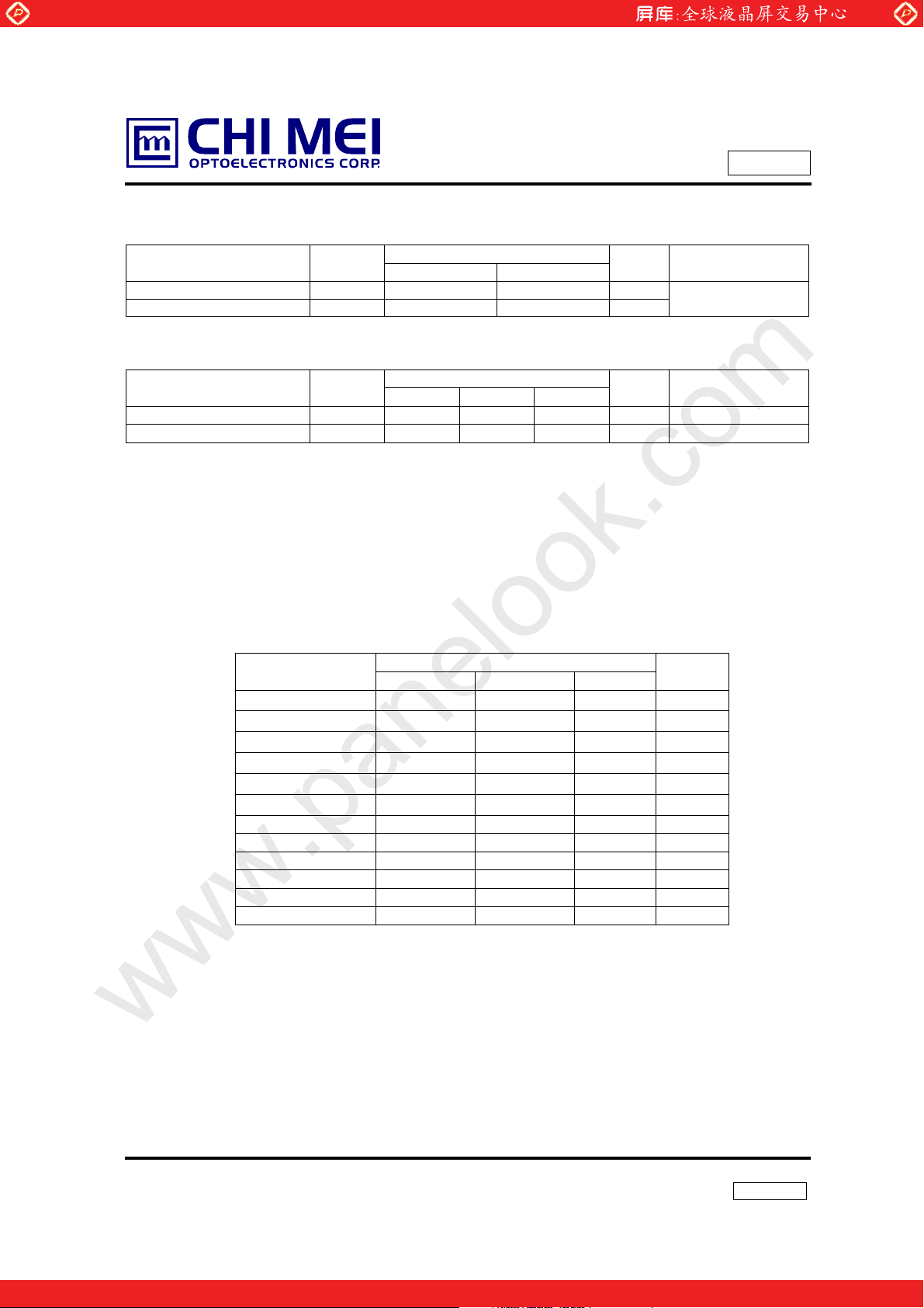
Note (1) Lamp current is measured by utilizing a current meter for high frequency as shown below:
Note (2) The voltage shown above should be applied to the lamp for more than 1 second after startup.
Note (3) The lamp frequency may produce interference with horizontal synchronous frequency from the
Note (4) P
Note (5) The lifetime (Hr) of a lamp can be defined as the time in which it continues to operate under the
Note (6) The waveform of the voltage output of inverter must be area-symmetric and the design of the
LCD
Module
Otherwise the lamp may not be turned on.
display, and this may cause line flow on the display. In order to avoid interference the lamp
frequency should be detached from the horizontal synchronous frequency and its harmonics as
far as possible.
= ILVL.
L
condition Ta = 252к and I
(a) When the brightness becomes 50% or lower than its original,
(b) When the effective ignition length becomes 80% or lowers than its original value. (Effective
ignition length is defined as an area that has less than 70% brightness compared to the
brightness in the center point.)
inverter must have specifications for the modularized lamp. The performance of the backlight,
such as lifetime or brightness, is greatly influenced by the characteristics of the DC-AC inverter
for the lamp. All the parameters of an inverter should be designed with care so as not to produce
too much current leakage from high-voltage output of the inverter. When designing or ordering
the inverter please make sure that a poor lighting caused by the mismatch of the backlight and
the inverter (miss-lighting, flicker, etc.) never occurs. When the above situation is confirmed, the
module should be operated in the same manners as it is installed in your instrument.
www.panelook.com
BACKLIGHT ( 2 Dual CCFLs)
Value
Min. Typ. Max.
- - 1150 V
- - 1500 V
Hot 1 (Pink)
Hot 2 (Pink)
GND (White)
= 14.0 mArms until one of the following event occurs:
L
1
2
4
A
Current meter
Inverter
Issue Date: July.02’2001
Model: M170E1 -02
Approval
Unit Note
(1)
RMS
(1)
RMS
25oC
RMS
0 oC
RMS
8/30
Version 3.3
One step solution for LCD / PDP / OLED panel application: Datasheet, inventory and accessory!
www.panelook.com
Page 9
Global LCD Panel Exchange Center
Pin Symbol Description Remark
1 HV1 High Voltage Pink
2 HV2 High Voltage Pink
3 NC No Connection 4 LV Ground White
Note (1) Connector Part No.: BHR-04VS-1 (JST)
Note (2) User’s connector Part No.: SM04 (4.0) B-BHS-1-TB (JST)
3. BLOCK DIAGRAM
3.1 TFT LCD MODULE
CNY1
CXA1
CXA2
CXB1
CXB2
VL
Lamp Connector
(JST-BHR-04VS-1)
www.panelook.com
The connector information of Blacklight unit.
Scan Driver
TFT-LCD Panel
(1280x1024x3)
Data Driver
Backlight Unit
Issue Date: July.02’2001
Model: M170E1 -02
Approval
3.2 BACKLIGHT UNIT
1 Hot 1
2 Hot 2
3 NC
4 Cold
1 Hot 1
2 Hot 2
3 NC
4 Cold
9/30
Version 3.3
One step solution for LCD / PDP / OLED panel application: Datasheet, inventory and accessory!
www.panelook.com
Page 10
Global LCD Panel Exchange Center
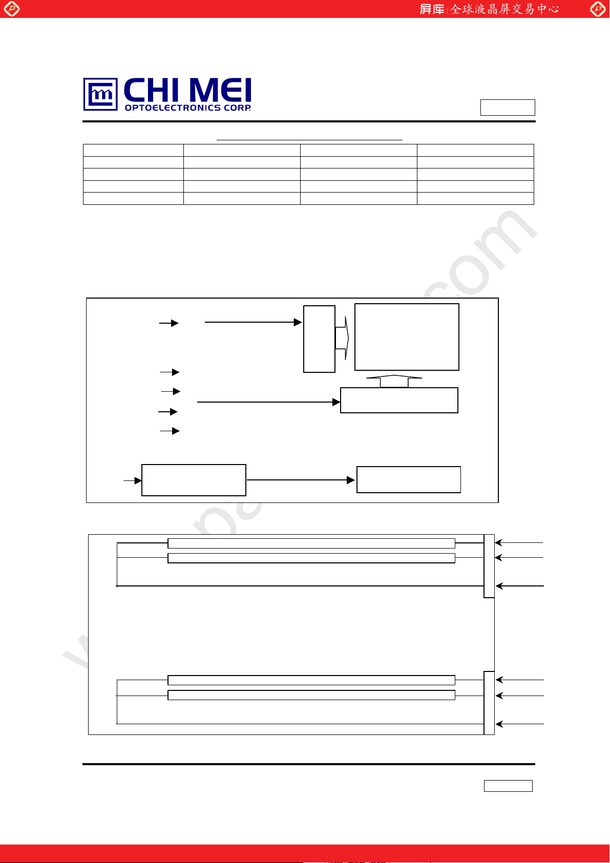
4. INTERFACE SPECIFICATIONS
4.1 Signal Descriptions
Interface Signal CXA1 Interface Signal CXA2
Pin Symbol I/O Function Pin Symbol I/O Function
1 VSA I 1 RPS2 TFT test pin
VSA
2
VSA
3
VSA
4
VSA
5
6 GND - Ground 6 D01 I
7 GND 8 GND -
9 GND 10 - - NC 10 D05 I
11 - - NC 11 D06 I
12 - - NC 12 D07 I
13 LR I
14 VSD
15 LP I
16 RS I
17 SHC I
18 D30 I 18 D15 I
19 D31 I 19 D16 I
20 D32 I 20 D17 I
21 D33 I 21 D20 I
22 D34 I 22 D21 I
23 D35 I 23 D22 I
24 D36 I 24 D23 I
25 D37 I 25 D24 I
26 D40 I 26 D25 I
27 D41 I 27 D26 I
28 D42 I 28 D27 I
29 D43 I 29 RV1 I
30 D44 I
I 2 VCM I
For supply analog power to the
I 3 VCM I
Device.
I 4 GND - Ground
I
Ground
Ground
Ground
For Shift Direction Select
Right shift (Out1-Out384): H
Left shift (Out384-Out1): L
For supply digital power the
Device.
Select the charge /discharge
current level
LP=”H” : Low current level
LP=”L” : Normal current level
Switch LCD drive capability
RS=”H” : For the heavy load
RS=”L” : For the specification load
Control the output circuit
For Data input
Input gray scale data (8 bit)
multiple 2 pixels (6 dot) 48 bit
length image data
Dn0: LSB, Dn7: MSB
www.panelook.com
5 D00 I
7 D02 I
8 D03 I
9 D04 I
13 D10 I
14 D11 I
15 D12 I
16 D13 I
17 D14 I
30 RV2 I
Issue Date: July.02’2001
Model: M170E1 -02
Approval
Panel common voltage
For Data input
Input gray scale data (8 bit)
multiple 2 pixels (6 dot) 48 bit
length image data
Dn0: LSB, Dn7: MSB
Select the input data invert or not
RV1: For port 1 inverting control
RV2: For port 2 inverting control
RV1,2=”H”: Data are inverted
RV1,2=”L”: Data are not inverted
10/30
Version 3.3
One step solution for LCD / PDP / OLED panel application: Datasheet, inventory and accessory!
www.panelook.com
Page 11

Global LCD Panel Exchange Center
www.panelook.com
Issue Date: July.02’2001
Model: M170E1 -02
Approval
31 D45 I 31 POL I
32 D46 I 32 - - NC
33 D47 I 33 TP1 I
34 D50 I 34 CKH I
35 D51 I 35 MODE - NC
36 D52 I 36 GND - Ground
37 D53 I 37 GM1 I
38 D54 I 38 GM2 I
39 D55 I 39 GM3 I
40 D56 I 40 GM4 I
41 D57 I
42 VCM I 42 GM6 I
43 VCM I
44 STH I
45 RPS1 TFT test pin 45 GND - Ground
Pin Symbol I/O Function Pin Symbol I/O Function
1 VSA I
2 GM9 I 2 VCM I
3 GM10 I 3 VCM I
4 GM11 I 4 - - NC
5 GM12 I 5 D00 I
6 GM13 I 6 D01
7 GM14 I 7 D02
8 GM15 I 8 D03
9 GM16 I
10 - - NC 10 D05
11 - - NC 11 D06
12 - - NC 12 D07
Panel common voltage
For Start Pulse I/O of internal Shift
Register
Interface Signal CXB1 Interface Signal CXB2
For supply analog power to the
Device.
For supply ӫCorrection Power
to the Device. Keep the reference
voltage during output gray scale
voltage.
41 GM5 I
43 GM7 I
44 GM8 I
1 RPS4 TFT test pin
9 D04
POL=”L” : The reference voltages
for Odd number outputs are
GMA1~GMA8 Even number
outputs are GMA9~GMA16
POL=”H” : The reference voltages
for Odd number outputs are
GMA9~GMA16 Even number
outputs are GMA1~GMA8
Latch the contents of the data
register and transfer to D/A
converter at the rising edge and
output gray scale voltage at falling
edge.
For transfer the Shift Register
Data Clock input. Write the data
register at the rising edge. CKH
should be input continuously.
For supply ӫCorrection Power to
the Device. Keep the reference
voltage during output gray scale
voltage.
Panel common voltage
For Data input
Input gray scale data (8 bit)
I
multiple 2 pixels (6 dot) 48 bit
I
length image data
I
Dn0: LSB, Dn7: MSB
I
I
I
I
11/30
Version 3.3
One step solution for LCD / PDP / OLED panel application: Datasheet, inventory and accessory!
www.panelook.com
Page 12

Global LCD Panel Exchange Center
www.panelook.com
Issue Date: July.02’2001
Model: M170E1 -02
Approval
For Shift Direction Select
13 L/R I
14 VSD I
15 LP I
16 RS I
17 SHC I
18 D30 I 18 D15
19 D31 I 19 D16
20 D32 I 20 D17
21 D33 I 21 D20
22 D34 I 22 D21
23 D35 I 23 D22
24 D36 I 24 D23
25 D37 I 25 D24
26 D40 I 26 D25
27 D41 I 27 D26
28 D42 I 28 D27
29 D43 I 29 RV1 I
30 D44 I 30 RV2 I
31 D45 I 31 POL
32 D46 I 32 - - NC
33 D47 I 33 TP1
34 D50 I 34 CKH I
35 D51 I 35 MODE - NC
36 D52 I
Right shift (Out1-Out384): H
Left shift (Out384-Out1): L
For supply digital power the
Device.
Select the charge /discharge
current level
LP=”H” : Low current level
LP=”L” : Normal current level
Switch LCD drive capability
RS=”H” : For the heavy load
RS=”L” : For the specification
load
Control the output circuit
For Data input
Input gray scale data (8 bit)
multiple 2 pixels (6 dot) 48 bit
length image data
Dn0: LSB, Dn7: MSB
13 D10
14 D11
15 D12
16 D13
17 D14
36 GND - Ground
12/30
I
I
I
I
I
I
I
I
I
I
I
I
I
I
I
I
Select the input data invert or not
RV1: For port 1 inverting control
RV2: For port 2 inverting control
RV1,2=”H”: Data are inverted
RV1,2=”L”: Data are not inverted
POL=”L” : The reference
voltages for Odd number outputs
are GMA1~GMA8 Even number
outputs are GMA9~GMA16
POL=”H” : The reference
I
voltages for Odd number outputs
are GMA9~GMA16 Even
number outputs are
GMA1~GMA8
Latch the contents of the data
register and transfer to D/A
converter at the rising edge and
I
output gray scale voltage at
falling edge.
For transfer the Shift Register
Data Clock input. Write the data
register at the rising edge. CKH
should be input continuously.
Version 3.3
One step solution for LCD / PDP / OLED panel application: Datasheet, inventory and accessory!
www.panelook.com
Page 13

Global LCD Panel Exchange Center
www.panelook.com
Issue Date: July.02’2001
Model: M170E1 -02
Approval
37 D53 I 37 VSD I
38 D54 I 38 VSD I
39 D55 I 39 VSD I
40 D56 I 40 GND - Ground
41 D57 I
42 STH I
43 RPS3 TFT test pin 43 GND - Ground
44 VCM I 44 GND - Ground
45 VCM I
For Start Pulse I/O of internal
Shift Register
Panel common voltage
For supply digital power the
Device.
41 GND - Ground
42 GND - Ground
45 GND - Ground
13/30
Version 3.3
One step solution for LCD / PDP / OLED panel application: Datasheet, inventory and accessory!
www.panelook.com
Page 14

Global LCD Panel Exchange Center
Interface Signal CNY1 Interface Signal CNY1
Pin Symbol I/O Function Pin Symbol I/O Function
1 VGH I- 11 CKV I
2 VGH I
3 GND - Ground 13 VAA I VSA
4 GND - Ground 14 RPG4 TFT test pin
5 VGL I 15 RPG3
6 VGL I
7 VGD - 17 RPG1
8 VGD -
9 STV I Vertical shift data control signal 19 VCM O Panel common voltage
10 OE I
Power supply for LCD drive
Analog input pins. These pins
accept as their input the OFF
level at the LCD panel drive pins.
Power supply for the internal logic
Output enable pins. This signals
control the data appearing at the
LCD panel drive pins. The VGH/L
voltage is output when OE are
high; normal shift data is output
when OE are low.
www.panelook.com
12 GND - Ground
16 RPG2
18 VREF I Reference voltage
20 VCM O Panel common voltage
Upper Side
CXB2 CXB1 CXA2 CXA1
LCD Module
Rear Side
Lower Side
Issue Date: July.02’2001
Model: M170E1 -02
Approval
Vertical shift clock. This is the
shift clock for the shift registers.
Data is shifted though the shift
registers synchronously with the
rising edge of CKV
TFT test pin
TFT test pin
TFT test pin
CNY1
14/30
Version 3.3
One step solution for LCD / PDP / OLED panel application: Datasheet, inventory and accessory!
www.panelook.com
Page 15

Global LCD Panel Exchange Center
4.2 Input Signal Timing
AC(In case of 3.0VЉЉЉЉVSDІІІІ3.6)
Parameter Symbol Condition Min Typ Max Unit
CKH Pulse Width t1 14 ns
CKH High Level Width t2 2 ns
CKH Low Level Width t3 2 ns
Data/REV Setup Time t4 2 ns
Data/REV Hold Time t5 0 ns
Start Pulse Setup Time t6 2 ns
Start Pulse Hold Time t7 0 ns
TP1 signal to EI0(input) signal Setup
Time
CKH of Tail Data to TP1(L) Hold Time t18 1 CKH count
TP1 signal High Level Width t20 1.5
POL signal to TPI signal Setup Time t21 -5
TP1 signal to POL signal Hold Time t22 6.0 ns
TP1 signal to SHC signal Hold Time t25 4.5
SHC signal to TP1 signal Setup Time t26 4.5
www.panelook.com
Issue Date: July.02’2001
Model: M170E1 -02
Approval
t17 70 ns
Ӵ
s
Ӵs
Ӵs
15/30
Version 3.3
One step solution for LCD / PDP / OLED panel application: Datasheet, inventory and accessory!
www.panelook.com
Page 16

Global LCD Panel Exchange Center
Timing Chart
www.panelook.com
Issue Date: July.02’2001
Model: M170E1 -02
Approval
CKH
Dxx
REV1
RV2
TP1(L/R=H)or
STH(L/R=L)
Input Signal
CKH
TP1(L/R=H)or
STH(L/R=L)
Input Signal
TP1
t1
64
t18
t2 t3
t4 t5
t6 t6 t7 t7
t17
1 63 64
~
~
~
~ ~
~
~
~
t20
64631 2
POL
TP1
SHC
t21 t22
t25 t25 t26
16/30
Version 3.3
One step solution for LCD / PDP / OLED panel application: Datasheet, inventory and accessory!
www.panelook.com
Page 17

Global LCD Panel Exchange Center
The Relationship between Input Data and Output
www.panelook.com
Issue Date: July.02’2001
Model: M170E1 -02
Approval
Dnn
TP1
SHC
Output
Line n Line n+1 Line n+2 Line n+3 Line n+4
Line n+1 Line n+2 Line n Line n-1 Line n-2
17/30
Version 3.3
One step solution for LCD / PDP / OLED panel application: Datasheet, inventory and accessory!
www.panelook.com
Page 18

Global LCD Panel Exchange Center
AC Characteristic(Reference to VGH= 25 to 42V, VDD= 3.0 to 16V, Ta= -20 to 75кккк
unless otherwise noted)
Parameter Symbol Test Circuit Test Condition Min. Typ. Max. Unit
Clock Period tCPV - - 10 - -
CKV Pulse Width (H) tCPVH - - 4 - CKV Pulse Width (L) tCPVL - - 4 - Data Set-up Time tsDI - - 1 - Data Hold Time thDI - - 1 - OE Enable Time tWOE - - 1 - Output Delay Time (2) tpdG - CL=300pF - - 1
Output Delay Time (3) tpdOE - CL=300pF - - 1
www.panelook.com
Issue Date: July.02’2001
Model: M170E1 -02
Approval
Ӵs
Ӵs
Ӵs
Ӵ
s
Ӵs
Ӵs
Ӵs
Ӵ
s
18/30
Version 3.3
One step solution for LCD / PDP / OLED panel application: Datasheet, inventory and accessory!
www.panelook.com
Page 19

Global LCD Panel Exchange Center
50%
50%
50%
50%
Timing Chart
www.panelook.com
Issue Date: July.02’2001
Model: M170E1 -02
Approval
CKV
STV
CKV
tCPVH
tCPVL
tsDI
tpdG
tCPV
thDI
tpdG
VGH
VGL
tpdGtpdG
VGH
VGL
VGH
VGL
tWOE
OE
tpdOE
tpdOE
19/30
Version 3.3
One step solution for LCD / PDP / OLED panel application: Datasheet, inventory and accessory!
VGH
VGL
www.panelook.com
Page 20

Global LCD Panel Exchange Center
Power Sequence Spec.
Voltage should be met the following
www.panelook.com
Issue Date: July.02’2001
Model: M170E1 -02
Approval
t2
VGH
GND
VSD/VGD
10msЉt2Љ250ms
t1, t3Њ1.5ms
90%
t1
10%
VSA
VREF
Signal
VGL
t3
10%
10%
20/30
Version 3.3
One step solution for LCD / PDP / OLED panel application: Datasheet, inventory and accessory!
www.panelook.com
Page 21

Global LCD Panel Exchange Center
4.3 COLOR DATA INPUT ASSIGNMENT
Color
R7 R6 R5 R4 R3 R2 R1 R0 R7 R6 G5 G4 G3 G2 G1 G0 R7 R6 B5 B4 B3 B2 B1 B0
0
1
0
0
0
1
1
1
0
0
0
:
:
1
1
1
Basic
Colors
Gray
Scale
Of
Red
Black
Red
Green
Blue
Cyan
Magenta
Yellow
White
Red(0) / Dark
Red(1)
Red(2)
:
:
Red(253)
Red(254)
Red(255)
www.panelook.com
Issue Date: July.02’2001
Model: M170E1 -02
Approval
Data Signal
Red Green Blue
0
0
0
0
0
0
0
0
1
1
0
0
0
0
0
0
1
1
1
1
1
1
0
0
0
0
0
0
:
:
:
:
1
1
1
1
1
1
0
0
1
1
0
0
0
0
0
0
1
1
1
1
1
1
0
0
0
0
0
0
:
:
1
1
1
1
1
1
0
0
0
1
1
1
1
0
0
0
0
0
0
0
1
1
1
1
1
1
0
0
0
0
0
1
:
:
:
:
1
0
1
1
1
1
0
0
1
0
0
1
1
1
1
1
0
0
0
1
0
0
:
:
:
:
:
:
0
1
0
0
0
1
0
0
0
0
0
0
0
0
1
1
1
1
0
0
0
0
1
1
1
1
0
0
0
0
1
1
1
1
1
1
1
1
0
0
0
0
0
0
0
0
0
0
0
0
:
:
:
:
:
:
:
:
0
0
0
0
0
0
0
0
0
0
0
0
0
0
0
0
1
1
0
0
1
1
0
0
1
1
1
1
0
0
0
0
0
0
:
:
:
:
0
0
0
0
0
0
0
0
0
0
0
0
0
0
1
1
1
0
1
1
1
1
1
0
0
0
1
1
1
1
0
0
0
0
0
0
0
0
0
:
:
:
:
0
0
0
0
0
0
0
0
0
0
0
0
0
0
0
0
0
0
0
0
0
0
0
1
1
1
1
1
1
1
1
1
1
1
1
1
1
1
1
1
1
0
0
0
0
0
0
1
1
1
1
1
1
0
0
0
0
0
0
0
0
0
0
0
0
0
0
0
0
0
0
:
:
:
:
:
:
:
:
:
:
:
:
:
:
0
0
0
0
0
0
0
0
0
0
0
0
0
0
0
0
0
0
Gray
Scale
Of
Green
Gray
Scale
Of
Blue
Green(0) / Dark
Green(1)
Green(2)
:
:
Green(253)
Green(254)
Green(255)
Blue(0) / Dark
Blue(1)
Blue(2)
:
:
Blue(253)
Blue(254)
Blue(255)
0
0
0
0
0
0
0
0
0
0
0
0
0
0
0
0
0
0
0
0
0
0
0
0
0
0
0
0
0
0
0
0
1
0
0
0
0
0
0
0
0
0
0
0
0
0
0
0
0
0
0
0
0
0
0
0
0
1
0
0
0
0
0
0
0
0
0
0
0
0
0
0
:
:
:
:
:
:
:
:
:
:
:
:
:
:
:
:
:
:
:
:
:
:
:
:
:
:
:
:
:
:
:
:
:
:
:
:
:
:
:
:
:
:
:
:
:
:
:
:
0
0
0
0
0
0
0
0
1
0
1
1
1
1
1
1
0
0
0
0
0
0
0
0
0
0
0
0
0
0
0
0
0
1
1
1
1
1
1
1
0
0
0
0
0
0
0
0
0
0
0
0
0
0
0
0
1
1
1
1
1
1
1
1
0
0
0
0
0
0
0
0
0
0
0
0
0
0
0
0
0
0
0
0
0
0
0
0
0
0
0
0
0
0
0
0
1
0
0
0
0
0
0
0
0
0
0
0
0
0
0
0
0
0
0
0
0
0
0
0
0
1
0
0
0
0
0
0
0
0
0
0
0
0
0
0
0
0
0
0
0
0
0
0
:
:
:
:
:
:
:
:
:
:
:
:
:
:
:
:
:
:
:
:
:
:
:
:
:
:
:
:
:
:
:
:
:
:
:
:
:
:
:
:
:
:
:
:
:
:
:
:
0
1
1
1
1
1
1
1
0
0
0
0
0
0
0
0
0
0
0
0
0
0
0
0
1
0
1
1
1
1
1
1
0
0
0
0
0
0
0
0
0
0
0
0
0
0
0
0
1
1
1
1
1
1
1
1
0
0
0
0
0
0
0
0
0
0
0
0
0
0
0
0
21/30
Version 3.3
One step solution for LCD / PDP / OLED panel application: Datasheet, inventory and accessory!
www.panelook.com
Page 22

Global LCD Panel Exchange Center
5. OPTICAL CHARACTERISTICS
5.1 TEST CONDITIONS
Item Symbol Value Unit
Ambient Temperature Ta 25±2
Ambient Humidity Ha 50±10 %RH
Supply Voltage Vcc 5.0 V
Input Signal According to typical value in "Electrical Characteristics"
Inverter Current IL 13.0 mA
Inverter Driving Frequency FL 40 K Hz
Inverter Sumida H05-4785
The measuring method is shown in 5.2 OPTICAL SPECIFICATIONS. The following items are
measured under stable conditions about 20 minutes after the module works. The optical characteristics
should be measured under lamp current I
equivalent state with the methods shown in Note (6).
www.panelook.com
Issue Date: July.02’2001
Model: M170E1 -02
Approval
o
C
= 13.0 m Arms and in a dark environment ( 2 lux) or
L
5.2 OPTICAL SPECIFICATIONS
Item
Contrast Ratio CR 250 300 - - (2),(6)
Red
Green
Blue
White
Hor.
Ver.
Response Time
Luminance of white
(Average Luminance)
Cross Talk CT - - 5.0 % (5),(6)
Luminance
Uniformity
Chromaticity
Viewing Angle
White Variation
Symbol
t
ON
t
OFF
L
AVE
Rx 0.61 0.63 0.65
Ry 0.34 0.36 0.38
Gx 0.28 0.30 0.32
Gy 0.57 0.59 0.61
Bx 0.13 0.15 0.17
By 0.07 0.09 0.11
Wx 0.30 0.32 0.34
Wy
θ
+
x
θ
x
θY+
θ
Y
δW
Conditions
=0°, θY =0°
θ
x
Viewing normal angle
-
-
Viewing normal angle
CR=5
θ
=0°, θY =0°
x
Specifications
Min. Typ. Max.
- 15 30 ms
- 35 50 ms
200 230 - cd/m2 (4),(6)
0.31 0.33 0.35
70 80 -
70 80 -
50 60 -
70 80 -
- 20 30 % (6),(8)
Deg.
Unit
Note
(3)
(1), (6)
22/30
Version 3.3
One step solution for LCD / PDP / OLED panel application: Datasheet, inventory and accessory!
www.panelook.com
Page 23

Global LCD Panel Exchange Center
Note (1) Definition of Viewing Angle θx, θy:
www.panelook.com
Issue Date: July.02’2001
Model: M170E1 -02
Approval
θX- = 90º
6 o’clock
y- = 90º
θ
x-
y-
Normal
θx = θy = 0º
θy- θy+
θx−
y+
θx+
Note (2) Definition of Contrast Ratio:
The contrast ratio can be calculated by the following expression.
Contrast Ratio (CR) = L255 / L0
L255: Luminance on the white raster (gray level 255)
L 0: Luminance on the black raster (gray level 0)
12 o’clock direction
y+
= 90º
θ
x+
θX+ = 90º
CR
= CR (5)
CR (X) is corresponding to the Contrast Ratio of the point X at Figure in Note (7).
Note (3) Definition of Response time:
100%
90%
Optical
Response
10%
0%
Gray level 255
Tr
Gray level 0
Tf
Gray level 255
time
23/30
Version 3.3
One step solution for LCD / PDP / OLED panel application: Datasheet, inventory and accessory!
www.panelook.com
Page 24

Global LCD Panel Exchange Center
A
A
(0, 0)
(
)
Note (4) Definition of Average Luminance of White:
Measure the luminance of gray level 255 at 5 points
L
= [L (1)+ L (2)+ L (3)+ L (4)+ L (5)] / 5
AVE
Note (5) Definition of Cross Talk (CT):
L (x) is corresponding to the luminance of the point X at Figure in Note (7).
www.panelook.com
Issue Date: July.02’2001
Model: M170E1 -02
Approval
CT = | Y
– YA | / YA ×100 (%)
B
Where:
Y
= Luminance of measured location without gray level 0 pattern (cd/m2)
A
Y
= Luminance of measured location with gray level 0 pattern (cd/m2)
B
Y
A,L
Y
(640, 896)
A, D
(0, 0)
(160, 512)
ctive
Gray level 128
Y
(640, 128)
A, U
Y
(1120, 512)
A, R
(1279, 1023)
(320, 256)
Y
(160, 512)
B, L
Y
(640, 896)
B, D
ctive
Gray 0
Gray level 128
Y
(640, 128)
B,U
Y
(1120, 512)
B,R
(960, 768)
1279, 1023
Note (6) Measuring setup:
The measurement supposes to be executed after stabilizing the panel at given temperature during 20
minutes in the case of abrupt temperature change. The measurement shall be executed after lighting at
rating 20 minutes. In order to stabilize the luminance, LCD shall not be gotten winds.
LCD module
LCD panel
Center of the screen
Photometer
(TOPCON BM-5A)
Field of view = 2º
500 mm
24/30
Version 3.3
One step solution for LCD / PDP / OLED panel application: Datasheet, inventory and accessory!
www.panelook.com
Page 25

Global LCD Panel Exchange Center
Note (7) Definition of luminance
www.panelook.com
Issue Date: July.02’2001
Model: M170E1 -02
Approval
Horizontal Line Number
0
0
320 640 960 1279
256
1
2
Vertical Line Number
512
768
1023
3
5
4
Active area
Horizontal Line Number [pixel]
Note (8) Definition of luminance uniformity δW (9 points, gray level 255):
δW = 100%[ Lmax – Lmin ] / Lmax = 100% [1 – Lmin / Lmax]
H/10
H/2 H/2
H/10
1 3
2
V
4
5
6
7
98
H
Active area
V/10
V/10
V/2
V/2
X
X
: test point
X=1 to 5
: test point
X
X=1 to 9
6. MECHNICAL DRAWING
Please refer to the attached drawings.
25/30
Version 3.3
One step solution for LCD / PDP / OLED panel application: Datasheet, inventory and accessory!
www.panelook.com
Page 26

Global LCD Panel Exchange Center
7. PRECAUTION
7. 1 ASSEMBLY AND HANDLING PRECAUTION
(1) Do not apply rough force such as bending or twisting to the module during assembly.
(2) To assembly and install module into user’s system are only in clean working areas. The dust and oil
may cause an electrical short or worsen the polarizer.
(3) It’s not permitted to pressure or impulse the module because the LCD panel and backlight,
(4) Always follow the correct power sequence when user connects and operates the LCD module to
prevent damage to the CMOS LSI chips during latchup.
(5) Do not pull the I/F connectors in or out while the module is operation.
(6) Do not disassembly the module.
(7) Use a soft dry cloth without chemicals for cleaning, because the surface of polarizer is very soft and
easily scratched.
(8) Any moisture come into contact with the LCD module is dangerous because LCD modules is turned
on with moisture on its surface may cause it damage.
(9) The high temperature or humidity may reduce the performance of module, to store LCD module
within the specified storage condition.
(10) The ambient temperature is lower than 10ºC may reduce the display quality, for example, response
time become slowly, the starting voltage of CCFL is higher than room temperature.
www.panelook.com
Issue Date: July.02’2001
Model: M170E1 -02
Approval
7.2 SAFETY PRECAUTION
(1) The startup voltage of backlight is approximately 1000 Volts. It may cause electrical shock during
assembly with inverter. Do not disassemble the module or insert anything into the backlight unit.
(2) If the liquid crystal material leaks from the panel, it should be kept away from the eyes or mouth. In
case of contact with hands, skin or clothes, it has to be washed away thoroughly with soap.
(3) After the module’s end of life, it is not harmful in case of normal operation and storage.
26/30
Version 3.3
One step solution for LCD / PDP / OLED panel application: Datasheet, inventory and accessory!
www.panelook.com
Page 27

Global LCD Panel Exchange Center
8. PACKAGING
8.1 PACKING SPECIFICATIONS
(1) 5 LCD modules / 1 Box
(2) Box dimensions : 534(L) X 316(W) X 462(H) mm
(3) Weight : approximately 8.0Kg ( 5 modules per box)
8.2 PACKING Method
Figures 8-1and 8-2 are the packing method.
www.panelook.com
Issue Date: July.02’2001
Model: M170E1 -02
Approval
Figure. 8-1 Packing method
27/30
Version 3.3
One step solution for LCD / PDP / OLED panel application: Datasheet, inventory and accessory!
www.panelook.com
Page 28

Global LCD Panel Exchange Center
www.panelook.com
Issue Date: July.02’2001
Model: M170E1 -02
Approval
Figure. 8-2 Packing method
28/30
Version 3.3
One step solution for LCD / PDP / OLED panel application: Datasheet, inventory and accessory!
www.panelook.com
Page 29

Global LCD Panel Exchange Center
9. INCOMING INSPECTION DAY
The Supplier should be acquainted the inspection results (acceptance or rejection) by Customer,
and the results are in accordance with the incoming inspection standard within 30 days after the date
of the bills of lading.
Should Customer fail to so notify the Supplier within the said 30 days period. The Customer’s right to
reject the LCMS shall then lapse, and the said LCMS shall be deemed to have been accepted by the
customer.
www.panelook.com
Issue Date: July.02’2001
Model: M170E1 -02
Approval
29/30
Version 3.3
One step solution for LCD / PDP / OLED panel application: Datasheet, inventory and accessory!
www.panelook.com
Page 30

Global LCD Panel Exchange Center
10. Definition of Shipping Label on Module
The barcode nameplate is pasted on each module as illustration, and its
definition is as following explanation.
www.panelook.com
Issue Date: July.02’2001
Model: M170E1 -02
Approval
M170E1 -02 Rev. XX
(1) Model Name: M170E1 -02
(2) Revision Rev.XX
(3) Serial ID: 0 8
Serial ID include the information as list.
1. Manufactured Date:
2. Revision Code: cover all the change
3. Model code
4. Serial No. : Manufacturing sequence of product
MADE IN TAIWAN
XXXXXXXXXXXXXXX
XX 0 0 2 X X X 1 X X X X
Year: 0~9, for 2000~2009
Month: 0~9, A~C, for Jan. ~ Dec.
Day: 0~9, A~Y, for 1
st
to 31st, exclude I and O
E207943
MADE IN TAIWAN
Serial No.
Product Line
Year, Month, Date
CMO Internal Use
CMO Internal Use
Revision A1
Model Code
4. Product Line : 1 -> Line1, 2 -> Line 2 …,etc.
30/30
Version 3.3
One step solution for LCD / PDP / OLED panel application: Datasheet, inventory and accessory!
www.panelook.com
Page 31

Global LCD Panel Exchange Center
www.panelook.com
One step solution for LCD / PDP / OLED panel application: Datasheet, inventory and accessory!
www.panelook.com
Page 32

Global LCD Panel Exchange Center
www.panelook.com
E207943
One step solution for LCD / PDP / OLED panel application: Datasheet, inventory and accessory!
www.panelook.com
 Loading...