

Page 1
Global LCD Panel Exchange Center
www.panelook.com
One step solution for LCD / PDP / OLED panel application: Datasheet, inventory and accessory!
www.panelook.com
Page 2
Global LCD Panel Exchange Center
www.panelook.com
Issued Date:Jan.15’2003
Model No.: M150X3-T03
Approval
- CONTENTS -
REVISION HISTORY
1. GENERAL DESCRIPTION
1.1 OVERVIEW
1.2 FEATURES
1.3 APPLICATION
1.4 GENERAL SPECIFICATIONS
1.5 MECHANICAL SPECIFICATIONS
2. ABSOLUTE MAXIMUM RATINGS
2.1 ABSOLUTE RATINGS OF ENVIRONMENT
2.2 ELECTRICAL ABSOLUTE RATINGS
2.2.1 TFT LCD MODULE
2.2.2 BACKLIGHT UNIT
3. ELECTRICAL CHARACTERISTICS
3.1 TFT LCD MODULE
3.2 BACKLIGHT UNIT
4. BLOCK DIAGRAM
4.1 TFT LCD MODULE
4.2 BACKLIGHT UNIT
5. INPUT TERMINAL PIN ASSIGNMENT
5.1 TFT LCD MODULE
5.2 BACKLIGHT UNIT
5.3 COLOR DATA INPUT ASSIGNMENT
6. INTERFACE TIMING
6.1 INPUT SIGNAL TIMING SPECIFICATIONS
6.2 POWER ON/OFF SEQUENCE
7. OPTICAL CHARACTERISTICS
7.1 TEST CONDITIONS
7.2 OPTICAL SPECIFICATIONS
8. PRECAUTIONS
8.1 HANDLING PRECAUTIONS
8.2 STORAGE PRECAUTIONS
8.3 OPERATION PRECAUTIONS
9. PACKAGING ------------------------------------------------------- 21
9.1 PACKING SPECIFICATIONS
9.2 PACKING METHOD
10. INCOMING INSPECITION DAY ------------------------------------------------------- 23
11. DEFINITION OF SHIPPING LABEL ON MODULE ------------------------------------------------------- 24
------------------------------------------------------- 3
------------------------------------------------------- 4
------------------------------------------------------- 5
------------------------------------------------------- 7
------------------------------------------------------- 10
------------------------------------------------------- 11
------------------------------------------------------- 13
------------------------------------------------------- 16
------------------------------------------------------- 19
2 / 25
One step solution for LCD / PDP / OLED panel application: Datasheet, inventory and accessory!
Version 3.1
www.panelook.com
Page 3

Global LCD Panel Exchange Center
www.panelook.com
Issued Date:Jan.15’2003
Model No.: M150X3-T03
Approval
Version Date
Ver 0.0
Ver 0.1
Ver 1.0
Ver 2.0
Ver.2.1
Apr.10’2001
Apr.30’2001
May.15’2001
May.15’2001
May.23’2001
Page
(New)
All
10
17
14
17
21~22
23
24
All
17
All
REVISION HISTORY
Section Description
Tentative Specification was first issued.
All
Update LVDS input to TTL input.
4.1
Update inverter current: 6.0mA Æ 5.5mA
7.1
Update Color Chromaticity: Rx: TBD(Typ.)Æ(0.629)(Typ.)
4
7
7
9
7.2
1.2
3.1
6.1
7.2
9
10
11
All
7.2
All
2.2.1
2.2.2
3.2
Ry: TBD(Typ.)Æ(0.355)(Typ.)
Gx: TBD(Typ.)Æ(0.290)(Typ.)
Gy: TBD(Typ.)Æ(0.593)(Typ.)
Bx: TBD(Typ.)Æ(0.142)(Typ.)
By: TBD(Typ.)Æ(0.094)(Typ.)
Update TTL Interface with 1pixels/clock to 2 pixels/clock
Update Ripple Voltage: TBD(Typ.) Æ -(Typ.)
Rush Current: -(Typ.)/TBD(Max.)Æ480(Typ.)/525(Max.)
Power Supply Currrent:
White: TBD(Typ.)/-(Max.)Æ350(Typ.)/380(Max.)
Black: TBD(Typ.)/-(Max.)Æ530(Typ.)/570(Max.)
Vertical Stripe: TBD(Typ.)/-(Max.)Æ450(Typ.)/480(Max.)
Differential Input Voltage for LVDS Receiver Threshold:
“H” Level: 2.64(Min.)/Vcc(Max.)Æ2.4(Min.)/3.6(Max.)
“L” Level: GND(Min.)/0.6(Max.)Æ0(Min.)/0.6(Max.)
Delete Terminating Resistor.
Update Pixel clock period:
20(Min.)/15(Typ.)/12.5(Max.)Æ12.5(Min.)/15(Typ.)/20(Max.)
Update Response Time: T
T
: 15(Typ.)/30(Max.)Æ7(Typ.)/22(Max.)
R
: 35(Typ.)/50(Max.)Æ23(Typ.)/38(Max.)
F
Update Color Chromaticity:
Rx:-(Min.)/(0.629)(Typ.)/-(Max.) Æ(0.607)(Min.)/(0.637)(Typ.)/(0.667)(Max.)
Ry: -(Min.)/(0.355)(Typ.)/-(Max.) Æ(0.323)(Min.)/(0.353)(Typ.)/(0.383)(Max.)
Gx:-(Min.)/(0.290)(Typ.)/-(Max.) Æ(0.272)(Min.)/(0.302)(Typ.)/(0.332)(Max.)
Gy: -(Min.)/(0.593)(Typ.)/-(Max.) Æ(0.558)(Min.)/(0.588)(Typ.)/(0.618)(Max.)
Bx: -(Min.)/(0.142)(Typ.)/-(Max.) Æ(0.111)(Min.)/(0.141)(Typ.)/(0.171)(Max.)
By: -(Min.)/(0.094)(Typ.)/-(Max.) Æ(0.064)(Min.)/(0.094)(Typ.)/(0.124)(Max.)
Add 9. PACKAGING
Add 10. INCOMING INSPECTION DAY
Add 11. DEFINITION OF SHIPPING LABEL ON MODULE.
Approval Specification was issued.
Update Color Chromaticity (take away parentheses).
Change Vcc to V
DD.
Update Power Supply Voltage: Vss-0.3(Min.) Æ -0.3(Min.)
Update Lamp Voltage:(640)(Min)/(800)(Max) Æ603(Min)/737(Max)
Update Lamp Input Voltage:
(640)(Min.)/(720)(Typ.)/(800)(Max.)Æ603(Min.)/670(Typ.)/737(Max.)
Update Lamp Turn On Voltage:25
o
C:(1150)Æ870/ 0oC:(1500)Æ1090
3 / 25
One step solution for LCD / PDP / OLED panel application: Datasheet, inventory and accessory!
Version 3.1
www.panelook.com
Page 4
Global LCD Panel Exchange Center
www.panelook.com
Issued Date:Jan.15’2003
Model No.: M150X3-T03
Approval
Version Date
Ver 2.1
Ver 3.0
Ver 3.1
May.23’2001
Jun.06’2001
Jan.15’2003
Page
(New)
9
10
11
15
18
25
All
8
18
REVISION HISTORY
Section Description
Update Lamp Life Time: 50000(Min.)Æ40000(Min.)/50000(Typ.)
3.2
Update Power Consumption: (9360)(Typ.)Æ14740(Typ.)
Update Note (5): I
-
4.1
Update Input Signal.
6.1
Update Pixel clock frequency: 65(Typ.)/80(Max.)Æ32.5(Typ.)/40(Max.)
7.1
7.2
11
All
3.1
7.2
clock period:12.5(Min.)/15(Typ.)/20(Max.)Æ25(Min.)/30(Typ.)/40(Max.)
Update Horizontal display active period:
1024(Min.)/1024(Typ.)/1024(Typ.)Æ512(Min.)/512(Typ.)/512(Max.)
Update Horizontal display blank period:
76(Min.)/320(Typ.)/776(Max.)Æ38(Min.)/160(Typ.)/388(Max.)
Update Horizontal period:
1100(Min.)/1344(Typ.)/1800(Typ.)Æ550(Min.)/672(Typ.)/900(Max.)
Update Supply Voltage: 5.0VÆ3.3V
Update Color Chromaticity:
Wx: -(Min.)/0.310(Typ.)/-(Max.)Æ0.280(Min.)/0.310(Typ.)/0.340(Max.)
Wy: -(Min.)/0.330(Typ.)/-(Max.)Æ0.300(Min.)/0.330(Typ.)/0.360(Max.)
Update shipping label.
Issue approval spec. for PRO ARCH TECHNOLOGY INC.
Delete Ripple Voltage.
Update Rush Current: 480mA(Typ.)/525mA(Max.)Æ -(Typ.)/1.5A(Max.)
Update Note(2) V
Center Luminance of WhiteΚ250(Typ.)Æ300(Typ.)
= 7.0mA Æ IL = 6.5mA
L
rising time to 470Ӵs.
DD
4 / 25
One step solution for LCD / PDP / OLED panel application: Datasheet, inventory and accessory!
Version 3.1
www.panelook.com
Page 5
Global LCD Panel Exchange Center
1. GENERAL DESCRIPTION
1.1 OVERVIEW
M150X3-T03 is a 15.0” TFT Liquid Crystal Display module with 4 CCFL Backlight units and 60 pins TTL
interface. This module supports 1024 x 768 XGA mode and can display 262,144. The optimum viewing
angle is at 6 o’clock direction. The inverter module for Backlight is not built in.
1.2 FEATURES
- XGA (1024 x 768 pixels) resolution
- DE (Data Enable) only mode
-TTL Interface with 2pixels/clock
1.3 APPLICATION
www.panelook.com
Issued Date:Jan.15’2003
Model No.: M150X3-T03
Approval
- Desktop monitors
1.4 GENERAL SPECIFICATI0NS
Item Specification Unit Note
Active Area 304.1(H) x 228.1(V) (15.0” diagonal) mm
Bezel Opening Area 308.2(H) x 232.1(V) mm
Driver Element a-Si TFT active matrix - Pixel Number 1024 x R.G.B. x 768 pixel Pixel Pitch 0.297(H) x 0.297(W) mm Pixel Arrangement RGB vertical stripe - Display Colors 262,144 color Transmissive Mode Normally white - -
1.5 MECHANICAL SPECIFICATIONS
Item Min. Typ. Max. Unit Note
Horizontal(H) - 331.6 - mm
Module Size
Note (1) Please refer to the attached drawings for more information of front and back outline dimensions.
Note (2) The depth is without connector.
Vertical(V) - 254.76 - mm
Depth(D) - 13.0 - mm (1)(2)
Weight - - 1,350 g -
(1)
(1)
5 / 25
One step solution for LCD / PDP / OLED panel application: Datasheet, inventory and accessory!
Version 3.1
www.panelook.com
Page 6
Global LCD Panel Exchange Center
2. ABSOLUTE MAXIMUM RATINGS
2.1 ABSOLUTE RATINGS OF ENVIRONMENT
Item Symbol
Storage Temperature TST -20 +60 ºC (1)
Operating Ambient Temperature TOP 0 +50 ºC (1), (2)
Storage Humidity HST 5 85 % Operation Humidity HOP 20 85 % Shock (Non-Operating) S
Vibration (Non-Operating) V
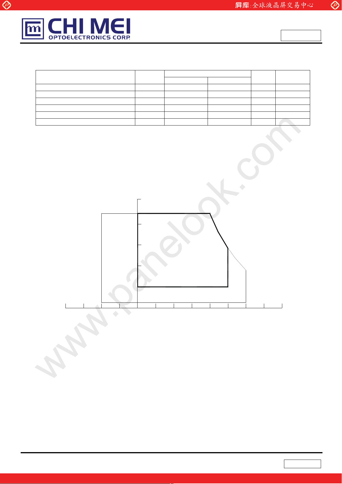
Note (1) Temperature and relative humidity range is shown in the figure below.
(a) 85 %RH Max. (Ta d 40 ºC).
(b) Wet-bulb temperature should be 39 ºC Max. (Ta > 40 ºC).
(c) No condensation of water.
www.panelook.com
Issued Date:Jan.15’2003
Model No.: M150X3-T03
Approval
Value
Min. Max.
- 50 G (3), (5)
NOP
- 2 G (4), (5)
NOP
Unit Note
Relative Humidity (%RH)
100
85
80
60
Operating Range
40
20
Storage Range
5
Temperature (ºC)
8060 -20 400 20-40
Note (2) The temperature of panel surface should be 0 ºC Min. and 60 ºC Max.
Note (3) 6ms, 1 time each rX,rY and rZ directions
Note (4) 10 ~ 500 Hz, 1 cycle/20min. 1.5mm max, 1 hour each X, Y and Z directions
Note (5) At testing Vibration and Shock, the fixture in holding the module has to be hard and rigid enough
so that the module would not be twisted or bent by the fixture.
6 / 25
One step solution for LCD / PDP / OLED panel application: Datasheet, inventory and accessory!
Version 3.1
www.panelook.com
Page 7
Global LCD Panel Exchange Center
2.2 ELECTRICAL ABSOLUTE RATINGS
2.2.1 TFT LCD MODULE
Item Symbol
Power Supply Voltage VDD -0.3 4.0 V
2.2.2 BACKLIGHT UNIT
Item Symbol
Lamp Voltage VL 603 737 V
Lamp Current IL 2.0 6.5 mA
Lamp Frequency FL 30 80 KHz
Note (1) Permanent damage to the device may occur if maximum values are exceeded. Function operation
should be restricted to the conditions described under Normal Operating Conditions.
www.panelook.com
Value
Min. Max.
Value
Min. Max.
Unit Note
Unit Note
Issued Date:Jan.15’2003
Model No.: M150X3-T03
Approval
(1), (2), IL = 5.5 mA
RMS
RMS
(1), (2)
Note (2) Specified values are for lamp (Refer to Section 3.2 for further information).
7 / 25
One step solution for LCD / PDP / OLED panel application: Datasheet, inventory and accessory!
Version 3.1
www.panelook.com
Page 8
Global LCD Panel Exchange Center
3. ELECTRICAL CHARACTERISTICS
3.1 TFT LCD MODULE
Parameter Symbol
Power Supply Voltage VDD 3.0 3.3 3.6 V Rush Current I
White - 350 380 mA (3)a
Power Supply Current
Input voltage
Note (1) The module should be always operated within above ranges.
Note (2) Measurement Conditions:
Black - 530 570 mA (3)b
Vertical Stripe
“H” Level VIH 2.4 - 3.6 V “L” Level V
www.panelook.com
Min. Typ. Max.
- - 1.5 A (2)
RUSH
lcc
- 450 480 mA (3)c
0 - 0.9 V -
IL
Value
Issued Date:Jan.15’2003
Model No.: M150X3-T03
Approval
Unit Note
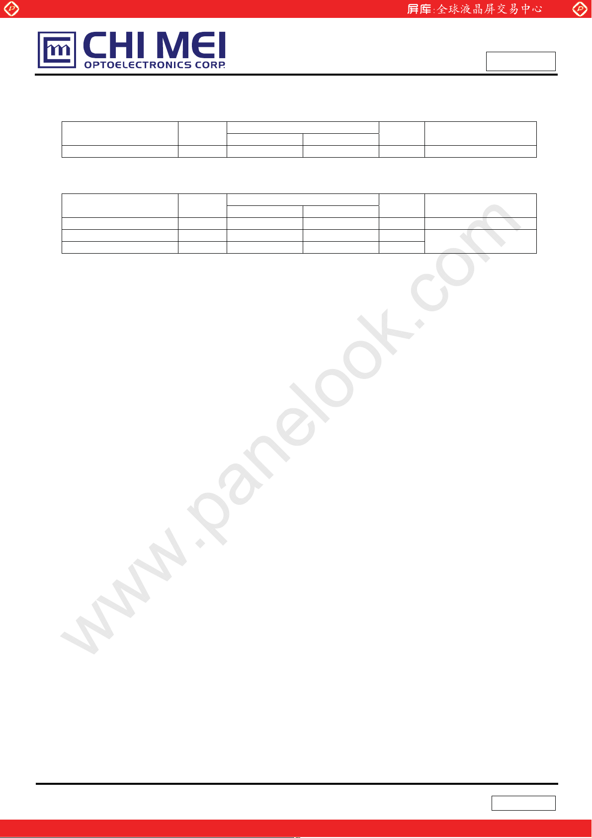
+3.3V
R1
47K
Q1 2SK1475
FUSE
C3
1uF
VDD
(LCD Module Input)
(High to Low)
(Control Signal)
SW
+12V
C1
1uF
VR1
R2
1K
47K
0.01uF
Q2
2SK1470
C2
+3.3V
0.9 V
DD
0.1 VDD
GND
470Ӵs
8 / 25
One step solution for LCD / PDP / OLED panel application: Datasheet, inventory and accessory!
Version 3.1
www.panelook.com
Page 9
Global LCD Panel Exchange Center
Note (3) The specified power supply current is under the conditions at VDD =3.3V, Ta = 25 r 2 ºC, DC
www.panelook.com
Issued Date:Jan.15’2003
Model No.: M150X3-T03
Approval
Current and f
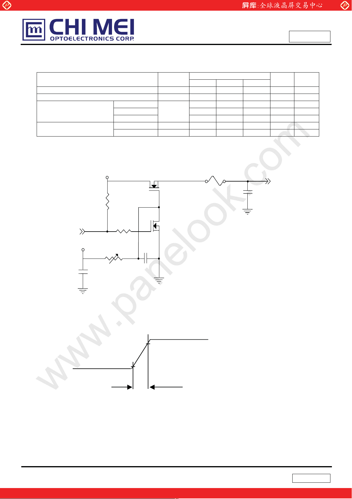
a. White Pattern
c. Vertical Stripe Pattern
= 60 Hz, whereas a power dissipation check pattern below is displayed.
v
b. Black Pattern
Active Area
Active Area
R
R
B
R
B
G
G
G
B
B
B
R
R
R
G
G
G
B
B
B
R
R
Active Area
R R
G
B
G
B
3.2 BACKLIGHT UNIT Ta = 25 r 2 ºC
Parameter Symbol
Lamp Input Voltage VL 603 670 737 V
Lamp Current IL 2.0 5.5 6.5 mA
Lamp Turn On Voltage VS
Operating Frequency FL 30 45 80 KHz (3)
Lamp Life Time LBL 40,000 50,000 - Hrs (5)
Power Consumption PL - 14,740 - mW (4), IL = 5.5 mA
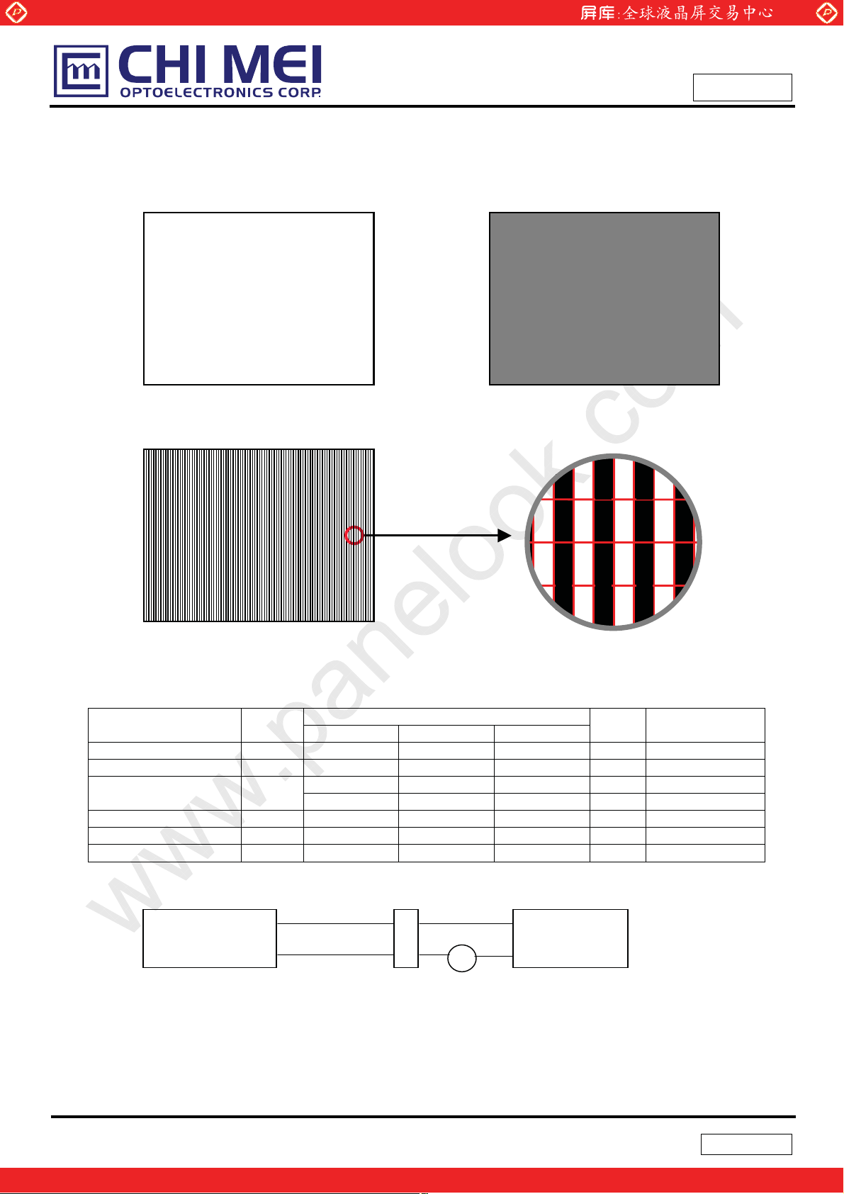
Note (1) Lamp current is measured by utilizing a high frequency current meter as shown below:
LCD
Module
HV (Pink/ Blue)
LV (White/ Black)
Min. Typ. Max.
- - 870 (25
- - 1,090 (0
Value
1
2
Current Meter
Unit Note
o
C) V
o
C) V
I
RMS
(1)
RMS
(2)
RMS
(2)
RMS
= 5.5mA
L
Inverter
A
Note (2) The voltage shown above should be applied to the lamp for more than 1 second after startup.
Otherwise the lamp may not be turned on.
9 / 25
One step solution for LCD / PDP / OLED panel application: Datasheet, inventory and accessory!
Version 3.1
www.panelook.com
Page 10

Global LCD Panel Exchange Center
Note (3) The lamp frequency may generate interference with horizontal synchronous frequency from the
display, and this may cause line flow on the display. In order to avoid interference, the lamp
frequency should be detached from the horizontal synchronous frequency and its harmonics as far
as possible.
www.panelook.com
Issued Date:Jan.15’2003
Model No.: M150X3-T03
Approval
Note (4) P
Note (5) The lifetime of lamp is defined as the time when it continues to operate under the conditions at Ta
Note (6) The waveform of the voltage output of inverter must be area-symmetric and the design of the
= IL X VL
L
= 25 r2
(a) When the brightness becomes d 50% of its original value.
(b) When the effective ignition length becomes d 80% of its original value. (Effective ignition length
inverter must have specifications for the modularized lamp. The performance of the Backlight,
such as lifetime or brightness, is greatly influenced by the characteristics of the DC-AC inverter for
the lamp. All the parameters of an inverter should be carefully designed to avoid generating too
much current leakage from high voltage output of the inverter. When designing or ordering the
inverter please make sure that a poor lighting caused by the mismatch of the Backlight and the
inverter (miss-lighting, flicker, etc.) never occurs. If the above situation is confirmed, the module
should be operated in the same manners when it is installed in your instrument.
o
C and IL =6.5mA
is defined as an area that the brightness is less than 70% compared to the center point.)
until one of the following events occurs:
RMS
10 / 25
One step solution for LCD / PDP / OLED panel application: Datasheet, inventory and accessory!
Version 3.1
www.panelook.com
Page 11

Global LCD Panel Exchange Center
)
)
)
)
)
)
)
)
4. BLOCK DIAGRAM
4.1 TFT LCD MODULE
www.panelook.com
Issued Date:Jan.15’2003
Model No.: M150X3-T03
Approval
ENAB
DCLK
GND
V
DD
RO0~RO5
GO0~GO5
BO0~BO5
RE0~RE5
GE0~GE5
BE0~BE5
(M0lex 52760-0600)
LAMP CONNECTOR
4.2 BACKLIGHT UNIT
INPUT CONNECTOR
REFERENCE VOLTAGE
(JST-BHSR-02VS-1)
TTL INPUT /
TIMING CONTROLLER
DC/DC CONVERTER &
GENERATOR
SCAN DRIVER IC
TFT LCD PANEL
(1024x3x768)
DATA DRIVER IC
BACKLIGHT UNIT
1 HV (Pink/ Blue
2 LV (White/ Black
1 HV (Pink/ Blue
2 LV (White/ Black
1 HV (Pink/ Blue
2 LV (White/ Black
1 HV (Pink/ Blue
2 LV (White/ Black
11 / 25
One step solution for LCD / PDP / OLED panel application: Datasheet, inventory and accessory!
Version 3.1
www.panelook.com
Page 12

Global LCD Panel Exchange Center
5. INPUT TERMINAL PIN ASSIGNMENT
5.1 TFT LCD MODULE
Pin
No.
1 GND - Ground 31 GE1 I Green even data 1
2 RO0 I Red odd data 0 32 GE2 I Green even data 2
3 RO1 I Red odd data 1 33 GE3 I Green even data 3
4 RO2 I Red odd data 2 34 GE4 I Green even data 4
5 RO3 I Red odd data 3 35 GE5 I Green even data 5
6 RO4 I Red odd data 4 36 GND - Ground
7 RO5 I Red odd data 5 37 BE0 I Blue even data 0
8 GND - Ground 38 BE1 I Blue even data 1
9 GO0 I Green odd data 0 39 BE2 I Blue even data 2
10 GO1 I Green odd data 1 40 BE3 I Blue even data 3
11 GO2 I Green odd data 2 41 BE4 I Blue even data 4
12 GO3 I Green odd data 3 42 BE5 I Blue even data 5
13 GO4 I Green odd data 4 43 GND - Ground
14 GO5 I Green odd data 5 44 PULL I Must be fixed to 0 V
15 GND - Ground 45 PULL I Must be fixed to 0 V
16 BO0 I Blue odd data 0 46 ENAB I Data enable signal
17 BO1 I Blue odd data 1 47 GND - Ground
18 BO2 I Blue odd data 2 48 GND - Ground
19 BO3 I Blue odd data 3 49 DCLK I Dot clock signal
20 BO4 I Blue odd data 4 50 GND - Ground
21 BO5 I Blue odd data 5 51 GND - Ground
22 GND - Ground 52 NC - Must be floating
23 RE0 I Red even data 0 53 NC - Must be floating
24 RE1 I Red even data 1 54 GND - Ground
25 RE2 I Red even data 2 55 GND - Ground
26 RE3 I Red even data 3 56 GND - Ground
27 RE4 I Red even data 4 57 VDD - +3.3V Power supply
28 RE5 I Red even data 5 58 VDD - +3.3V Power supply
29 GND - Ground 59 VDD - +3.3V Power supply
30 GE0 I Green even data 0 60 VDD - +3.3V Power supply
Connector Part No.: 52760-0600(Molex)
Symbol I/O Function Pin
www.panelook.com
Issued Date:Jan.15’2003
Model No.: M150X3-T03
Approval
Symbol I/O Function
No.
User’s connector Part No: 53475-0600(Molex)
12 / 25
One step solution for LCD / PDP / OLED panel application: Datasheet, inventory and accessory!
Version 3.1
www.panelook.com
Page 13

Global LCD Panel Exchange Center
www.panelook.com
Issued Date:Jan.15’2003
Model No.: M150X3-T03
Correspondence between Data and Display Position
S0001 S0002 S0003 S0004 S0005 S0006 S0007 S0008 S3071 S3072
C001 RE
0001
C768 RE
0001
GE
0001
GE
0001
BE
0001
BE
0001
RO
0002
RO
0002
GO
0002
GO
0002
BO
0002
BO
0002
RE
0003
RE
0003
GE
0003
GE
0003
GO
1024
GO
1024
BO
1024
BO
1024
Approval
5.2 BACKLIGHT UNIT
Pin Symbol Description Color
1 HV1 High Voltage Pink/ Blue
2 LV Ground White/ Black
Note (1) Connector Part No.: BHSR-02VS-1 (JST) or equivalent
Note (2) Matching Connector Part No.: SM02B-BHS-1-TB (JST) or equivalent
13 / 25
One step solution for LCD / PDP / OLED panel application: Datasheet, inventory and accessory!
Version 3.1
www.panelook.com
Page 14

Global LCD Panel Exchange Center
5.3 COLOR DATA INPUT ASSIGNMENT
The brightness of each primary color (red, green and blue) is based on the 6-bit gray scale data input for
the color. The higher the binary input the brighter the color. The table below provides the assignment of
color versus data input.
Basic
Colors
Gray
Scale
Of
Red
Gray
Scale
Of
Green
Gray
Scale
Of
Blue
Color
R5 R4 R3 R2 R1 R0 G5 G4 G3 G2 G1 G0 B5 B4 B3 B2 B1 B0
Black
Red
Green
Blue
Cyan
Magenta
Ye ll ow
White
Red(0) / Dark
Red(1)
Red(2)
:
:
Red(61)
Red(62)
Red(63)
Green(0) / Dark
Green(1)
Green(2)
:
:
Green(61)
Green(62)
Green(63)
Blue(0) / Dark
Blue(1)
Blue(2)
:
:
Blue(61)
Blue(62)
Blue(63)
Note (1) 0: Low Level Voltage, 1: High Level Voltage
0
1
0
0
0
1
1
1
0
0
0
:
:
1
1
1
0
0
0
:
:
0
0
0
0
0
0
:
:
0
0
0
www.panelook.com
Issued Date:Jan.15’2003
Model No.: M150X3-T03
Approval
Data Signal
Red Green Blue
0
0
0
0
0
0
0
0
0
0
0
0
0
0
0
0
0
1
1
1
1
1
0
0
0
0
0
0
0
0
0
0
0
0
0
0
0
0
0
1
1
1
1
1
1
0
0
0
0
0
0
0
0
0
0
0
0
0
0
0
0
0
1
1
1
1
1
1
0
0
0
0
0
1
1
1
1
1
1
1
1
1
1
1
1
1
1
1
1
1
0
0
0
0
0
0
1
1
1
1
1
1
1
1
1
1
1
1
1
1
1
1
1
0
0
0
0
0
0
1
1
1
1
1
1
1
1
1
1
1
1
1
1
1
1
1
0
0
0
0
0
0
0
0
0
0
0
0
0
0
0
0
0
0
0
0
0
1
0
0
0
0
0
0
0
0
0
0
0
0
0
0
0
1
0
0
0
0
0
0
0
0
0
0
0
0
0
:
:
:
:
:
:
:
:
:
:
:
:
:
:
:
:
:
:
:
:
:
:
:
:
:
:
:
:
:
:
:
:
:
:
1
1
1
0
1
0
0
0
0
0
0
0
0
0
0
0
0
1
1
1
1
0
0
0
0
0
0
0
0
0
0
0
0
0
1
1
1
1
1
0
0
0
0
0
0
0
0
0
0
0
0
0
0
0
0
0
0
0
0
0
0
0
0
0
0
0
0
0
0
0
0
0
0
0
0
0
0
0
1
0
0
0
0
0
0
0
0
0
0
0
0
0
0
0
1
0
0
0
0
0
0
0
:
:
:
:
:
:
:
:
:
:
:
:
:
:
:
:
:
:
:
:
:
:
:
:
:
:
:
:
:
:
:
:
:
:
0
0
0
0
0
1
1
1
1
0
1
0
0
0
0
0
0
0
0
0
0
0
1
1
1
1
1
0
0
0
0
0
0
0
0
0
0
0
0
1
1
1
1
1
1
0
0
0
0
0
0
0
0
0
0
0
0
0
0
0
0
0
0
0
0
0
0
0
0
0
0
0
0
0
0
0
0
0
0
0
0
0
0
0
1
0
0
0
0
0
0
0
0
0
0
0
0
0
0
0
1
0
:
:
:
:
:
:
:
:
:
:
:
:
:
:
:
:
:
:
:
:
:
:
:
:
:
:
:
:
:
:
:
:
:
:
0
0
0
0
0
0
0
0
0
0
0
1
1
1
1
0
1
0
0
0
0
0
0
0
0
0
0
0
1
1
1
1
1
0
0
0
0
0
0
0
0
0
0
0
0
1
1
1
1
1
1
14 / 25
One step solution for LCD / PDP / OLED panel application: Datasheet, inventory and accessory!
Version 3.1
www.panelook.com
Page 15

Global LCD Panel Exchange Center
6. INTERFACE TIMING
6.1 INPUT SIGNAL TIMING SPECIFICATIONS
The input signal timing specifications are shown as the following table and timing diagram.
Signal Parameter Symbol Min Typ Max Unit Remarks
DCLK
Ver t i c al
Signal
Horizontal
Signal
Pixel clock Frequency Fck - 32.5 40 MHz
Pixel clock period Tck 25 30 40 ns
Duty ratio (%Tch) - 45 50 55 % Tch/Tck
High time Tckh 5 - - ns
Low time Tckl 5 - - ns
Setup time Tsd 4 - - ns DATA
Hold time Thd 4 - - ns
Setup time Tsde 4 - - ns DE
Hold time Thde 4 - - ns
Vertical Frequency Fv - 60 75 Hz
Vertical display active period Tvda 768 768 768 Thp
Vertical display blank period Tvdb 1 38 - Thp
Vertical period Tvp 769 806 - Thp
Horizontal display active
period
Horizontal display blank period Thdb 38 160 388 Tck
Horizontal period Thp 550 672 900 Tck
www.panelook.com
Thda 512 512 512 Tck
Issued Date:Jan.15’2003
Model No.: M150X3-T03
Approval
Note (1) Because this module is operated by DE only mode, Hsync and Vsync input signals should be set
to low logic level or ground. Otherwise, this module would operate abnormally.
15 / 25
One step solution for LCD / PDP / OLED panel application: Datasheet, inventory and accessory!
Version 3.1
www.panelook.com
Page 16

Global LCD Panel Exchange Center
DE
DE
768
www.panelook.com
INPUT SIGNAL TIMING DIAGRAM
Tvp
Thp
Tvda
2
Thda
768
Tvdb
1
Thdb
Issued Date:Jan.15’2003
Model No.: M150X3-T03
Approval
DCLK
DATA
DCLK
DATA
DE
Tck hr
Valid display data (1024 Tck)
Tck l
Tch
Tsde
Invalid Va l i d
Tck
0.3VDD
Thd Tsd
0.7VDD
0.3VDD
Thde
16 / 25
One step solution for LCD / PDP / OLED panel application: Datasheet, inventory and accessory!
Version 3.1
www.panelook.com
Page 17

Global LCD Panel Exchange Center
6.2 POWER ON/OFF SEQUENCE
Power On
90%
www.panelook.com
Power Off
90%
Issued Date:Jan.15’2003
Model No.: M150X3-T03
Approval
Restart
t4
Power Supply
for LCD, VDD
- Interface Signal
(LVDS Signal of
Transmitter), V
0V
0V
I
10%
t1
Valid Data
t6 t5
10%
t3 t2
10%
- Power for Lamp
ONOFF OFF
Timing Specifications:
0 < t1 d 10 msec
0 < t2 d 50 msec
0 < t3 d 50 msec
t4 t 1 sec
t5 t 100 mesc
t6 t 100 msec
Note (1) Please avoid floating state of interface signal at invalid period.
Note (2) When the interface signal is invalid, be sure to pull down the power supply of LCD V
to 0 V.
DD
Note (3) The Backlight inverter power must be turned on after the power supply for the logic and the
interface signal is valid. The Backlight inverter power must be turned off before the power supply
for the logic and the interface signal is invalid.
17 / 25
Version 3.1
One step solution for LCD / PDP / OLED panel application: Datasheet, inventory and accessory!
www.panelook.com
Page 18

Global LCD Panel Exchange Center
7. OPTICAL CHARACTERISTICS
7.1 TEST CONDITIONS
Item Symbol Value Unit
Ambient Temperature Ta
Ambient Humidity Ha
Supply Voltage VDD 3.3 V
Input Signal According to typical value in "3. ELECTRICAL CHARACTERISTICS"
Inverter Current IL 5.5 mA
The measurement methods of optical characteristics are shown in Section 7.2. The following items
should be measured under the test conditions described in Section 7.1 and stable environment shown in
Note (4).
7.2 OPTICAL SPECIFICATIONS
Item Symbol Condition Min. Typ. Max. Unit Note
Contrast Ratio CR 250
Response Time
Center Luminance of White L 200 300 - cd/m
Red
Color
Chromaticity
Viewing Angle
Green
Blue
White
Horizontal
Ver t i c al
www.panelook.com
Issued Date:Jan.15’2003
Model No.: M150X3-T03
Approval
o
25r2
50r10
300
TR -
-
T
F
7
23
- - (2), (4)
22 ms
38 ms
Rx 0.607 0.637 0.667 Ry 0.323 0.353 0.383 Gx 0.272 0.302 0.332 -
=0q, TY =0q
T
x
Viewing Normal Angle
Gy 0.558 0.588 0.618 -
Bx 0.111 0.141 0.171 -
By 0.064 0.094 0.124 Wx 0.280 0.310 0.340 Wy
Tx+
T
x
TY+
T
Y
CRt10
-
0.300 0.330 0.360 50 60 50 60 30 40 50 60 -
C
%RH
Deg.
2
(3)
(4)
(1), (4)
18 / 25
Version 3.1
One step solution for LCD / PDP / OLED panel application: Datasheet, inventory and accessory!
www.panelook.com
Page 19

Global LCD Panel Exchange Center
T
Note (1) Definition of Viewing Angle (Tx, Ty):
www.panelook.com
Issued Date:Jan.15’2003
Model No.: M150X3-T03
Approval
TX- = 90º
x-
6 o’clock
T
y- = 90º
y-
Note (2) Definition of Contrast Ratio (CR):
The contrast ratio can be calculated by the following expression.
Normal
Tx = Ty = 0º
Ty- Ty
Tx-
Tx
12 o’clock direction
y+
T
y+ = 90º
x+
TX+ = 90º
Contrast Ratio (CR) = L63 / L0
L63: Luminance of gray level 63
L 0: Luminance of gray level 0
CR = CR (5)
CR (X) is corresponding to the Contrast Ratio of the point X at Figure in Note (5).
Note (3) Definition of Response Time (T
100%
90%
Optical
Response
Gray Level 63
10%
0%
, TF):
R
Gray Level 63
Gray Level 0
ime
T
R
T
F
19 / 25
One step solution for LCD / PDP / OLED panel application: Datasheet, inventory and accessory!
Version 3.1
www.panelook.com
Page 20

Global LCD Panel Exchange Center
Note (4) Measurement Setup:
The LCD module should be stabilized at given temperature for 20 minutes to avoid abrupt
temperature change during measuring. In order to stabilize the luminance, the measurement
should be executed after lighting Backlight for 20 minutes in a windless room.
LCD Module
www.panelook.com
Issued Date:Jan.15’2003
Model No.: M150X3-T03
Approval
Note (5) Definition of luminance measured points:
LCD Panel
Center of the Screen
Field of View = 2º
500 mm
0
Horizontal Line Number
256 512 768 1023
0
Photometer
(TOPCON BM-5A)
Light Shield Room
(Ambient Luminance < 2 lux)
192
384
1
5
576
3
2
: test point
X
X=1 to 5
4
Vertical Line Number
767
Active area
One step solution for LCD / PDP / OLED panel application: Datasheet, inventory and accessory!
Horizontal Line Number [pixel]
20 / 25
Version 3.1
www.panelook.com
Page 21

Global LCD Panel Exchange Center
8. PRECAUTIONS
8.1 HANDLING PRECAUTIONS
(1) The module should be assembled into the system firmly by using every mounting hole. Be careful not
to twist or bend the module.
(2) While assembling or installing modules, it can only be in the clean area. The dust and oil may cause
electrical short or damage the polarizer.
(3) Use fingerstalls or soft gloves in order to keep display clean during the incoming inspection and
assembly process.
(4) Do not press or scratch the surface harder than a HB pencil lead on the panel because the polarizer is
very soft and easily scratched.
(5) If the surface of the polarizer is dirty, please clean it by some absorbent cotton or soft cloth. Do not use
Ketone type materials (ex. Acetone), Ethyl alcohol, Toluene, Ethyl acid or Methyl chloride. It might
www.panelook.com
Issued Date:Jan.15’2003
Model No.: M150X3-T03
Approval
permanently damage the polarizer due to chemical reaction.
(6) Wipe off water droplets or oil immediately. Staining and discoloration may occur if they left on panel for
a long time.
(7) If the liquid crystal material leaks from the panel, it should be kept away from the eyes or mouth. In
case of contacting with hands, legs or clothes, it must be washed away thoroughly with soap.
(8) Protect the module from static electricity, it may cause damage to the C-MOS Gate Array IC.
(9) Do not disassemble the module.
(10) Do not pull or fold the lamp wire.
(11) Pins of I/F connector should not be touched directly with bare hands.
8.2 STORAGE PRECAUTIONS
(1) High temperature or humidity may reduce the performance of module. Please store LCD module within
the specified storage conditions.
(2) It is dangerous that moisture come into or contacted the LCD module, because the moisture may
damage LCD module when it is operating.
(3) It may reduce the display quality if the ambient temperature is lower than 10 ºC. For example, the
response time will become slowly, and the starting voltage of lamp will be higher than the room
temperature.
8.3 OPERATION PRECAUTIONS
(1) Do not pull the I/F connector in or out while the module is operating.
(2) Always follow the correct power on/off sequence when LCD module is connecting and operating. This
can prevent the CMOS LSI chips from damage during latch-up.
(3) The startup voltage of Backlight is approximately 1000 Volts. It may cause electrical shock while
assembling with inverter. Do not disassemble the module or insert anything into the Backlight unit.
21 / 25
One step solution for LCD / PDP / OLED panel application: Datasheet, inventory and accessory!
Version 3.1
www.panelook.com
Page 22

Global LCD Panel Exchange Center
9. PACKAGING
9.1 PACKING SPECIFICATIONS
(1) 5 LCD modules / 1 Box
(2) Box dimensions : 353(L) X 268(W) X 462(H) mm
www.panelook.com
Issued Date:Jan.15’2003
Model No.: M150X3-T03
Approval
(3) Weight : approximately 8.5Kg ( 5 modules per box)
9.2 PACKING Method
Figures 9-1and 9-2 are the packing method.
Figure. 9-1 Packing method
22 / 25
One step solution for LCD / PDP / OLED panel application: Datasheet, inventory and accessory!
Version 3.1
www.panelook.com
Page 23

Global LCD Panel Exchange Center
www.panelook.com
Issued Date:Jan.15’2003
Model No.: M150X3-T03
Approval
Figure. 9-2 Packing method
23 / 25
One step solution for LCD / PDP / OLED panel application: Datasheet, inventory and accessory!
Version 3.1
www.panelook.com
Page 24

Global LCD Panel Exchange Center
www.panelook.com
Issued Date:Jan.15’2003
Model No.: M150X3-T03
Approval
10. INCOMING INSPECTION DAY
The Supplier should be acquainted the inspection results (acceptance or rejection) by Customer, and the results
are in accordance with the incoming inspection standard within 30 days after the date of the bills of lading.
Should Customer fail to so notify the Supplier within the said 30 days period. The Customer’s right to reject the
LCMS shall then lapse, and the said LCMS shall be deemed to have been accepted by the customer.
24 / 25
One step solution for LCD / PDP / OLED panel application: Datasheet, inventory and accessory!
Version 3.1
www.panelook.com
Page 25

Global LCD Panel Exchange Center
11. DEFINITION OF LABELS
11.1 CMO MODULE LABEL
The barcode nameplate is pasted on each module as illustration, and its definitions are as following
explanation.
M150X3 -T03 Rev. XX
CHI MEI
OPTOELECTRONICS
(a) Model Name: M150X3 –T03
(b) Revision: Rev. XX, for example: C1, C2 …etc.
www.panelook.com
MADE IN TAIWAN
X X X X X X X Y M D L N N N N
Issued Date:Jan.15’2003
Model No.: M150X3-T03
Approval
E207943
MADE IN TAIWAN
(c) Serial ID: X X
Serial ID includes the information as below:
(a) Manufactured Date: Year: 1~9, for 2000~2009
Day: 1~9, A~Y, for 1
(b) Revision Code: cover all the change
(c) Color Filter: 0 ->CMO, 2 -> Toppan
X X X X X Y M D L N N N N
Month: 1~9, A~C, for Jan. ~ Dec.
Serial No.
Product Line
Year, Month, Date
CMO Internal Use
Color Filter
Revision
CMO Internal Use
st
to 31st, exclude I and O
(d) Serial No.: Manufacturing sequence of product
(e) Product Line: 1 -> Line1, 2 -> Line 2, …etc.
25 / 25
One step solution for LCD / PDP / OLED panel application: Datasheet, inventory and accessory!
Version 3.1
www.panelook.com
Page 26

www.panelook.com
www.panelook.com
Global LCD Panel Exchange Center
One step solution for LCD / PDP / OLED panel application: Datasheet, inventory and accessory!
Page 27

www.panelook.com
E207943
MADE IN TAIWAN
M150X3 Rev. C1-T03
CAUTION
HIGH VOLTAGE
RISK OF ELECTRIC SHOCK.
DISCONNECT THE ELECTRIC
POWER BEFORE SERVICING.
COLD CATHODE FLUORESCENT LAMP IN LCD PANEL CONTAINS A SMALL AMOUNT OF
MERCURY PLEASE FOLLOW LOCAL ORDINANCES OR REGULATIONS FOR DISPOSAL.
www.panelook.com
Global LCD Panel Exchange Center
One step solution for LCD / PDP / OLED panel application: Datasheet, inventory and accessory!
 Loading...