

Page 1
Global LCD Panel Exchange Center
ுழၴ
ຝ
ᐉு
ߡۥ
ދป
TFT LCD Approval Specification
MODEL NO.: G121X1-L01
www.panelook.com
Issued Date: Aug. 23, 2010
Model No.: G121X1-L01
Approval
Customer:
Approved by:
Note:
2010-09-09
16:32:42 ʳ
Version 3.3
One step solution for LCD / PDP / OLED panel application: Datasheet, inventory and accessory!
ʳ
ʳ
APPL
ขጥʳ
്ʳ
1 / 27
ʳ
ʳ
Directorʳ Acceptʳ
ʳ
www.panelook.com
Page 2
Global LCD Panel Exchange Center
www.panelook.com
Issued Date: Aug. 23, 2010
Model No.: G121X1-L01
Approval
- CONTENTS -
REVISION HISTORY ------------------------------------------------------- 3
1. GENERAL DESCRIPTION
1.1 OVERVIEW
1.2 FEATURES
1.3 APPLICATION
1.4 GENERAL SPECIFICATIONS
1.5 MECHANICAL SPECIFICATIONS
------------------------------------------------------- 4
2. ABSOLUTE MAXIMUM RATINGS ------------------------------------------------------- 6
2.1 ABSOLUTE RATINGS OF ENVIRONMENT
2.2 ELECTRICAL ABSOLUTE RATINGS
2.2.1 TFT LCD MODULE
2.2.2 BACKLIGHT UNIT
3. ELECTRICAL CHARACTERISTICS ------------------------------------------------------- 8
3.1 TFT LCD MODULE
3.2 BACKLIGHT UNIT
4. BLOCK DIAGRAM ------------------------------------------------------- 12
4.1 TFT LCD MODULE
4.2 BACKLIGHT UNIT
5. INPUT TERMINAL PIN ASSIGNMENT ------------------------------------------------------- 13
5.1 TFT LCD MODULE
5.2 BACKLIGHT UNIT
5.3 TIMING DIAGRAM OF LVDS INPUT SIGNAL
5.4 COLOR DATA INPUT ASSIGNMENT
6. INTERFACE TIMING ------------------------------------------------------- 15
6.1 INPUT SIGNAL TIMING SPECIFICATIONS
6.2 POWER ON/OFF SEQUENCE
7. OPTICAL CHARACTERISTICS
7.1 TEST CONDITIONS
7.2 OPTICAL SPECIFICATIONS
------------------------------------------------------- 17
8. RELIABILITY TEST CRIRERIA ------------------------------------------------------- 21
9. PACKAGING
9.1 PACKING SPECIFICATIONS
9.2 PACKING METHOD
------------------------------------------------------- 22
10. DEFINITION OF LABELS ------------------------------------------------------- 24
11. PRECAUTIONS
11.1 ASSEMBLY AND HANDLING PRECAUTIONS
11.2 SAFETY PRECAUTIONS
12. MECHANICAL CHARACTERISTICS
------------------------------------------------------- 25
------------------------------------------------------- 26
2 / 27
Version 3.3
One step solution for LCD / PDP / OLED panel application: Datasheet, inventory and accessory!
www.panelook.com
Page 3
Global LCD Panel Exchange Center
www.panelook.com
REVISION HISTORY
Version Date Section Description
G121X1-L01 Approval Specification was first issued.
Ver. 3.0
Sep.12, ’06
All
Issued Date: Aug. 23, 2010
Model No.: G121X1-L01
Approval
Ver. 3.1
Ver. 3.2
Ver. 3.3
Nov. 9, ’06
Aug. 26, ’08
Aug. 23, ‘10
Outline
3.2
7.2
10.1
3.2
8
Added connector pin number.
Modify Backlight Unit Note (5) statement.
Modify Optical Specification measurement setup figure.
Add precaution of “Image sticking” in section 10.1 Assembly and handling
precaution: (11) Do not keep same pattern in a long period of time. It may cause
image sticking on LCD.
Add cautionary statement to Note(5) about life time vs. operating conditions.
Split reliability test criteria from 2.1 to Chapter 8.
3 / 27
Version 3.3
One step solution for LCD / PDP / OLED panel application: Datasheet, inventory and accessory!
www.panelook.com
Page 4
Global LCD Panel Exchange Center
1. GENERAL DESCRIPTION
1.1 OVERVIEW
The G121X1-L01 model is a 12.1” TFT-LCD module with a 2-CCFL Backlight Unit and a 20-pin
1ch-LVDS interface. This module supports 1024 x 768 XGA mode and displays 262,144 colors. The
inverter module for the Backlight Unit is not built in.
1.2 FEATURES
- Wide viewing angle
- High contrast ratio
- Fast response time
- High color saturation
- XGA (1024 x 768 pixels) resolution
www.panelook.com
Issued Date: Aug. 23, 2010
Model No.: G121X1-L01
Approval
- Wide operating temperature
- DE (Data Enable) mode
- LVDS (Low Voltage Differential Signaling) interface
- RoHS Compliance
1.3 APPLICATION
- TFT LCD Monitor
- TFT LCD TV
- Factory Application
- Amusement
- Vehicle
1.4 GENERAL SPECIFICATI0NS
Item Specification Unit Note
Diagonal Size 12.1 inch
Active Area 245.76(H) x 184.32(V) mm
Bezel Opening Area 249.00(H) x 187.50(V) mm
Driver Element a-si TFT active matrix - Pixel Number 1024 x R.G.B. x 768 pixel Pixel Pitch 0.240(H) x 0.240(V) mm Pixel Arrangement RGB vertical stripe - Display Colors 262,144 color Transmissive Mode Normally white - Surface Treatment Hard coating (3H), Anti-glare (Haze 25%) - -
(1)
4 / 27
Version 3.3
One step solution for LCD / PDP / OLED panel application: Datasheet, inventory and accessory!
www.panelook.com
Page 5
Global LCD Panel Exchange Center
1.5 MECHANICAL SPECIFICATIONS
Item Min. Typ. Max. Unit Note
Horizontal (H) 260.0 260.5 261.0 mm
Module Size
I/F connector mounting
Note (1) Please refer to the attached drawings for more information of front and back outline dimensions.
(2) Connector mounting position
Vertical (V) 203.5 204.0 204.5 mm
Depth (D) 11.7 12.2 12.7 mm
Weight - - 660 g -
position
www.panelook.com
The mounting inclination of the connector makes
the screen center within ±0.5mm as the horizontal.
+/- 0.5mm
Issued Date: Aug. 23, 2010
Model No.: G121X1-L01
Approval
(1)
-
(2)
5 / 27
Version 3.3
One step solution for LCD / PDP / OLED panel application: Datasheet, inventory and accessory!
www.panelook.com
Page 6
Global LCD Panel Exchange Center
2. ABSOLUTE MAXIMUM RATINGS
2.1 ABSOLUTE RATINGS OF ENVIRONMENT
Item Symbol
Operating Ambient Temperature TOP -30 +70 ºC (1), (2)
Storage Temperature TST -40 +80 ºC (1)
Note (1) Temperature and relative humidity range is shown in the figure below.
(a) 90 %RH Max. (Ta Љ 40 ºC).
(b) Wet-bulb temperature should be 39 ºC Max. (Ta > 40 ºC).
(c) No condensation.
www.panelook.com
Value
Min. Max.
Issued Date: Aug. 23, 2010
Model No.: G121X1-L01
Approval
Unit Note
Note (2) No display malfunctions.
6 / 27
Version 3.3
One step solution for LCD / PDP / OLED panel application: Datasheet, inventory and accessory!
www.panelook.com
Page 7
Global LCD Panel Exchange Center
2.2 ELECTRICAL ABSOLUTE RATINGS
2.2.1 TFT LCD MODULE
Item Symbol
Power Supply Voltage Vcc -0.3 4.0 V
Logic Input Voltage VIN -0.3 2.7 V
2.2.2 BACKLIGHT UNIT
Item Symbol
Lamp Voltage VL - 2.5K V
Lamp Current IL 2.0 8.5 mA
Lamp Frequency FL 45 80 KHz
Note (1) Permanent damage to the device may occur if maximum values are exceeded. Function
operation should be restricted to the conditions described under Normal Operating Conditions.
www.panelook.com
Value
Min. Max.
Value
Min. Max.
Unit Note
Unit Note
Issued Date: Aug. 23, 2010
Model No.: G121X1-L01
Approval
(1)
(1), (2), IL = (8)mA
RMS
RMS
(1), (2)
Note (2) Specified values are for lamp (Refer to 3.2 for further information).
7 / 27
Version 3.3
One step solution for LCD / PDP / OLED panel application: Datasheet, inventory and accessory!
www.panelook.com
Page 8
Global LCD Panel Exchange Center
www.panelook.com
Issued Date: Aug. 23, 2010
Model No.: G121X1-L01
3. ELECTRICAL CHARACTERISTICS
3.1 TFT LCD MODULE Ta = 25 ± 2 ºC
Parameter Symbol
Min. Typ. Max.
Power Supply Voltage Vcc 3.0 3.3 3.6 V Ripple Voltage VRP - - 100 mV Rush Current I
Power Supply Current
White - 350 490 mA (3)a
Black
- - 1.0 A (2)
RUSH
-
- 510 650 mA (3)b
LVDS differential input voltage Vid -100 - +100 mV LVDS common input voltage Vic - 1.2 - V -
Note (1) The module is recommended to operate within specification ranges listed above for normal
function.
Note (2) Measurement Conditions:
Value
Unit Note
Approval
(High to Low)
(Control Signal)
SW
+12V
+3.3V
R1
47K
R2
1K
47K
VR1
C1
1uF
Q1 2SK1475
C2
0.01uF
Q2
2SK1470
FUSE
C3
1uF
Vcc
(LCD Module Input)
Vcc rising time is 470Ps
+3.3V
0.9Vcc
0.1Vcc
GND
470Ps
8 / 27
Version 3.3
One step solution for LCD / PDP / OLED panel application: Datasheet, inventory and accessory!
www.panelook.com
Page 9
Global LCD Panel Exchange Center
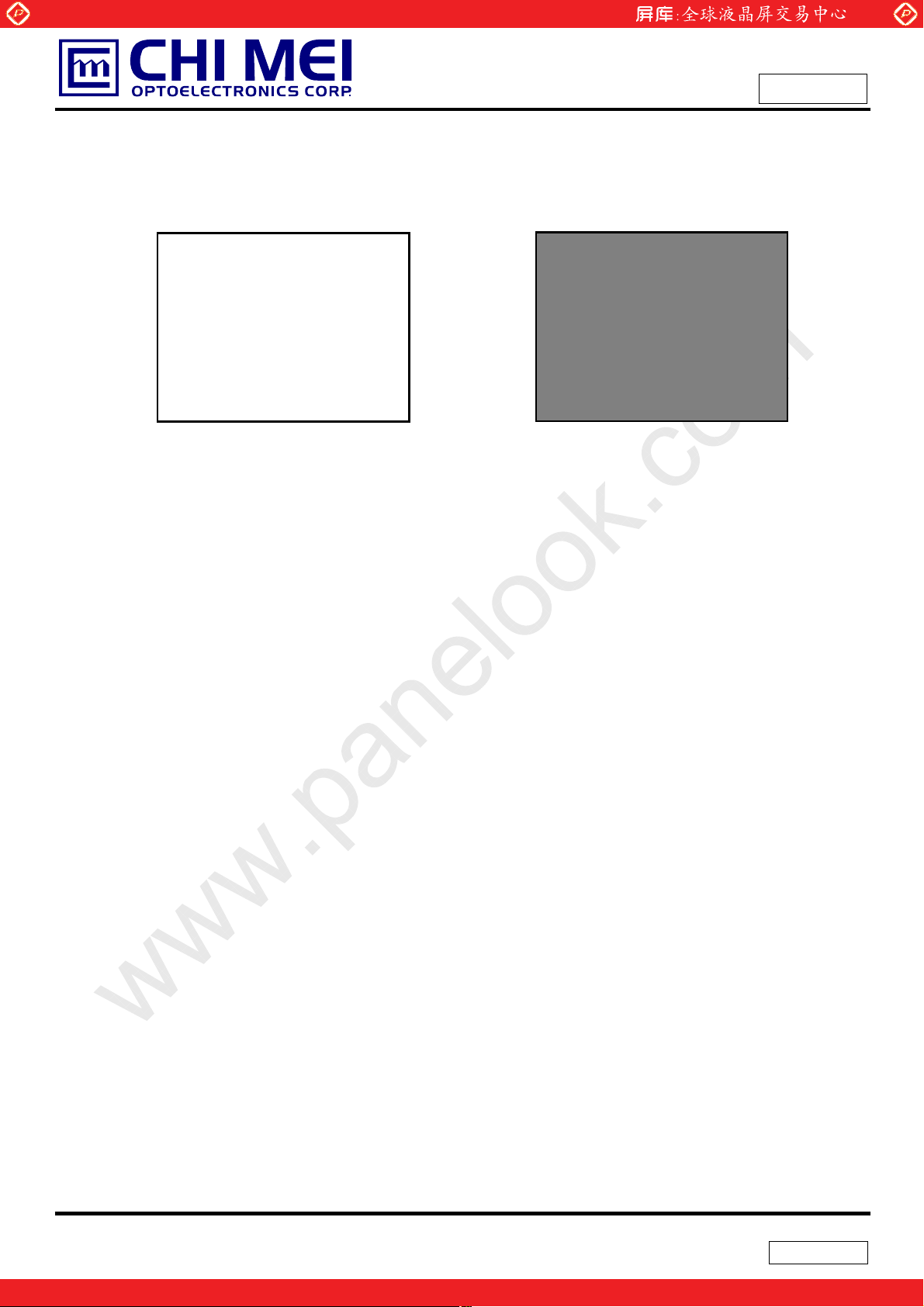
Note (3) The specified power supply current is under the conditions at Vcc = 3.3 V, Ta = 25 ± 2 ºC, fv = 60
Hz, whereas a power dissipation check pattern below is displayed.
www.panelook.com
Issued Date: Aug. 23, 2010
Model No.: G121X1-L01
Approval
a. White Pattern
Active Area
b. Black Pattern
Active Area
9 / 27
Version 3.3
One step solution for LCD / PDP / OLED panel application: Datasheet, inventory and accessory!
www.panelook.com
Page 10

Global LCD Panel Exchange Center
3.2 BACKLIGHT UNIT
Parameter Symbol
Lamp Input Voltage VL 423 470 517 V
Lamp Current IL 2.0 8.0 8.5 mA
Lamp Turn On Voltage V
Operating Frequency FL 45 - 80 KHz (3)
Lamp Life Time LBL 50000 - - Hrs (5), IL =8mA
Power Consumption PL - 3.76 - W (4), IL =8mA
Note (1) Lamp current is measured by utilizing high-frequency current meters as shown below:
S
www.panelook.com
Value
Min. Typ. Max.
- - 1010 V
- - 1200 V
Unit Note
RMS
RMS
RMS
Issued Date: Aug. 23, 2010
Model No.: G121X1-L01
Approval
I
(1)
RMS
25 ºC, (2)
0 ºC, (2)
=8mA
L
LCD
Module
HV (Pink)
LV (White)
HV (Pink)
LV (White)
1
2
A
Inverter
A
Current Meter
YOKOGAWA 2016
1
2
A
Ta = 25 ± 2 ºC
Note (2) The voltage that must be larger than Vs should be applied to the lamp for more than 1 second
after startup. Otherwise the lamp may not be turned on.
Note (3) The lamp frequency may produce interference with horizontal synchronization frequency from the
display, which might cause line flow on the display. In order to avoid interference, the lamp
frequency should be detached from the horizontal synchronization frequency and its harmonics
as far as possible.
Note (4) P
Note (5) The life time of lamp can be defined as the time in which it continues to operate under the
= I
L
LVL
condition Ta = 25 2
o
C and IL = 8.0 mArms until one of the following events occurs:
(a) When the brightness becomes or lower than 50% of its original value.
(b) When the effective ignition length becomesʳЉʳ80% of its original value. (The effective ignition
length is a scope that luminance is over 70% of that at the center point.)
Both life time and brightness are reduced if the lamp is operated under low temperature
environment. The life time of a lamp would also shorten when operated in portrait position or
cannot warm up adequately, e.g. turned ON/OFF frequently.
Note (6) The waveform of the voltage output of inverter must be area-symmetric and the design of the
inverter must have specifications for the modularized lamp. The performance of the Backlight,
such as lifetime or brightness, is greatly influenced by the characteristics of the DC-AC inverter
for the lamp. All the parameters of an inverter should be carefully designed to avoid producing too
much current leakage from high voltage output of the inverter. When designing or ordering the
inverter please make sure that a poor lighting caused by the mismatch of the Backlight and the
10 / 27
Version 3.3
One step solution for LCD / PDP / OLED panel application: Datasheet, inventory and accessory!
www.panelook.com
Page 11

Global LCD Panel Exchange Center
inverter (miss-lighting, flicker, etc.) never occurs. If the above situation is confirmed, the module
should be operated in the same manners when it is installed in your instrument.
The output of the inverter must have symmetrical (negative and positive) voltage waveform and
symmetrical current waveform. (Unsymmetrical ratio is less than 10%) Please do not use the inverter
which has unsymmetrical voltage and unsymmetrical current and spike wave. Lamp frequency may
produce interface with horizontal synchronous frequency and as a result this may cause beat on the
display. Therefore lamp frequency shall be as away possible from the horizontal synchronous
frequency and from its harmonics in order to prevent interference.
Requirements for a system inverter design, which is intended to have a better display performance, a
better power efficiency and a more reliable lamp. It shall help increase the lamp lifetime and reduce its
www.panelook.com
Issued Date: Aug. 23, 2010
Model No.: G121X1-L01
Approval
leakage current.
a. The asymmetry rate of the inverter waveform should be 10% below;
b. The distortion rate of the waveform should be within Ѕ2 ± 10%;
c. The ideal sine wave form shall be symmetric in positive and negative polarities.
* Asymmetry rate:
I p
I -p
| I
* Distortion rate
I
– I –p | / I
p
(or I –p) / I
p
rms
rms
* 100%
11 / 27
Version 3.3
One step solution for LCD / PDP / OLED panel application: Datasheet, inventory and accessory!
www.panelook.com
Page 12

Global LCD Panel Exchange Center
)
4. BLOCK DIAGRAM
4.1 TFT LCD MODULE
www.panelook.com
Issued Date: Aug. 23, 2010
Model No.: G121X1-L01
Approval
RX0(+/-)
RX1(+/-)
RX2(+/-)
RXC(+/-)
Vcc
GND
VL
(STARCONN 076B20-0048RA-G4
or JAE-FI-SEB20P-HFE
INPUT CONNECTOR
LAMP CONNECTOR
(JST BHR-03VS-1)
4.2 BACKLIGHT UNIT
LVDS INPUT /
TIMING CONTROLLER
DC/DC CONVERTER &
REFERENCE VOLTAGE
SCAN DRIVER IC
TFT LCD PANEL
(1024x R.G.B.x768)
DATA DRIVER IC
BACKLIGHT UNIT
1 HV(Pink)
1 HV(Pink)
2 LV(White)
2 LV(White)
12 / 27
Version 3.3
One step solution for LCD / PDP / OLED panel application: Datasheet, inventory and accessory!
www.panelook.com
Page 13

Global LCD Panel Exchange Center
5. INPUT TERMINAL PIN ASSIGNMENT
5.1 TFT LCD MODULE
Pin Name Description
1 VCC_IN Power Supply ( 3.3 V )
2 VCC_IN Power Supply ( 3.3 V )
3 GND Ground
4 GND Ground
5 RX0- Differential Data Input, CH0 (Negative )
6 RX0+ Differential Data Input, CH0 ( Positive )
7 GND Ground
8 RX1- Differential Data Input, CH1 ( Negative )
9 RX1+ Differential Data Input , CH1 ( Positive )
10 GND Ground
11 RX2- Differential Data Input , CH2 ( Negative )
12 RX2+ Differential Data Input , CH2 ( Positive )
13 GND Ground
14 CLK- Differential Clock Input ( Negative )
15 CLK+ Differential Clock Input ( Positive )
16 GND Ground
17 NA Non-connection
18 NA Non-connection
19 GND Ground
20 GND Ground
Note (1) Connector Part No.: STARCONN 076B20-0048RA-G4 or JAE FI-SEB20P-HFE or equivalent.
www.panelook.com
Issued Date: Aug. 23, 2010
Model No.: G121X1-L01
Approval
Remark
R0 ~ R5, G0
G1 ~ G5, B0, B1
B2 ~ B5, DE, Hsync, Vsync
LVDS Level Clock
Note (2) Mating Connector Part No.: JAE-FI-SE20M, FI-S20S or equivalent.
Note (3) The first pixel is odd.
Note (4) Input signal of even and odd clock should be the same timing.
13 / 27
Version 3.3
One step solution for LCD / PDP / OLED panel application: Datasheet, inventory and accessory!
www.panelook.com
Page 14
Global LCD Panel Exchange Center
5.2 BACKLIGHT UNIT
Pin Symbol Description Remark
1 HV High Voltage Pink
2 NA NA
3 LV Low Voltage White
Note (1) Connector Part No.: JST BHR-03VS-1 or equivalent
Note (2) User’s connector Part No.: JST SM03(4.0)B-BHS-1-TB or equivalent
5.3 COLOR DATA INPUT ASSIGNMENT
The brightness of each primary color (red, green and blue) is based on the 6-bit gray scale data input for
the color. The higher the binary input, the brighter the color. The table below provides the assignment of
color versus data input.
Color
R5 R4 R3 R2 R1 R0 G5 G4 G3 G2 G1 G0 B5 B4 B3 B2 B1 B0
Black
Red
Green
Basic
Colors
Gray
Scale
Of
Red
Gray
Scale
Of
Green
Gray
Scale
Of
Blue
Note (1) 0: Low Level Voltage, 1: High Level Voltage
Blue
Cyan
Magenta
Yellow
White
Red(0)/Dark
Red(1)
Red(2)
:
:
Red(61)
Red(62)
Red(63)
Green(0)/Dark
Green(1)
Green(2)
:
:
Green(61)
Green(62)
Green(63)
Blue(0)/Dark
Blue(1)
Blue(2)
:
:
Blue(61)
Blue(62)
Blue(63)
0
0
1
1
0
0
0
0
0
0
1
1
1
1
1
1
0
0
0
0
0
0
:
:
1
1
1
1
1
1
0
0
0
0
0
0
:
:
0
0
0
0
0
0
0
0
0
0
0
0
:
:
0
0
0
0
0
0
www.panelook.com
Issued Date: Aug. 23, 2010
Model No.: G121X1-L01
Approval
Data Signal
Red Green Blue
0
0
0
0
0
0
0
0
0
0
0
0
0
0
0
0
1
1
1
1
0
0
0
0
0
0
0
0
0
0
0
0
0
0
0
0
1
1
1
1
1
1
0
0
0
0
0
0
0
0
0
0
0
0
0
0
0
0
1
1
1
1
1
1
0
0
0
0
1
1
1
1
1
1
1
1
1
1
1
1
1
1
1
1
0
0
0
0
0
0
1
1
1
1
1
1
1
1
1
1
1
1
1
1
1
1
0
0
0
0
0
0
1
1
1
1
1
1
1
1
1
1
1
1
1
1
1
1
0
0
0
0
0
0
0
0
0
0
0
0
0
0
0
0
0
0
0
1
0
0
0
0
0
0
0
0
0
0
0
0
0
0
1
0
0
0
0
0
0
0
0
0
0
0
0
0
:
:
:
:
:
:
:
:
:
:
:
:
:
:
:
:
:
:
:
:
:
:
:
:
:
:
:
:
:
:
:
:
:
:
1
1
0
1
0
0
0
0
0
0
0
0
0
0
0
0
1
1
1
0
0
0
0
0
0
0
0
0
0
0
0
0
1
1
1
1
0
0
0
0
0
0
0
0
0
0
0
0
0
0
0
0
0
0
0
0
0
0
0
0
0
0
0
0
0
0
0
0
0
0
0
0
0
1
0
0
0
0
0
0
0
0
0
0
0
0
0
0
1
0
0
0
0
0
0
0
:
:
:
:
:
:
:
:
:
:
:
:
:
:
:
:
:
:
:
:
:
:
:
:
:
:
:
:
:
:
:
:
:
:
0
0
0
0
1
1
1
1
0
1
0
0
0
0
0
0
0
0
0
0
1
1
1
1
1
0
0
0
0
0
0
0
0
0
0
0
1
1
1
1
1
1
0
0
0
0
0
0
0
0
0
0
0
0
0
0
0
0
0
0
0
0
0
0
0
0
0
0
0
0
0
0
0
0
0
0
0
0
0
1
0
0
0
0
0
0
0
0
0
0
0
0
0
0
1
0
:
:
:
:
:
:
:
:
:
:
:
:
:
:
:
:
:
:
:
:
:
:
:
:
:
:
:
:
:
:
:
:
:
:
0
0
0
0
0
0
0
0
0
0
1
1
1
1
0
1
0
0
0
0
0
0
0
0
0
0
1
1
1
1
1
0
0
0
0
0
0
0
0
0
0
0
1
1
1
1
1
1
14 / 27
Version 3.3
One step solution for LCD / PDP / OLED panel application: Datasheet, inventory and accessory!
www.panelook.com
Page 15

Global LCD Panel Exchange Center
6. INTERFACE TIMING
6.1 INPUT SIGNAL TIMING SPECIFICATIONS
The input signal timing specifications are shown as the following table and timing diagram.
Signal Item Symbol Min. Typ. Max. Unit Note
DCLK
Vertical Active Display Term
Horizontal Active Display Term
NoteΚ(1) Because this module is operated by DE only mode, Hsync and Vsync input signals should be
set to low logic level or ground. Otherwise, this module would operate abnormally.
Frequency Fc 57.5 64.9 74.4 MHz
Period Tc 13.4 15.4 17.3 ns
Frame Rate Fr 56 60 75 Hz
Total Tv 774 806 848 Th Tv=Tvd+Tvb
Display Tvd 768 768 768 Th
Blank Tvb Tv-Tvd 38 Tv-Tvd Th
Total Th 1240 1344 1464 Tc Th=Thd+Thb
Display Thd 1024 1024 1024 Tc
Blank Thb Th-Thd 320 Th-Thd Tc
www.panelook.com
Issued Date: Aug. 23, 2010
Model No.: G121X1-L01
Approval
INPUT SIGNAL TIMING DIAGRAM
15 / 27
Version 3.3
One step solution for LCD / PDP / OLED panel application: Datasheet, inventory and accessory!
www.panelook.com
Page 16

Global LCD Panel Exchange Center
d
d
d
d
d
6.2 POWER ON/OFF SEQUENCE
To prevent a latch-up or DC operation of LCD module, the power on/off sequence should follow the
conditions shown in the following diagram.
Power Supply
www.panelook.com
CC
0.9 V
Issued Date: Aug. 23, 2010
Model No.: G121X1-L01
Approval
0.9 V
CC
V
0.5msdT1d10ms
2
0
0
500ms
50ms
T
3
50ms
T
CC
0V
T
4
Signals
0V
Backlight (Recommended)
200msdT5
200msdT6
0.1V
CC
T
1
2
T
Power On
50%
T
5
Power ON/OFF Sequence
VALI D
50%
T
6
T
3
Power Off
0.1V
DD
T4
Note (1) Please avoid floating state of interface signal at invalid period.
Note (2) When the interface signal is invalid, be sure to pull down the power supply of LCD Vcc to 0 V.
Note (3) The Backlight inverter power must be turned on after the power supply for the logic and the
interface signal is valid. The Backlight inverter power must be turned off before the power supply
for the logic and the interface signal is invalid.
16 / 27
Version 3.3
One step solution for LCD / PDP / OLED panel application: Datasheet, inventory and accessory!
www.panelook.com
Page 17

Global LCD Panel Exchange Center
7. OPTICAL CHARACTERISTICS
7.1 TEST CONDITIONS
Item Symbol Value Unit
Ambient Temperature Ta
Ambient Humidity Ha
Supply Voltage VCC 5.0 V
Input Signal According to typical value in "3. ELECTRICAL CHARACTERISTICS"
Inverter Current IL 8.0 mA
Inverter Driving Frequency FL 61 KHz
Inverter Sumida H05-5052
7.2 OPTICAL SPECIFICATIONS
The relative measurement methods of optical characteristics are shown in 7.2. The following items
should be measured under the test conditions described in 7.1 and stable environment shown in Note (5).
Item Symbol Condition Min. Typ. Max. Unit Note
Red
Color
Chromaticity
Center Luminance of White L
Contrast Ratio CR
Response Time
White Variation
Viewing Angle
Green
Blue
White
Horizontal
Vertical
www.panelook.com
Issued Date: Aug. 23, 2010
Model No.: G121X1-L01
25r2
50r10
Rx
Ry
Gx
Gy
Bx
By
Wx
Wy
C
=0q, TY =0q
T
x
CS-1000
Typ -
0.03
380 450 - cd/m2(4), (5)
0.595
0.339
0.317
0.531
0.152
0.123
0.303
0.319
Typ +
0.03
500 700 - - (2), (5)
TR - 13 18 ms
T
F
GW T
Tx+
T
-
x
TY+
T
-
Y
T
=0q, TY =0q
x
=0q, TY =0q
x
CRt10
- 12 17 ms
- 1.25 1.4 - (5), (6)
70 80 70 80 70 80 70 80 -
%RH
Deg. (1), (5)
Approval
o
C
-
-
-
(1), (5)
-
-
-
-
(3)
17 / 27
Version 3.3
One step solution for LCD / PDP / OLED panel application: Datasheet, inventory and accessory!
www.panelook.com
Page 18

Global LCD Panel Exchange Center
.67 ms
Note (1) Definition of Viewing Angle (Tx, Ty):
www.panelook.com
Issued Date: Aug. 23, 2010
Model No.: G121X1-L01
Approval
Normal
Tx = Ty = 0º
Ty- Ty
TX- = 90º
6 o’clock
T
y- = 90º
x-
y-
Note (2) Definition of Contrast Ratio (CR):
The contrast ratio can be calculated by the following expression.
Contrast Ratio (CR) = L63 / L0
L63: Luminance of gray level 63
L 0: Luminance of gray level 0
CR = CR (5)
Tx
Tx
y+
12 o’clock direction
T
y+ = 90º
x+
TX+ = 90º
CR (X) is corresponding to the Contrast Ratio of the point X at Figure in Note (6).
Note (3) Definition of Response Time (T
Gray Level 63
100%
90%
Optical
Response
10%
0%
T
66.67 ms
, TF) and measurement method:
R
R
18 / 27
66
Gray Level 63
Time
T
F
Version 3.3
One step solution for LCD / PDP / OLED panel application: Datasheet, inventory and accessory!
www.panelook.com
Page 19

Global LCD Panel Exchange Center
500
Note (4) Definition of Luminance of White (LC):
Measure the luminance of gray level 63 at center point
L
= L (5)
C
L (x) is corresponding to the luminance of the point X at Figure in Note (6).
Note (5) Measurement Setup:
The LCD module should be stabilized at given temperature for 20 minutes to avoid abrupt
temperature change during measuring. In order to stabilize the luminance, the measurement
should be executed after lighting Backlight for 20 minutes in a windless room.
www.panelook.com
Issued Date: Aug. 23, 2010
Model No.: G121X1-L01
Approval
LCD Module
LCD Panel
USB2000
Center of the Screen
CS-1000T
Light Shield Room
mm
(Ambient Luminance < 2 lux)
19 / 27
Version 3.3
One step solution for LCD / PDP / OLED panel application: Datasheet, inventory and accessory!
www.panelook.com
Page 20

Global LCD Panel Exchange Center
Note (6) Definition of White Variation (GW):
Measure the luminance of gray level 63 at 5 points
www.panelook.com
Issued Date: Aug. 23, 2010
Model No.: G121X1-L01
Approval
GW =
Maximum [L (1), L (2), L (3), L (4), L (5)]
Minimum [L (1), L (2), L (3), L (4), L (5)]
Horizontal Line
D
D/4 D/2 3D/4
W/4
W/2
W
Vertical Line
3W/
1 2
5
3
Active Area
4
X
: Test Point
X=1 to 5
20 / 27
Version 3.3
One step solution for LCD / PDP / OLED panel application: Datasheet, inventory and accessory!
www.panelook.com
Page 21

Global LCD Panel Exchange Center
8. RELIABILITY TEST CRITERIA
Test Item Test Condition Note
High Temperature Storage Test 80ºC, 240 hours
Low Temperature Storage Test -40ºC, 240 hours
Thermal Shock Storage Test
High Temperature Operation Test 70ºC, 240 hours
Low Temperature Operation Test -30ºC, 240 hours
High Temperature & High Humidity
Operation Test
Shock (Non-Operating) 200G, 2ms, half sine wave, 1 time for ± X, ± Y, ± Z. (2)(3)
Vibration (Non-Operating) 1.5G, 10 ~ 300 Hz, 10min/cycle, 3 cycles each X, Y, Z (2)(3)
Note (1) No condensation.
Note (2) No display malfunctions.
Note (3) At testing Vibration and Shock, the fixture in holding the module has to be hard and rigid enough
so that the module would not be twisted or bent by the fixture.
www.panelook.com
Issued Date: Aug. 23, 2010
Model No.: G121X1-L01
Approval
-40ºC, 0.5hourЧШ80к, 0.5hour; 100cycles, 1hour/cycle
(1) (2)
60ºC, RH 90%, 240hours
Note (4) Temperature of panel display surface area should be 80 ºC Max.
21 / 27
Version 3.3
One step solution for LCD / PDP / OLED panel application: Datasheet, inventory and accessory!
www.panelook.com
Page 22

Global LCD Panel Exchange Center
9. PACKAGING
9.1 PACKING SPECIFICATIONS
(1) 15pcs LCD modules / 1 Box
(2) Box dimensions: 461 (L) X 362 (W) X 314 (H) mm
(3) Weight: approximately 11.15Kg (15 modules per box)
9.2 PACKING METHOD
(1) Carton Packing should have no failure in the following reliability test items.
Test Item Test Conditions Note
ISTA STANDARD
Random, Frequency Range: 2 – 200 Hz
Vibration
Dropping Test 1 Angle, 3 Edge, 6 Face, 61 cm Non Operation
Top & Bottom: 30 minutes (+Z), 10 min (-Z),
Right & Left: 10 minutes (X)
Back & Forth 10 minutes (Y)
www.panelook.com
Issued Date: Aug. 23, 2010
Model No.: G121X1-L01
Approval
Non Operation
Figure. 9-1 Packing method
22 / 27
Version 3.3
One step solution for LCD / PDP / OLED panel application: Datasheet, inventory and accessory!
www.panelook.com
Page 23

Global LCD Panel Exchange Center
www.panelook.com
Issued Date: Aug. 23, 2010
Model No.: G121X1-L01
Approval
Figure. 9-2 Packing method
23 / 27
Version 3.3
One step solution for LCD / PDP / OLED panel application: Datasheet, inventory and accessory!
www.panelook.com
Page 24

Global LCD Panel Exchange Center
10. DEFINITION OF LABELS
10.1 CMO MODULE LABEL
The barcode nameplate is pasted on each module as illustration, and its definitions are as following explanation.
(a) Model Name: G121X1-L01
www.panelook.com
Issued Date: Aug. 23, 2010
Model No.: G121X1-L01
Approval
(b) Revision: Rev. XX, for example: A0, A1… B1, B2… or C1, C2…etc.
(c) CMO barcode definition:
Serial ID: XX
Code Meaning Description
XX CMO internal use XX Revision Cover all the change
X CMO internal use -
YMD
L Product line # Line 1=1, Line 2=2, Line 3=3, …etc.
NNNN Serial number Manufacturing sequence of product
-XX-X-XX-YMD-L-NNNN
Year, month, day Year: 2001=1, 2002=2, 2003=3, 2004=4…
Month: 1~12=1, 2, 3, ~, 9, A, B, C
Day: 1~31=1, 2, 3, ~, 9, A, B, C, ~, W, X, Y, exclude I, O, U.
24 / 27
Version 3.3
One step solution for LCD / PDP / OLED panel application: Datasheet, inventory and accessory!
www.panelook.com
Page 25

Global LCD Panel Exchange Center
www.panelook.com
Issued Date: Aug. 23, 2010
Model No.: G121X1-L01
Approval
11. PRECAUTIONS
11.1 ASSEMBLY AND HANDLING PRECAUTIONS
(1) Do not apply rough force such as bending or twisting to the module during assembly.
(2) To assemble or install module into user’s system can be only in clean working areas. The dust and oil
may cause electrical short or worsen the polarizer.
(3) It’s not permitted to have pressure or impulse on the module because the LCD panel and Backlight
will be damaged.
(4) Always follow the correct power sequence when LCD module is connecting and operating. This can
prevent damage to the CMOS LSI chips during latch-up.
(5) Do not pull the I/F connector in or out while the module is operating.
(6) Do not disassemble the module.
(7) Use a soft dry cloth without chemicals for cleaning, because the surface of polarizer is very soft and
easily scratched.
(8) It is dangerous that moisture come into or contacted the LCD module, because moisture may damage
LCD module when it is operating.
(9) High temperature or humidity may reduce the performance of module. Please store LCD module
within the specified storage conditions.
(10) When ambient temperature is lower than 10ºC may reduce the display quality. For example, the
response time will become slowly, and the starting voltage of CCFL will be higher than room
temperature.
(11) Do not keep same pattern in a long period of time. It may cause image sticking on LCD.
11.2 SAFETY PRECAUTIONS
(1) The startup voltage of Backlight is approximately 1000 Volts. It may cause electrical shock while
assembling with inverter. Do not disassemble the module or insert anything into the Backlight unit.
(2) If the liquid crystal material leaks from the panel, it should be kept away from the eyes or mouth. In
case of contact with hands, skin or clothes, it has to be washed away thoroughly with soap.
(3) After the module’s end of life, it is not harmful in case of normal operation and storage.
25 / 27
Version 3.3
One step solution for LCD / PDP / OLED panel application: Datasheet, inventory and accessory!
www.panelook.com
Page 26

Page 27

 Loading...