

CML FX614 Service Manual
查询FX614供应商
CML Semiconductor Products
Bell 202 Compatible Modem FX614
1.0 Features
•• 1200bits/sec 1/2 Duplex Bell 202 compatible Modem with:
D/614/4 October 1997
Advance Information
•• Optional 5bits/sec and
150bits/sec Back Channel
•• Optional 1200bits/sec Data
Retiming Facility
•• 3.0 to 5.5V Supply; 1.0mA at 3V
'Zero-Power' Mode; 1
µµA
1.1 Brief Description
•• Optional Line Equalisation
•• -40°C to +85°C Operating
Temperature
•• 16-pin SOIC and DIL Packages
•• 3.58MHz Xtal/Clock Rate
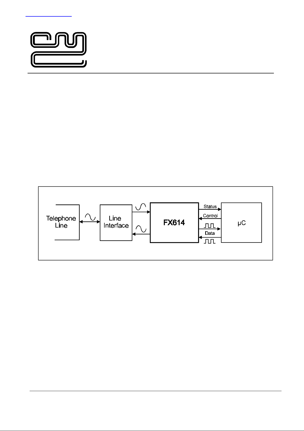
The FX614 is a low power CMOS integrated circuit for the reception or transmission of asynchronous
1200bits/sec data and is suitable for use in Bell 202 type systems. It is also capable of generating the
5bits/sec or 150bits/sec 'back channel'.
The device incorporates an optional Tx and Rx data retiming function that removes the need for a UART in the
associated
this is controlled by an external logic level.
The FX614 may be used in a wide range of telephone telemetry systems. With a low operating voltage of
3.0V, a very low current 'sleep' mode (1
terminal and line powered applications. A 3.58MHz standard Xtal/Clock rate is required and the device
operates from a 3.0V to 5.5V supply. Both SOIC (D4) and Plastic DIL (P3) 16-pin package types are available.
1997 Consumer Microcircuits Limited
µC when operating at 1200bits/sec. An optional line equaliser is incorporated into the receive path,
µA) and an operating current of 1mA the device is ideal for portable,

Bell 202 Compatible Modem FX614
CONTENTS
Section Page
1.0 Features ......................................................................................................1
1.1 Brief Description.........................................................................................1
1.2 Block Diagram ............................................................................................3
1.3 Signal List...................................................................................................3
1.4 External Components.................................................................................5
1.5 General Description....................................................................................5
1.5.1 Xtal Osc and Clock Dividers.......................................................5
1.5.2 Mode Control Logic ....................................................................6
1.5.3 Rx Input Amplifier.......................................................................6
1.5.4 Receive Filter and Equaliser.......................................................6
1.5.5 Energy Detector ..........................................................................7
1.5.6 FSK Demodulator ................................................................ ........7
1.5.7 FSK Modulator and Transmit Filter ................................ ............7
1.5.8 Rx Data Retiming ........................................................................9
1.5.9 Tx Data Retiming ................................................................ .......10
1.6 Application Notes.....................................................................................12
1.6.1 Line Interface.............................................................................12
1.7 Performance Specification.......................................................................13
1.7.1 Electrical Performance..............................................................13
1.7.2 Packaging..................................................................................16
1997 Consumer Microcircuits Limited 2 D/614/4
Bell 202 Compatible Modem FX614
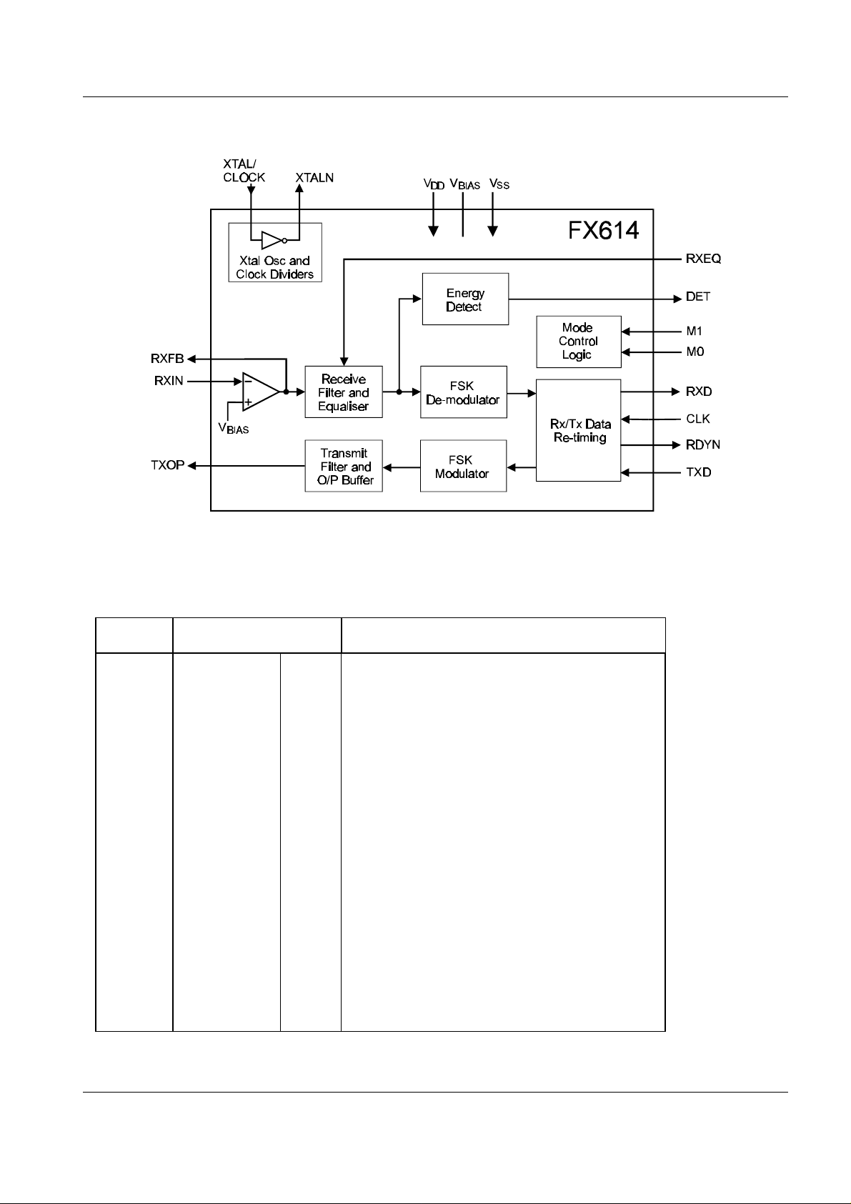
1.2 Block Diagram
1.3 Signal List
FX614
D4/P3
Pin No. Name Type
1 XTALN O/P The output of the on-chip Xtal oscillator inverter.
2 XTAL/CLOCK I/P The input to the on-chip Xtal oscillator inverter.
3 M0 I/P A logic level input for setting the mode of the
4 M1 I/P A logic level input for setting the mode of the
5 RXIN I/P Input to the Rx input amplifier.
6 RXFB O/P Output of the Rx input amplifier, and the input to
Signal Description
Figure 1 Block Diagram
device. See section 1.5.2.
device. See section 1.5.2.
the Rx filter.
7 TXOP O/P The output of the FSK generator.
8 V
1997 Consumer Microcircuits Limited 3 D/614/4
SS
Power The negative supply rail (ground).

Bell 202 Compatible Modem FX614
FX614
D4/P3
Signal Description
Pin No. Name Type
9 V
BIAS
O/P Internally generated bias voltage, held at VDD/2
when the device is not in 'Zero-Power' mode.
Should be decoupled to VSS by a capacitor
mounted close to the device pins.
10 RXEQ I/P A logic level input for enabling/disabling the
equaliser in the receive filter. See section 1.5.4.
11 TXD I/P A logic level input for either the raw input to the
FSK Modulator or data to be re-timed depending
on the state of the M0, M1 and CLK inputs. See
section 1.5.9.
12 CLK I/P A logic level input which may be used to clock
data bits in or out of the FSK Data Retiming
block.
13 RXD O/P A logic level output carrying either the raw
output of the FSK Demodulator or re-timed
characters depending on the state of the M0, M1
and CLK inputs. See section 1.5.8.
14 DET O/P A logic level output of the on-chip Energy Detect
circuit.
15 RDYN O/P "Ready for data transfer" output of the on-chip
data retiming circuit. This open-drain active low
output may be used as an Interrupt
Request/Wake-up input to the associated
µC.
An external pull-up resistor should be connected
between this output and VDD.
16 V
DD
Power The positive supply rail. Levels and thresholds
within the device are proportional to this voltage.
Should be decoupled to VSS by a capacitor
mounted close to the device pins.
Notes: I/P = Input
O/P = Output
This device is capable of detecting and decoding small amplitude signals. To achieve this V
DD
and V
BIAS
decoupling and protecting the receive path from extraneous in-band signals are very important. It is
recommended that the decoupling capacitors are placed so that connections between them and the device
pins are as short as practicable. A ground plane protecting the receive path will help attenuate interfering
signals.
1997 Consumer Microcircuits Limited 4 D/614/4
Bell 202 Compatible Modem FX614
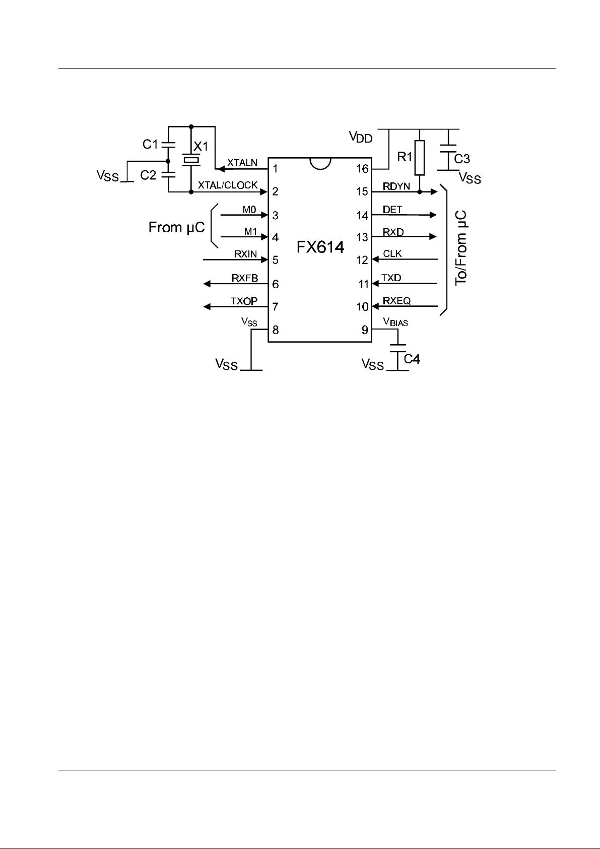
1.4 External Components
R1
100k
Ω
X1 3.579545MHz C3
Resistors
±5%, capacitors ±10% unless otherwise stated.
C1, C2 18pF
µF
0.1
C4
0.1
µF
Figure 2 Recommended External Components for Typical Application
1.5 General Description
1.5.1 Xtal Osc and Clock Dividers
Frequency and timing accuracy of the FX614 is determined by a 3.579545MHz clock present at the
XTAL/CLOCK pin. This may be generated by the on-chip oscillator inverter using the external components C1,
C2 and X1 of Figure 2, or may be supplied from an external source to the XTAL/CLOCK input. If supplied from
an external source, C1, C2 and X1 should not be fitted.
The on-chip oscillator is turned off in the 'Zero-Power' mode.
If the clock is provided by an external source which is not always running, then the 'Zero-Power' mode must be
set when the clock is not available. Failure to observe this rule may cause a significant rise in the supply
current drawn by FX614 as well as generating undefined states of the RXD, DET and RDYN outputs.
1997 Consumer Microcircuits Limited 5 D/614/4

Bell 202 Compatible Modem FX614
1.5.2 Mode Control Logic
The FX614's operating mode is determined by the logic levels applied to the M0 and M1 input pins:
M1 M0 Rx Mode Tx Mode
Data Retime
[1]
0 0 1200bits/sec 150bits/sec Rx
0 1 Off 1200bits/sec Tx
1 0 1200bits/sec Off / 5bits/sec Rx
1 1 'Zero-Power' -
[1] If enabled.
In the 'Zero-Power' (ZP) mode, power is removed from all internal circuitry. When leaving the 'ZP' mode there
must be a delay of 20ms before any Tx data is passed to, or Rx data read from, the device to allow the bias
level, filters and oscillator to stabilise. On applying power to the device the mode must be set to 'ZP', i.e. M0 =
'1', M1 = '1', until V
has stabilised.
DD
1.5.3 Rx Input Amplifier
This amplifier is used to adjust the received signal to the correct amplitude for the FSK receiver and Energy
Detect circuits (see section 1.6.1).
1.5.4 Receive Filter and Equaliser
Is used to attenuate out of band noise and interfering signals, especially the locally generated transmit tones
which might otherwise reach the 1200bits/sec FSK Demodulator and Energy Detector circuits. This block also
includes a switchable equaliser section. When the RXEQ pin is low, the overall group delay of the receive filter
is flat over the 1200bits/sec frequency range. If the RXEQ pin is high the receive filter's typical overall group
delay will be as shown in Figure 3.
Figure 3 Rx Equaliser Group Delay (RXEQ = '1') wrt 1700Hz
1997 Consumer Microcircuits Limited 6 D/614/4
 Loading...