


CMD CM1293-02SO, CM1293-02SO, CM1293-02SR, CM1293-02SR, CM1293-02ST Schematic [ru]
...
CM1293
2, 4, and 8-Channel Low Capacitance ESD Protection Arrays
Features
• 2, 4, and 8 channels of ESD protection
• Provides
ESD protection to IEC61000-4-2
- 8kV contact discharge
- 15kV air discharge
• Low loading capacitance of 2.0pF max.
• Low clamping voltage
• Channel I/O to I/O capacitance 1.5pF typical
• Zener diode protects supply rail and eliminates the
need for external by-pass capacitors
• Each I/O pin can withstand over 1000 ESD strikes
• Available in SOT, and MSOP packages
• Lead-free version available
Applications
• DVI ports, HDMI ports in notebooks, set top boxes,
digital TVs, LCD displays
• Serial ATA ports in desktop PCs and hard disk
drives
• PCI Express ports
• General purpose high-speed data line ESD
protection
Product Description
The CM1293 family of diode arrays has been designed
to provide ESD protection for electronic components or
sub-systems requiring minimal capacitive loading.
These devices are ideal for protecting systems with
high data and clock rates or for circuits requiring low
capacitive loading. Each ESD channel consists of a
pair of diodes in series which steer the positive or negative ESD current pulse to either the positive (V
negative (V
between V
protects the V
) supply rail. A Zener diode is embedded
N
and VN, offering two advantages. First, it
P
rail against ESD strikes, and second,
CC
it eliminates the need for a bypass capacitor that would
otherwise be needed for absorbing positive ESD
strikes to ground. The CM1293 will protect against
ESD pulses up to (±15kV air, ±8kV contact discharge)
per the IEC 61000-4-2 Level 4 standard.
This device is particularly well-suited for protecting systems using high-speed ports such as USB2.0,
IEEE1394 (Firewire
®, iLink™), Serial ATA, DVI, HDMI
and corresponding ports in removable storage, digital
camcorders, DVD-RW drives and other applications
where extremely low loading capacitance with ESD
protection are required in a small package footprint.
P
) or
The CM1293 family of devices is available with
optional lead-free finishing.
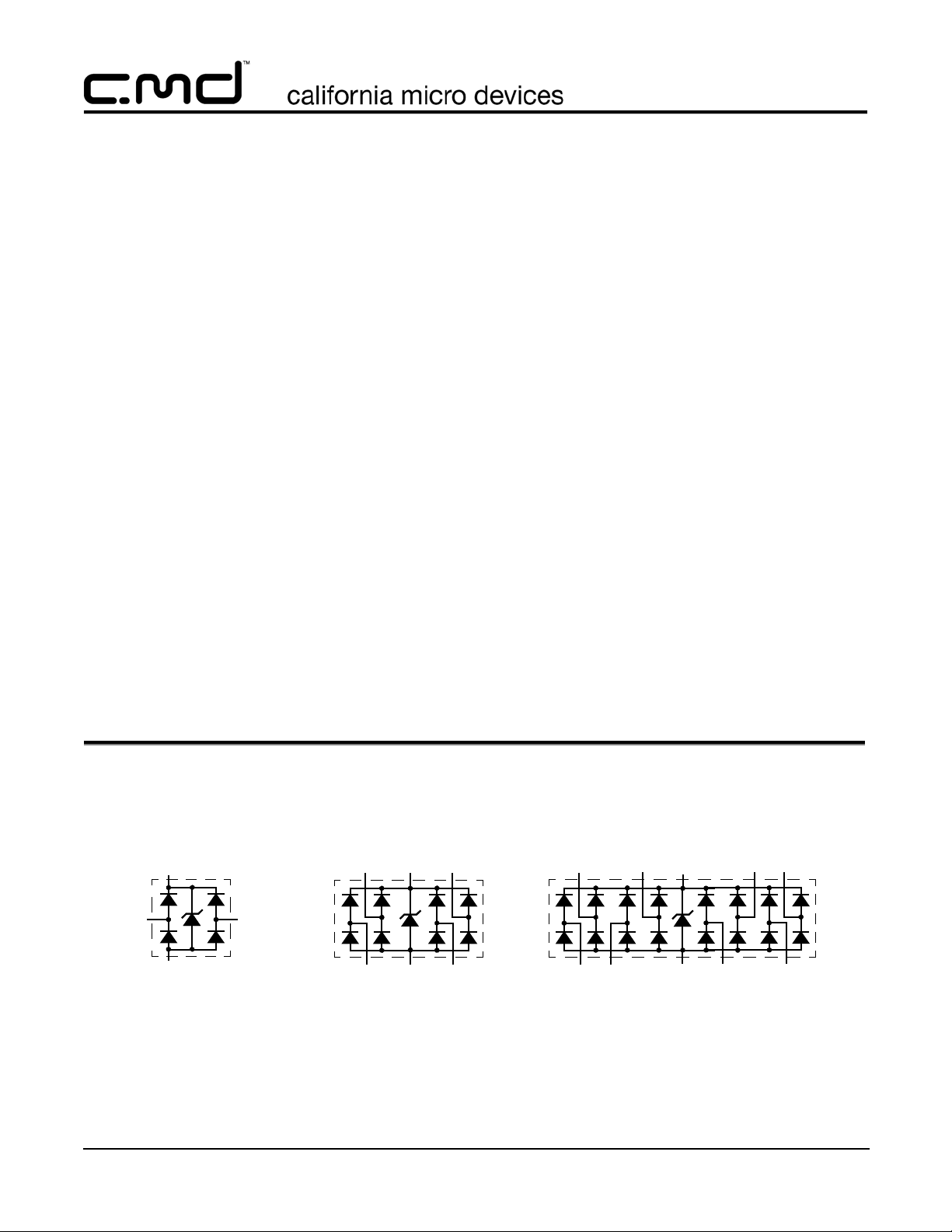
Electrical Schematics
CH6
V
P
CH1
V
N
CM1293-02ST/SO
CM1293--02SR
© 2006 California Micro Devices Corp. All rights reserved.
01/26/06 490 N. McCarthy Blvd., Milpitas, CA 95035-5112 ● Tel: 408.263.3214 ● Fax: 408.263.7846 ● www.cmd.com 1
CH2
CH4
CH1
CM1293-04ST/SO
CM1293-04MS/MR
CH3
V
P
CH2
V
N
CH8
CH1
CH7
CH2
CM1293-08MS/MR
V
P
CH3
V
N
CH5
CH4
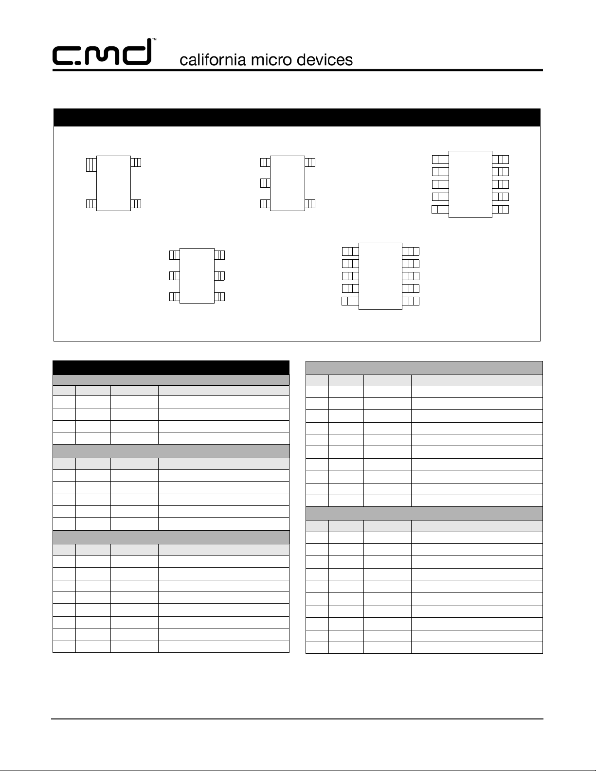
PACKAGE / PINOUT DIAGRAMS
CM1293
Top View
4
V
CH1
1
N
D036
2
V
P
3
CH2
4-Lead SOT143-4
Top View
CH1
CH2
1
D035
V
2
N
3
6-Lead SOT23-6
6
D034 /
5
4
Note: These drawings are not to scale.
PIN DESCRIPTIONS
2-CHANNEL, 4-LEAD SOT143-4 PACKAGE
PIN NAME TYPE PIN
V
1
2 CH1 I/O 2
3 CH2 I/O 3
4
PIN NAME TYPE DESCRIPTION
1 NC No connect
2V
3 CH1 I/O ESD Channel
4 CH2 I/O ESD Channel
5V
PIN NAME TYPE DESCRIPTION
1 CH1 I/O ESD Channel
2V
3 CH2 I/O ESD Channel
4 CH3 I/O ESD Channel
5V
6 CH4 I/O ESD Channel
5V
6 CH4 I/O ESD Channel
N
V
P
N
P
N
P
P
GND 1
PWR
2-CHANNEL, 5-LEAD SOT23-5 PACKAGE
GND Negative voltage supply rail
PWR Positive voltage supply rail
4-CHANNEL, 6-LEAD SOT23-6 PACKAGE
GND Negative voltage supply rail
PWR Positive voltage supply rail
PWR Positive voltage supply rail
Top View
1
NC
2
V
N
CH1
3
5-Lead SOT23-5
D032 /
D033
5
V
P
4
CH2
CH1
CH2
CH3
CH4
V
Top View
1
2
3
4
N
56
10-Lead MSOP-10
D039
10
D038 /
CH8
9
CH7
V
8
7
P
CH6
CH5
Top View
1
CH4
V
P
CH3
CH1
NC
V
CH2
P
10
2
D040 /
D041
3
4
56NC CH3
10-Lead MSOP-10
4-CHANNEL, 10-LEAD MSOP-10 PACKAGE
PIN NAME TYPE DESCRIPTION
1 CH1 I/O ESD Channel
2 NC No connect
3V
4 CH2 I/O ESD Channel
4
5 NC No connect
6 CH3 I/O ESD Channel
7 NC No connect
8V
9 CH4 I/O ESD Channel
10 NC No connect
PIN NAME TYPE DESCRIPTION
1 CH1 I/O ESD Channel
2 CH2 I/O ESD Channel
3 CH3 I/O ESD Channel
4 CH4 I/O ESD Channel
5V
6 CH5 I/O ESD Channel
7 CH6 I/O ESD Channel
8V
9 CH7 I/O ESD Channel
10 CH8 I/O ESD Channel
P
N
N
N
PWR Positive voltage supply rail
GND Negative voltage supply rail
8-CHANNEL, 10-LEAD MSOP-10 PACKAGE
PWR Positive voltage supply rail
GND Negative voltage supply rail
NC
CH4
9
V
8
7
N
NC
© 2006 California Micro Devices Corp. All rights reserved.
2 490 N. McCarthy Blvd., Milpitas, CA 95035-5112 ● Tel: 408.263.3214 ● Fax: 408.263.7846 ● www.cmd.com 01/26/06
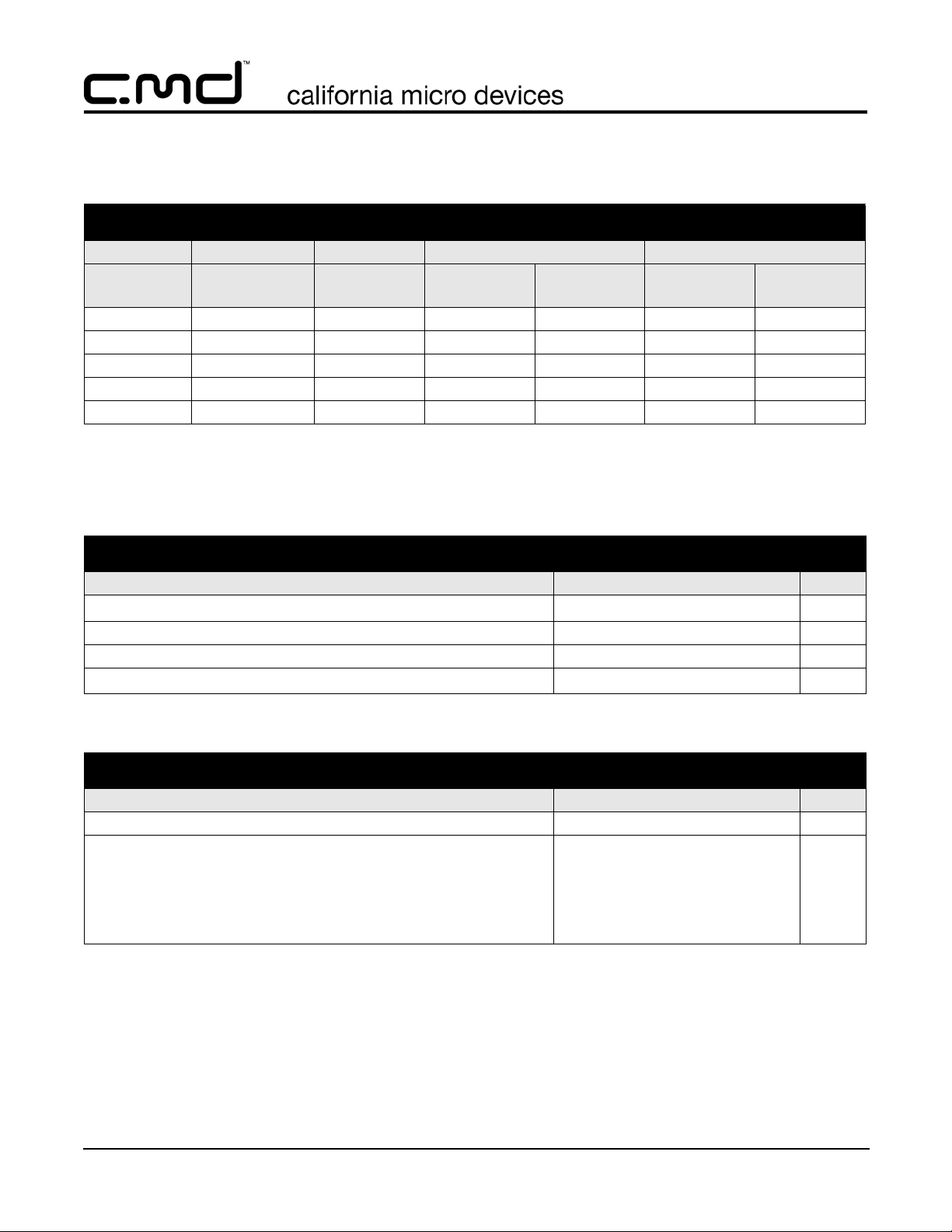
Ordering Information
PART NUMBERING INFORMATION
# of Channels Leads Package
2 4 SOT143-4 CM1293-02SR D036
2 5 SOT23-5 CM1293-02ST D032 CM1293-02SO D033
4 6 SOT23-6 CM1293-04ST D034 CM1293-04SO D035
4 10 MSOP-10 CM1293-04MS D040 CM1293-04MR D041
8 10 MSOP-10 CM1293-08MS D038 CM1293-08MR D039
Note 1: Parts are shipped in Tape & Reel form unless otherwise specified.
Specifications
Standard Finish Lead-free Finish
Ordering Part
Number
1
Part Marking
Ordering Part
Number
1
CM1293
Part Marking
ABSOLUTE MAXIMUM RATINGS
PARAMETER RATING UNITS
Operating Supply Voltage (V
Operating Temperature Range -40 to +85 °C
Storage Temperature Range -65 to +150 °C
DC Voltage at any channel input (V
- VN)6.0V
P
- 0.5) to (VP + 0.5) V
N
STANDARD OPERATING CONDITIONS
PARAMETER RATING UNITS
Operating Temperature Range -40 to +85 °C
Package Power Rating
SOT143-4 Package (CM1293-02SR)
SOT23-5 Package (CM1293-02ST/SO)
SOT23-6 Package (CM1293-04ST/SO)
MSOP-10 Package (CM1293-04MS/MR)
MSOP-10 Package (CM1293-08MS/MR)
225
225
225
400
400
mW
mW
mW
mW
mW
© 2006 California Micro Devices Corp. All rights reserved.
01/26/06 490 N. McCarthy Blvd., Milpitas, CA 95035-5112 ● Tel: 408.263.3214 ● Fax: 408.263.7846 ● www.cmd.com 3
Specifications (cont’d)
CM1293
ELECTRICAL OPERATING CHARACTERISTICS
1
SYMBOL PARAMETER CONDITIONS MIN TYP MAX UNITS
V
I
V
I
LEAK
C
Operating Supply Voltage (VP-VN)3.35.5V
P
Operating Supply Current (VP-VN)=3.3V 8.0 μA
P
Diode Forward Voltage
F
Top Diode
Bottom Diode
IF = 8mA; TA=25°C
0.60
0.60
0.80
0.80
0.95
0.95
V
V
Channel Leakage Current TA=25°C; VP=5V, VN=0V ±0.1 ±1.0 μA
Channel Input Capacitance At 1 MHz, VP=3.3V, VN=0V, VIN=1.65V;
IN
2.0 pF
Note 2
ΔC
V
ESD
Channel I/O to I/O capacitance 1.5 pF
IO
ESD Protection
Peak Discharge Voltage at any
channel input, in system
a) Contact discharge per
Notes 2, 4 & 5; T
=25°C
A
±8
kV
IEC 61000-4-2 standard
b) Human Body Model,
MIL-STD-883, Method
Notes 2, 3 & 5; T
=25°C
A
±15
kV
3015
R
V
DYN
Channel Clamp Voltage
CL
Positive Transients
Negative Transients
Dynamic Resistance
Positive Transients
Negative Transients
At 8kV ESD HBM; TA=25°C; Notes 2 & 3
TA=25°C; Notes 5 & 6
+9.0
-9.0
1.2
0.6
V
V
Ω
Ω
Note 1: All parameters specified at TA = -40°C to +85°C unless otherwise noted.
Note 2: These parameters guaranteed by design and characterization.
Note 3: Human Body Model per MIL-STD-883, Method 3015, C
Note 4: Standard IEC 61000-4-2 with C
Note 5: These measurements performed with no external capacitor on V
Note 6: Measured under pulsed conditions, pulse width = 0.7mS, maximum current = 1.5A.
© 2006 California Micro Devices Corp. All rights reserved.
Discharge
= 150pF, R
Discharge
= 100pF, R
Discharge
= 330Ω, VP = 3.3V, VN grounded.
.
P
Discharge
= 1.5KΩ, VP = 3.3V, VN grounded.
4 490 N. McCarthy Blvd., Milpitas, CA 95035-5112 ● Tel: 408.263.3214 ● Fax: 408.263.7846 ● www.cmd.com 01/26/06